國
立
交
通
大
學
電信工程研究所
博
士
論
文
多頻濾波器耦合矩陣之合成及其
實現於微帶線平行耦合濾波器結構之研究
Synthesis of Multi-band Coupling Matrix and Its Implementation of
Microstrip Parallel-coupled Filter Structures
研 究 生:郭益廷 (Yi-Ting Kuo)
指導教授:張志揚 教授 (Chi-Yang Chang)
多頻濾波器耦合矩陣之合成及其實現於微帶線平行耦合濾波器
結構之研究
Synthesis of Multi-band Coupling Matrix and Its Implementation of
Microstrip Parallel Coupled Filter Structures
研 究 生:郭益廷 Student:Yi-Ting Kuo
指導教授:張志揚 Advisor:Chi-Yang Chang
國 立 交 通 大 學
電信工程研究所
博 士 論 文
A Dissertation Submitted toDepartment of Communication Engineering
College of Electrical Engineering and Computer Engineering National Chiao Tung University
In partial Fulfillment of the Requirements For the Degree of Doctor of Philosophy
in
Communication Engineering October 2011
Hsinchu, Taiwan, Republic of China
i
多頻濾波器耦合矩陣之合成及其實現於微帶線平行耦合濾波
器結構之研究
研究生: 郭益廷 指導教授: 張志揚 博士
國立交通大學電信工程研究所
摘
要
本論文研究主題為一個完整設計雙頻與多頻濾波器的流程,並實現於微帶線 平行耦合濾波器架構上。首先提出一種新的全解析式的多頻濾波器耦合矩陣合成 技術,透過簡單的操作,將廣為人知的單頻濾波器耦合矩陣合成技術推廣至多頻 應用。此提出的技術可以保證其產生之響應遵守廣義柴比雪夫特性,亦即在多頻 濾波器各通帶保持等漣波特性。接著,將此合成技術所生成之耦合矩陣轉換到可 實現的耦合架構上。本文提出單路徑式與雙路徑式耦合架構,並且對於其在雙頻 濾波器應用上進行比較與分析。透過對應其耦合矩陣之耦合係數與平行耦合濾波 器的設計參數,可以分別設計出每個路徑所對應的平行耦合濾波器。對於雙路徑 式架構,需要兩個同向雙工器將兩路徑連接以完成雙頻濾波器設計。接著,為了 進一步縮小雙頻濾波器的面積,本文使用山型雙模諧振腔的雙模特性來設計縮小 化的雙頻濾波器。透過山型諧振腔的奇、偶模分析可以找出其適當的濾波器耦合 架構即為雙路徑式耦合架構,並且可以透過分析將耦合矩陣對應至濾波器設計參 數上。此對應方法為一全解析式的流程,可以提供設計者有效率的雙模雙頻濾波 器設計。同樣的,在三頻與四頻濾波器設計中,三路徑式與四路徑式的架構可以 用來設計其所需要的耦合矩陣。接著透過將兩相鄰頻帶當作一個群組,變成雙頻 濾波器加單頻濾波器(針對三頻濾波器)或者雙頻濾波器加雙頻濾波器(針對四頻濾 波器)的群組。其中雙頻濾波器或單頻濾波器均可由其耦合矩陣對應之耦合係數和 山形諧振腔的設計參數進行合成。最後再將所產生的兩個濾波器透過兩個同向雙 工器相接,形成所需要的三頻或四頻濾波器。
ii
Synthesis of Multi-band Coupling Matrix and Its Implementation of
Microstrip Parallel-coupled Filter Structures
Student: Yi-Ting Kuo Advisor: Dr. Chi-Yang Chang
Institute of Communication Engineering
National Chiao Tung University
Abstract
The research topic in this dissertation is a complete design flow for dual-band and multi-band filter synthesis, and these synthesized filters are implemented using microstrip parallel-coupled lines structures. First of all, a novel fully analytical multi-band coupling matrix synthesis technique is provided. By simple operations, the well-known single-band coupling matrix synthesis technique is then extended for the multi-band filter design. The proposed technique guarantees the original single-band equal-ripple property within each passbands following each single-band generalized Chebyshev characteristic. Furthermore, the requested coupling matrix should be transferred into the realistic coupling schemes for the practical implementation. In this dissertation, single-path and dual-path coupling schemes are provided, and the properties of each coupling scheme will be discussed. Moreover, the design parameters of the parallel-coupled filter are related with the components of the coupling matrix, the practical parallel-coupled filter for each path will be synthesized. For the dual-path topology, the synthesized dual-band filter needs double-diplexing configuration to connect two filters of two paths. In order to further reduce the size of dual-band filters, the E-shaped resonator is proposed for its two-mode property and is useful for the
iii
development of miniaturized dual-band filters. By even- and odd-mode analysis of the E-shaped resonator, the dual-path coupling scheme is chosen for the dual-band filter design, and the practical design parameters of the dual-band filter will be extracted based on the corresponding coupling matrix. And such synthesis procedure is fully analytical and it provides an efficient design flow for the designer. Similarly, for the tri-band and quad-band filter design, the tri-path and quad-path coupling schemes are used for the coupling matrix synthesis. After grouping two adjacent passbands, the tri-band response will be separated into one dual-band response and one single-band response; and the quad-band response will be separated into two dual-band responses. In each grouped dual-band and single-band response, the corresponding E-shaped filter can be synthesized based on the corresponding coupling matrices. Finally, the double-diplexing configuration is used to connect two filters and then the tri-band or quad-band filter synthesis will be completed.
iv
誌謝
首先我要感謝我的指導教授張志揚博士,若不是張教授願意收留我並且給予 我很多學術上的協助與生活上的言教與身教,這個學位我不會有機會拿到。此外, 我要特別感謝來參與我口試並且給我意見使本論文更加完美的口試委員,分別是 郭仁財教授、鍾世忠教授、黃瑞彬教授、紀佩綾教授、王暉教授、邱煥凱教授、 林祐生教授、湯敬文教授。謝謝老師們給與寶貴的意見、指教以及鼓勵。在這裡 再一次的表達我對老師們的感謝。 對於博士生來說,博士學位象徵著是一種研究方法學習的認可,而更多的, 是一種對於學術、對於人與人之間的關係和對於未來人生規劃上的一種磨練與學 習。在這一路上,有很多的不確定感和挫折,從想放棄到最後終於到達目的地, 實在是有太多的人需要感謝了。首先我要感謝趙學永博士,趙博士是我在交通大 學的第一任指導教授,從我碩一開始,不斷的鼓勵我也教導我很多做學問的堅持 以及方向。趙博士從不嫌煩的總是對我有問必答,也刺激我在思考學術問題上面 有更嚴謹的態度。此外,若是說我後來做研究有足夠的程式背景做為開發工具, 一定是來自於趙博士對我在程式上的訓練以及教誨。然而趙博士在我求學過程中 往國外業界發展,而我當時不夠成熟,所以婉拒了趙博士繼續指導的美意。若說 我在博士生涯有何遺憾,此必定為最。 再經歷過另一位教授的指導,但因在學術理念上的不合以及心態上的不適應, 我選擇中途休息。感謝電信所的陳伯寧教授以及鍾世忠教授在擔任電信所所長期 間對於我的更換指導教授的事情上面多所幫忙,也感謝趙學永博士不計前嫌的書 信往返的協助,讓我能順利的更換到張志揚教授的研究群。而我更要感謝張志揚 教授的提攜與其在學術上的引導,張教授開朗而自由的風格以及在研究上的正直 與堅持,讓我重新對於人生有不同的體悟以及看法。張教授的言行合一的態度以 及他對生活的喜愛和對學術的熱誠,讓我受益良多,而能在這樣充滿愛以及信任 的研究室裡做研究,也才真的能夠有時間思考新的創意以及有新的想法。v 而在我休學前的低潮與沮喪的時期,感謝諮商中心的許瑛玿老師的協助與傾 聽,給我很多建議以及鼓勵,讓我的博士生涯能走到最後開花結果。也感謝瑛玿 老師為了學生的權益能夠為學生抵擋來自師長方面的壓力。也謝謝瑛玿老師最後 建議我參與志工服務。那是我在博士生涯當中最重要的一個轉折點。而休學期間, 感謝由朱永祥主任所組織的伊甸基金會的服務遊學團,能夠透過到偏遠地區服務, 來重新思考自己的定位以及人生的看法。也要謝謝張志揚教授對於我不時參加志 工活動的包容以及肯定。 而在博士生涯中,最重要也最親近的,莫過於實驗室的朝夕相處的夥伴。我 要謝謝 718 實驗室的至鴻、逸宏、阿郎、小宇、震軒、譽闡學長、旻靜學姐,以 及夥伴哲宇、培育、義志和學弟翔昱、當榮和學妹佳伶、慧玲、小雪,有你們總 是讓 718 生氣滿滿,也度過不少熬夜寫程式的漫漫長夜。謝謝電資六樓的紹銘學 長與典燁、大慶、宣銘學弟,度過了最難熬的日子,也能苦中作樂每天有笑有鬧 有志一同。特別要感謝至鴻與譽闡,在人生的道路上給予很多建議以及鼓勵。還 有佳伶與慧玲,謝謝妳們總是在做很多人生大事的時候記得拉我一起去,人生第 一次環島真得是很開心。謝謝 916 實驗室的竟谷學長,對於一個未曾蒙面的學弟 能夠傾囊相授,讓我很快的在微波濾波器研究上能很快上軌道,也謝謝你提供我 在學校最後的時光可以有機會去業界打工增廣見聞。謝謝哲慶,在我更換指導教 授事上有很多幫忙以及建議,也在我濾波器的研究上給予很多建議與方法。感謝 金雄學長,讓我在實驗室的生活有歸屬感,也有很多的討論與協助。感謝建育學 長總是帶給實驗室很多歡樂的笑話以及三不五時的關心,讓實驗室總是有很溫馨 的氣氛。此外,感謝一起朝博士路邁進的正憲給與我很多生活上與學術上的協助, 還有一起爬山一起騎車體驗大自然的美,是我在 916 很美好的回憶。坐在隔壁位 置昀緯是最常能一起討論一起研究一起出國報論文真的是有革命情感。感謝維欣 也一起陪騎了北橫和司馬庫斯,騎腳踏車可以成行真的是很開心。感謝忠傑、如 屏、殿靖、耿宏,實驗室可以常常一起唱歌吃飯真得是很歡樂也很窩心。唱歌電 影咖佩傑也是實驗室解憂與作業寫不出來解憂的必備人選。世峰、揚達、聖智、
vi 鵬達、義傑、梓淳還有老是被我欺負的學妹們宛蓉、懿萱、士鈺和祥蓉,有你們 在真的是讓實驗室生色不少。尤其是宛蓉,真是辛苦妳在我的帶領下做了很多辛 苦事和腦包事。至於新進來的大學姐弘偉、皓宇、若宜、郁叡,實驗室的美好正 等著妳們探索。 這裡也要特別感謝Camy, 最後這一段時間謝謝妳不時的鼓勵與分享,讓我能 專心也安心的在研究上面努力。 最後,我最要感謝得是我的家人,我也想將這篇論文獻給,我的父親郭榮樹、 我的母親翁毓嬪,謝謝你們的辛苦栽培,讓我在博士的生涯上無後顧之憂,也謝 謝哥哥郭奕良、郭奕成,能成全我到三十歲還能繼續求學。我也要趁這個機會感 謝從小照顧我長大的奶奶郭黃水河、爺爺郭蟬,以及在小學到大學時期不時關心 我生活的外公翁耀清,外婆翁楊罔市,沒有你們的愛與關懷,不會有現在的我。 郭益廷 於新竹交大 2011 年 11 月 14 號
vii
Contents
Abstract (Chinese) ... i
Abstract ... ii
Acknowledgement ... iv
Contents ... vii
List of Tables ... ix
List of Figures ... xi
Chapter 1 Introduction ... 1
1.1 Research Motivation ... 1
1.2 Literature Survey ... 3
1.3 Contribution ... 8
1.4 Organization ... 9
Chapter 2 Fully-Analytical Multi-band Coupling Matrix Synthesis ... 11
2.1 Introduction ... 11
2.2 Analytical Multi-band Filtering Function Synthesis ... 11
2.3 Frequency Transformation ... 19
2.4 Computational Examples ... 21
2.4.1 Example 1: Symmetric Dual-band Bandpass Filter ... 21
2.4.2 Example 2: Asymmetric Dual-band Bandpass Filters ... 26
2.4.3 Example 3: Multiband Bandpass Filters ... 33
2.5 Comparison with Other Method ... 37
2.6 Other Properties in the Proposed Method ... 39
2.6.1 Passbands with Different Return Loss ... 40
2.6.2 Closely Adjacent Passbands ... 42
2.6.3 Intrinsic Transmission Zero ... 45
2.7 Conclusion ... 47
Chapter 3 Dual-band Filter Design Using Parallel-Coupled Line ... 48
3.1 Introduction ... 48
3.2 Single-path Coupling Scheme ... 49
3.3 Dual-path Coupling Scheme ... 51
3.4 Transmission Zeros Determination in Single-path and Dual-path Coupling Schemes ... 55
3.4.1 Single-path Dual-band Filter Characteristic ... 56
3.4.2 Symmetric Dual-path Dual-band Filter Characteristic ... 58
3.4.2 Asymmetric Dual-path Dual-band Characteristic ... 61
3.5 Analytical Approach for Dual-band Filter Design Using Parallel-Coupled Lines ... 64
viii
3.6 Microstrip Implementation for Single-path and Dual-path Dual-band filters ... 69
3.6.1 The Single-path Dual-band Filter ... 70
3.6.2 The Symmetric Dual-path Dual-band Filter ... 72
3.6.3 The Asymmetric Dual-path Dual-band Filter ... 74
3.7 Conclusion ... 77
Chapter 4 Two-mode Dual-band Filter Design Using E-shaped Resonators ... 79
4.1 Introduction ... 79
4.2 E-shaped Resonator ... 80
4.3 Analytical Approach in Two-mode Dual-band Filter Design Using E-shaped Resonators ... 81
4.3.1 Analytical Approach for the Odd-mode Analysis ... 83
4.3.2 Analytical Approach for the Even-mode Analysis ... 83
4.3.3 Impact of the Constrained Even-Mode ke on the Filter Performance ... 90
4.3.4 Analytical Calculation Example: Fourth-order Two-mode Dual-band Bandpass Filter ... 94
4.4 Examples for Practical Filter Implementation ... 99
4.4.1 Example 1: Fourth-order Two-mode Dual-band Bandpass Filter with 4 Transmission Zeros ... 99
4.4.2 Example 2: Sixth-order Two-mode Dual-band Bandpass Filter ... 105
4.5 Conclusion ... 110
Chapter 5 Two-mode Tri-band and Quad-band Filter Design with Close Adjacent Passbands Using E-shaped Resonators ... 112
5.1 Introduction ... 112
5.2 Double Diplexing Configuration ... 113
5.3 Tri-band and Quad-band Filter Synthesis ... 114
5.3.1 Example 1: Tri-band Filter ... 114
5.3.2 Example 2: Quad-band Filter ... 119
5.4 Conclusion ... 123
Chapter 6 Conclusion and Future Work ... 124
6.1 Conclusion ... 124
6.2 Future Work ... 125
ix
List of Tables
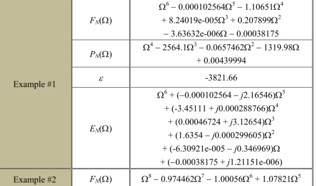
Table 2.1 The Requested Frequency Variables in Example 1. ... 22
Table 2.2 The Requested Setting Variables in Synthesis Procedure in Example 1... 23
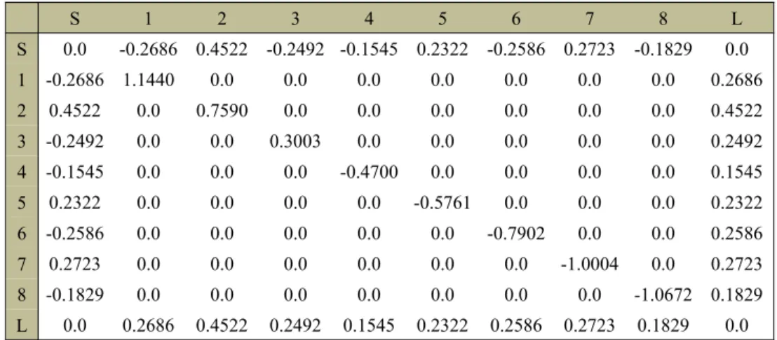
Table 2.3 Transversal Coupling Matrix for the Example 1. ... 24
Table 2.4 The Polynomials in (2-8) in the Example 1... 24
Table 2.5 Roots of Non-passive and Passive EN(Ω). ... 25
Table 2.6 The Requested Frequency Variables in Example 2. ... 27
Table 2.7 The Requested Setting Variables in Synthesis Procedure in Example 2... 28
Table 2.8 The Polynomials in (2-8) in the Example 2... 28
Table 2.9 Transversal Coupling Matrix for the Example 2 without Transmission Zeros Adjustment. ... 30
Table 2.10 Transversal Coupling Matrix for the Example 2 with Transmission Zeros Adjustment. ... 32
Table 2.11 The Polynomials in (2-8) in the Example 3... 34
Table 2.12 Transversal Coupling Matrix for the Example 3 ... 37
Table 2.13 The Specifications for the Method Comparison ... 38
Table 2.14 The Transversal Coupling Matrix for the dual-band filter in Figure 2-13 ... 40
Table 2.15 The Polynomials for the Dual-band Filter in Figure 2-13. ... 41
Table 2.16 The Synthesized Polynomials in Two Examples with Closely Adjacent Passbands ... 43
Table 3.1 The Transversal Coupling Matrix for the Dual-band Filter in Figure 3-1. .... 50
Table 3.2 The Coupling Matrix for the Dual-band Filter in Figure 3-1 with Coupling Scheme in Figure 3-2. ... 51
Table 3.3 The Transversal Coupling Matrix for the Dual-band Filter in Figure 3-3 ... 53
Table 3.4 (a) The Transversal Coupling Matrix for the Upper Path (M1). (b) The Transversal Coupling Matrix for the Lower Path (M2). ... 53
Table 3.5 Rotation Sequence for Reduction of the Transversal Matrix to the Requested Matrix with Topology in Figure 3-4 ... 54
Table 3.6 The Coupling Matrix for the Dual-band Filter in Figure 3-3 with the Dual-path Coupling Scheme shown in Figure 3-4. ... 54
Table 3.7 The Coupling Matrix of the Single-path Dual-band Filter ... 56
Table 3.8 The Coupling Matrix of the Symmetric Dual-path Dual-band Filter ... 59
Table 3.9 The Coupling Matrix of the Asymmetric Dual-band Filter. ... 62
Table 3.10 The Coupling Matrix of the Dual-band Filter for GPS System Design. ... 65
Table 3.11 The Calculated Parameters for the Parallel-Coupled Line of the Upper Path. ... 66 Table 3.12 The Calculated Parameters for the Parallel-Coupled Line of the Lower Path.
x
... 67
Table 3.13 The Tuned Lengths of the Parallel-Coupled Line in Figure 3-12 and Figure 3-13 ... 67
Table 3.14 The Final Lengths of the Dual-band Filter for GPS System. ... 69
Table 3.15 Dimensions for the Layout Shown in Figure 3-17. (Unit: mm) ... 71
Table 3.16 Dimensions for the Layout Shown in Figure 3-20. (Unit: mm) ... 73
Table 3.17 Dimensions for the Layout Shown in Figure 3-23. (Unit: mm) ... 75
Table 4.1 Coupling Matrix for the Two-mode Dual-band Filter ... 95
Table 4.2 The Calculated Impedances for the Odd-mode Analysis ... 96
Table 4.3 The Coupling Matrix for the Filter in Example 1... 101
Table 4.4 The Calculated Impedances for the Odd-mode Analysis in Example 1. ... 101
Table 4.5 The Dimensions in Figure 4-23 (Unit: mm) ... 103
Table 4.6 The Coupling Matrix for Dual-band Filter in Example 2... 106
Table 4.7 The Calculated Impedances for the Odd-mode Analysis in Example 2. ... 108
Table 4.8 The Dimensions in Figure 4-31 (Unit: mm) ... 109
Table 5.1 Setting of Tri-band Coupling Matrix Synthesis ... 115
Table 5.2 Coupling Matrix of the Tri-band Filter ... 115
Table 5.3 Synthesized Zoe and Zoo Based on Coupling Matrix in Table 5.2 ... 116
Table 5.4 Synthesized Electrical Lengths and Stub Impedances Based on Coupling Matrix in Table 5.2 ... 117
Table 5.5 Dimensions of the Tri-band Filter (Unit: mm) ... 118
Table 5.6 Setting of Quad-band Coupling Matrix Synthesis... 119
Table 5.7 Coupling Matrix of the Quad-band Filter in Example 2. ... 119
Table 5.8 Synthesized Zoe and Zoo Based on Coupling Matrix in Table 5.7. ... 121
Table 5.9 Synthesized Electrical Lengths and Stub Impedances Based on Coupling Matrix in Table 5.7 ... 121
xi
List of Figures
Figure 2-1. The procedure of the single-band coupling matrix synthesis [90]... 13 Figure 2-2. The response of the 3rd order filtering function. (a) The linear scale. (b) The log scale. ... 14 Figure 2-3. The performance of the 4th order dual-band filtering function. ... 15 Figure 2-4. The passivity enforcement for polynomial EN(Ω). ... 18
Figure 2-5. The requested design variables in the bandpass domain and the lowpass domain. RL is the prescribed return loss. ... 20 Figure 2-6. (a) Filtering functions for two single-band filters of same order 3 (CN1 has
the transmission zeros at -1.5 and central frequency -0.75 rad/s and CN2 has
the transmission zeros at 1.5 and central frequency 0.75 rad/s), and the composite dual-band filtering function (CN1 // CN2). The in-band return loss
level is 20 dB in each case. (b) Corresponding S11 and S21 for the symmetric
dual-band filter in lowpass and bandpass domains... 26 Figure 2-7. (a) Filtering functions for two single-band filters of different order 3 (CN1
has the transmission zeros at -1.433 rad/s and 0.004 rad/s and central frequency -0.696 rad/s, and its multi-band lowpass domain bandwidth δ1 is
0.607 rad/s.) and order 5 (CN2 has the transmission zeros at 0.004 rad/s and
1.482 rad/s and central frequency 0.756 rad/s, and its multi-band lowpass domain bandwidth δ2 is 0.486 rad/s), and the composite dual-band filtering
function (CN1 // CN2). The in-band return loss level is 20 dB in each case. (b)
Corresponding S11 and S21 for the symmetric dual-band filter in lowpass
domains. ... 27 Figure 2-8. (a) Two third-order filtering functions. Solid line: filtering function has two finite transmission zeros at -6 and 0 rad/s, and the central frequency is -3 rad/s on the normalized lowpass domain. Dashed line: filtering function with 3 finite transmission zeros at -6, 0 and 6 rad/s, and the central frequency is -3 rad/s on the original lowpass domain. The in-band return loss is 20 dB in each case. (b) The corresponding S11 and S21. ... 31
Figure 2-9 Filtering functions for two single-band filters of different order 3 (CN1 has
the transmission zeros at -1.433, 0.0037, and 1.4134 rad/s and central frequency -0.696 rad/s and its milti-band lowpass domain bandwidth δ1 is
0.6066 rad/s.) and order 5 (CN2 has the transmission zeros at 0.0037 rad/s
and 1.4818 rad/s and central frequency 0.7566 rad/s with its multi-band lowpass domain bandwidth δ2 is 0.4857 rad/s), and the composite dual-band
filtering function (CN1 // CN2). The in-band return loss is 20 dB in each case.
xii
domains. ... 32 Figure 2-10 The S-parameters for the synthesized dual-band filter in Example 2. ... 33 Figure 2-11 (a) Filtering functions for four single-band filters of degree 3 (CN1 has
transmissions zeros at -1.2 and -0.6 rad/s and the central frequency at -0.9 rad/s), degree 4 (CN2 has transmissions zeros at -1.3, -0.65, and 0.01 rad/s
and the central frequency at -0.3 rad/s), degree 5 (CN3 has transmissions
zeros at -1.3, -0.6, -0.01, 0.63 and 1.3 rad/s and the central frequency at 0.3 rad/s), and degree 3 (CN4 has transmissions zeros at 1.35 and 0.9 rad/s and
the central frequency at 0.6 rad/s), and the composite quad-band filter (CN1 //
CN2 // CN3 // CN4 ). The in-band return loss is 20 dB in each case. (b) The
corresponding S11 and S21 for the quad-band filter. ... 34
Figure 2-12 Frequency responses of the dual-band filter composed of the third- and fifth-order filtering functions. Solid line: the proposed method. Dashed line: the analytical iterative method. ... 38 Figure 2-13 Filtering functions for two single-band filters of order 3 with return loss 20 dB (CN1 has the transmission zeros at -1.5714 and 2.1429 rad/s and the
central frequency -0.7143 rad/s with the multi-band lowpass domain bandwidth δ1 of 0.5724 rad/s) and order 5 with return loss 40 dB (CN2 has
the transmission zero at 2.1429 rad/s the and the central frequency 0.7143 rad/s with the multi-band lowpass domain bandwidth δ2 of 0.5718 rad/s),
and the composite dual-band filtering function (CN1 // CN2). (b)
Corresponding S11 and S21 for the symmetric dual-band filter in lowpass
domains. ... 41 Figure 2-14 The S-parameters for the filters with two close adjacent passbands with
polynomials in Table 2.16. (a) Equal ripple level, and (b) different ripple level. ... 44 Figure 2-15 (a) Two odd-order filtering functions have been combined as a dual-mode
filtering function with an extra transmission zeros, while two even-order filtering functions have been combined as a dual-mode filtering function has worse isolation between two passbands. ... 45 Figure 2-16 Two passbands with different order. (a) The odd-order upper passband and even-order lower passband are combined as the filtering function has an intrinsic transmission zero. (b) The even-order upper passband and odd-order lower passband are combined as the filtering function has no intrinsic transmission zero using the proposed method. But with Ω = −Ω operation in the settings of (a), the extra intrinsic transmission zero can be introduced. ... 46
xiii
Figure 3-1 (a) Filtering functions for two single-band filters of degree 2 (CN1 has the
transmission zero at 0 rad/s and the central frequency at -0.75 ras/s, and CN2
has the transmission zero at 0 rad/s and the central frequency at 0.75 rad/s), and the composite dual-band filter (CN1 // CN2). The in-band return loss level
is -20 dB in each case. (b) The corresponding S11 and S21 for the dual-band
filter. ... 50 Figure 3-2 The single-path coupling scheme for the dual-band filter in Figure 3-1. ... 51 Figure 3-3 (a) Filtering functions for two single-band filters of degree 3 (CN1 has the
transmission zero at -1.8 rad/s and the central frequency at -0.8 rad/s, and CN2 has the transmission zero at 1.8 rad/s and the central frequency at 0.8
rad/s), and the composite filter (CN1 // CN2). The in-band return loss level is
-20 dB in each case. (b) The corresponding S11 and S21 for the dual-band
filter. ... 52 Figure 3-4 The dual-path coupling scheme for the dual-band filter in Figure 3-3. ... 53 Figure 3-5 The performance of the single-path dual-band filter and the corresponding
dual-path coupling scheme based on the coupling matrix in Table 3.7. ... 57 Figure 3-6 The performances for the single-path dual-band filter without cross coupling (a) path S-3 and (b) path 6-L. ... 58 Figure 3-7 The performance of the symmetric dual-band filter and the corresponding
dual-path coupling scheme based on the coupling matrix in Table 3.8. ... 61 Figure 3-8 The performances of the (a) upper path and (b) lower path in the symmetric dual-band filter... 61 Figure 3-9 The performance of the asymmetric dual-band filter and the corresponding
dual-path coupling scheme based on the coupling matrix in Table 3.9. ... 63 Figure 3-10 The performances of the (a) upper path and (b) lower path in the
asymmetric dual-band filter. ... 63 Figure 3-11 The performance and coupling scheme of the dual-band filter design for
GPS system. ... 65 Figure 3-12 The schematic of the parallel-coupled line for the upper path of the
dual-path coupling scheme. ... 66 Figure 3-13 The schematic of the parallel-coupled line for the upper path of the
dual-path coupling scheme. ... 67 Figure 3-14 The performances for the parallel-coupled line model and coupling matrix
of lower and upper paths. ... 67 Figure 3-15 The double-diplexing configuration proposed by [132] ... 68 Figure 3-16 The bandpass performances of the dual-band filter for the GPS system. ... 69 Figure 3-17 The circuit layout for the filter with the coupling matrix listed in Table 3.2
xiv
Figure 3-18 The practical microstrip implementation for the filter with the coupling matrix listed in Table 3.2 ... 71 Figure 3-19 The responses for the single-path dual-band filter in Figure 3-18. ... 71 Figure 3-20 The layout for the dual-path dual-band filter with the coupling matrix listed in Table 3.6. ... 73 Figure 3-21 The practical microstrip implementation for the filter with the coupling
matrix listed in Table 3.6. ... 73 Figure 3-22 The responses for the symmetric dual-path dual-band filter in Figure 3-21.
... 74 Figure 3-23 The layout for the asymmetric dual-path dual-band filter with the coupling
matrix listed in Table 3.9. ... 75 Figure 3-24 The practical microstrip implementation for the filter with the coupling
matrix listed in Table 3.9. ... 76 Figure 3-25 The responses for the asymmetric dual-path dual-band filter in Figure 3-24.
... 76 Figure 3-26 Simulated current density of the filter in Figure 3-24 (a) at 2.69 GHz, and (b)
at 2.263 GHz. ... 77 Figure 4-1 The schematic of the E-shaped resonator. (a). Layout. (b) Odd-mode. (c)
Even-mode. ... 80 Figure 4-2 The E-field distribution for the (a) odd-mode and (b) even mode of the
E-shaped resonator... 81 Figure 4-3 The coupling scheme for the two-mode dual-band filter design. ... 82 Figure 4-4 (a) The proposed two-mode dual-band filter. (b) The layout for the odd-mode portion of the two-mode dual-band filter. The number shows the resonator index. ... 82 Figure 4-5 A generalized band-pass filter circuit using admittance inverters. ... 83 Figure 4-6 The circuit schematic of the E-shaped resonator. ... 84 Figure 4-7 (a) The even-mode analysis for the E-shaped resonator in Figure 4-6. (b) The equivalent circuit for the even-mode analysis. ... 85 Figure 4-8 The circuit is proposed to identify the coupling coefficient between two
E-shaped resonators operating at even-mode. ... 86 Figure 4-9 Three topologies used for estimating ke. (a) The coupling scheme for the
coupling matrix in Table 4.1. (b) The coupling scheme for the Example 1 in the following section. (c) The coupling scheme for the Example 2 in the following section. ... 91 Figure 4-10 S11 with various even-mode frequencies. (a) Coupling scheme shown in
xv
4-9 (b) with 20 dB return loss. (c) Coupling scheme shown in Figure 4-9 (c) with 15 dB return loss. (Circle: fo = 0.8fe. Triangle: fo = 0.75fe, X: fo = 0.7fe).
All cases are under the 10% fractional bandwidth on odd-mode and
Δodd/Δeven = 1.3. ... 91
Figure 4-11 The difference between the exact and the estimated coupling coefficients with various fractional bandwidth on even-mode and different frequency ratios of two passbands. (Triangle: Coupling scheme shown in Figure 4-9 (a) with 15 dB return loss. Circle: Coupling scheme shown in Figure 4-9 (b) with 20 dB return loss. Square: Coupling scheme shown in Figure 4-9 (c) with 15 dB return loss). All cases are under the 10% fractional bandwidth on odd-mode. ... 92
Figure 4-12 S11 with various fractional bandwidths on odd-mode. (a) Coupling scheme shown in Figure 4-9 (a) with 15 dB return loss. (b) Coupling scheme shown in Figure 4-9 (b) with 20 dB return loss. (c) Coupling scheme shown in Figure 4-9 (c) with 15 dB return loss. (Circle: Δodd = 5%. Triangle: Δodd = 10%). All cases are under fo = 0.75fe and Δodd / Δeven = 1.3. ... 92
Figure 4-13 The difference between the exact and estimated coupling coefficients with various fractional bandwidth on both odd- and even-modes. (Triangle: Coupling scheme shown in Figure 4-9 (a) with 15 dB return loss. Circle: Coupling scheme shown in Figure 4-9 (b) with 20 dB return loss. Square: Coupling scheme shown in Figure 4-9 (c) with 15 dB return loss). All cases are under fo = 0.75fe. ... 93
Figure 4-14 Two proposed layouts of back-to-back E-shaped resonators. ... 95
Figure 4-15 The corresponding layout for the odd-mode part of the filter ... 96
Figure 4-16 The performances for the odd-mode part of the filter in Figure 4-15... 96
Figure 4- 17 The 180-degree out-of-phase between two output ports in Figure 4-15. ... 97
Figure 4-18 The performance of the two-mode dual-band filter of the circuit A in Figure 4-14 ... 98
Figure 4-19 The performance of the two-mode dual-band filter of the circuit B in Figure 4-14. ... 99
Figure 4-20 The lowpass response and the coupling scheme for example 1. ... 100
Figure 4-21 The capacitor type π section for source-load coupling in example 1. ... 102
Figure 4-22 The performance of the synthesized circuit in example 1. ... 102
Figure 4-23 The schematic layout of the two-mode dual-band filter in example 1. .... 103
Figure 4-24 The circuit photograph of the two-mode dual-band filter in example 1. .. 104
Figure 4-25 Measured and simulated performances and group delay of the two-mode dual-band filter in example 1. ... 104
xvi
Figure 4-27 The circuit schematic of two-mode dual-band filter in example 2. ... 107
Figure 4-28 The performance of the synthesized circuit in example 2. ... 108
Figure 4-29 The performance of circuit A and circuit B in example 2. ... 108
Figure 4-30 The layout of the two-mode dual-band filter in example 2. ... 109
Figure 4-31 The circuit photograph of the two-mode dual-band filter in example 2. .. 109
Figure 4-32 Measured and simulated performances and group delay of the two-mode dual-band filter in example 2. ... 110
Figure 5-1 Double diplexing configuration for tri-band and quad-band filter design. . 113
Figure 5-2. Proposed unit cell for the two-mode dual-band filter. ... 114
Figure 5-3 The coupling scheme of the tri-band filter in example 1. ... 115
Figure 5-4 Performances of the coupling matrix and synthesized circuit in example 1. ... 116
Figure 5-5 The layout of the tri-band filter... 117
Figure 5-6 The circuit photograph of the tri-band filter in example 1. ... 118
Figure 5-7 The simulated and measured results of the tri-band filter. ... 118
Figure 5-8. The coupling scheme for the quad-band filter in example 2. ... 120
Figure 5-9 Performances of the coupling matrix and synthesized circuit. ... 120
Figure 5-10 The layout of the quad-band filter ... 121
Figure 5-11 The circuit photograph of the quad-band filter in example2. ... 122
1
Chapter 1
Introduction
Microwave filter is an essential component in the wireless communication system. In single-band filter design, the mechanisms in bandwidth variation, transmission zero generation and adjustment, and the return loss determination, have been widely discussed and studied.
As the wireless communication systems grow, the standards of each communication system have been provided. The requirements of dual-band and multi-band applications become popular. Connecting two single-band filters is a simple way to generate the dual-band characteristic. The main drawback, however, is the huge size of such dual-band filter. To overcome the problem, SIR filter is proposed for its behavior of adjusting the resonance of the 2nd harmonic, and the property is then used to design the dual-band and tri-band filters. It is very useful for those filters with two wide-separated passbands. For the filters with closely-adjacent passbands, a two-mode resonator becomes a good candidate for its small size. There are many researcher give design curves and analytical analysis for proposed configuration. In this dissertation, the analytical approach for determining the design parameters of dual-band filters based on the coupling matrix is proposed. Moreover, for the two-mode dual-band filter design, we propose a fully analytical synthesis procedure based on the corresponding coupling matrix.
1.1 Research Motivation
2
very popular and there are many applications in microwave components and systems. For the aspect of the filter design, many researchers have proposed design procedures and proper configuration. And many analytical approaches and design curves have been provided.
In order to capture the filter characteristic precisely based on the filter specifications, coupling matrix synthesis technique provides useful information in coupling coefficient determination between resonators. Moreover, the coupling matrix shows its advantage in hardware implementation. Extending the ability of coupling matrix into dual-band and multi-band applications, there are no analytical synthesis methods.
To relate the design parameters for the dual-band and multi-band filter design with the corresponding coupling coefficients, the coupling matrix should be established firstly. Hence the first step in this dissertation is to develop the dual-band and multi-band coupling matrix synthesis technique. Once the corresponding coupling coefficients between resonators are determined, the next step is to find the relationship to extract the design parameters analytically.
In this dissertation, the application is based on the microstrip implementation. The relationship between coupling coefficients and design parameters, hence, are based on parallel-coupled line configuration. In this step, the parameters of the parallel-coupled line configuration can be extracted analytically.
For the aspect of the application, the dual-band and multi-band filters with closely adjacent passbands are used. For the communication standards, the closely adjacent passbands are necessary. For example, the receiver for GPS has to decode the signal at two frequencies, and they are L1 (1575.42 MHz) and L2 (1227.60 MHz). Here a dual-band filter is necessary in such kind of receiver to filter the signal within two closely adjacent passbands.
3
multi-band coupling matrix synthesis technique has been developed. Moreover the filter with parallel-coupled line has been synthesized. The two-mode E-shaped resonator then is analyzed and provided for the size reduction. Finally, tri-band and quad-band filter are realized by the proposed semi-analytical design procedure.
1.2 Literature Survey
For the recent developments in dual-band filter design, there are three major techniques. The first one is to connect two individual filters with common input/output feeding networks. However, this technique will face the large size and large insertion loss due to the usage of the large number of resonators. Moreover, directly connection of two single-band filter will degrade the filter response and rough tuning is required. The second technology is to cascade a wideband filter with a bandstop filter. Such kind of dual-band filters has very narrow separation between two adjacent passbands, and it also occupies large area of the wireless communication system. The third technology is to use the multi-mode resonators to design the dual-band filters. Due to the multi-mode property, the small size and low insertion loss can be achieved. Stepped-impedance resonator (SIR), stub-loaded resonator, and those resonators with degenerate modes belong to the third category. For this category, the drawbacks of the dual-band filters composites with the dual-mode resonators are individually controlling of each passband and introducing finite transmission zeros. To overcome these problems, many researcher keeps in studying and providing novel schematics. Here a brief survey of recent three years (2009-2011) is introduced.
To obtain both dual-band characteristic and the size reduction, many novel dual-band schematics are proposed. Dual-mode ring resonators [1]-[2], stub-loaded resonators [3]-[9], SIR [10]-[22], signal-interference structures [23]-[25] and composite right\left handed (CRLH) resonators [26]-[29] are used to develop the dual-band filter based on their
4
intrinsic dual-band characteristics. Within these designs, to separately control each passband, stub-loaded can used to change response of one passband and keep the response within another passband unchanged [3]-[9]. To obtain the miniaturized dual-band filters, SIR is the suitable candidate in those dual-mode resonators. But the intrinsic SIR has the limitation in controllability in each passband and lacks an efficient way to introducing the finite transmission zeros. In [10]-[13], [18], [22], they provide efficient way to control the passband separately. To introduce the finite transmission zeros, source-load coupling is used in [10], [16], [18]. Moreover, for the wide-bandwidth application, the modifications have been developed in [17], [19]. And the further size reduction techniques have been be extended in [16], [17]. The techniques in [23]-[25] provide the transversal topology to create the dual-band characteristic. And the closed form is provided in [24]. CRLH in [26]-[29] are provide to those applications which require both the highly suppressed response of higher harmonic and the miniaturize size.
Besides, many novel configuration for dual-band filters are proposed [30]-[51]. In these designs, quarter-wavelength resonators [31], [39] are proposed for size reduction. and some analytical analysis [42], [49], [50] are applied to some interesting configurations. Resonators with slot are used to separate two degenerate modes [30], [37], and high Q resonators are considered for the low insertion loss in filter designs [36], [46]. For some specific responses, the suitable coupling schemes are considered [31], [35], [40], [41], [43], [44], [45], [51].
Some dual-band filters need specific purpose, such as controllable dual-band characteristic [29], [52]-[58], balun filter [59], balanced filter [60]-[65], ultra-wideband (UWB) application [7], [66]-[68], and low insertion loss (i.e., high Q) applications [69]-[72]. Pin diodes [52], [53] or varactor-diode capacitors [54], [57], [58] are used to control if the filter operates at single-band or dual-band operation. Moreover, the bias voltage can be used to achieve the wide stopband [57]. For balanced filter, the common
5
mode suppression is a major problem and is eliminated using the proposed techniques in [62]-[65]. To cover a wide-passband bandwidth, the techniques in [7], [66]-[68] have provided some solutions. For the low insertion loss applications, substrate integrated waveguide (SIW) resonator has a high quality factor [69]-[72]. To design such kind of dual-band filter efficiently, the analytical synthesis is provide [71] and the corresponding coupling matrix is used in helping the design [72].
In order to further reduce the circuit size, the multi-layer structure using low-temperature co-fired ceramic substrate (LTCC) [7], [29],[66], [72]-[76] and single ring structure are proposed [77]-[81].
To relate the requested dual-band characteristic to the real-world design, coupling matrix has the advantage in the hardware implementation. The real-world designs based on corresponding coupling matrix are more easily to be developed under the specific coupling configuration [82]-[89]. Moreover, due to the exact synthesis for the transversal coupling matrix based on the specifications, the transversal topology has been studied in the real-world dual-band filter design [87], [89].
After the brief review, the most efficient way to design the dual-band filter is to obtain the corresponding coupling matrix first, and then relate the coupling coefficient with the practical design parameters under the required coupling scheme. Hence the efficient dual-band coupling matrix synthesis is required. Recent developments in coupling matrix synthesis for single-band filter design are very attractive. Analytical methods for the single-band filter synthesis [90]-[93] are proposed to generate a transversal coupling matrix. For other specific coupling schemes, the coupling matrices are obtained using matrix rotation or optimization [94], [95]. To design dual-band or multi-band filters, many methods were proposed. Frequency transformation [96]-[98] was proposed to generate the response function analytically for dual-band filters. It was developed with governing equations of single-band filters. It was unrealizable, however, for multi-band filters.
6
Another method was based on parallel-coupled line model [99]; this was used to generate the dual-band performances. This method was limited for dual-band filters, though, and could not be used for multiband filters.
To obtain the multi-band performance, an equivalent lumped-element network [100]-[102] was introduced. This network simplified the design procedure for dual-band or multi-band filters via the iterative procedure. The problems, however, such as the need for optimization for roots finding [100], [102] or inability to achieve equal-ripple [101], [102], occurred while applying those equivalent networks.
In filter design, the coupling matrix technique is well-known with the advantage of the hardware implementation. To take advantage of coupling matrices for dual-band or multi-band filters, optimization methods [103], [104] were proposed to generate the coupling matrix numerically, via proper cost functions. Fully analytical coupling matrix synthesis for dual-band or multi-band filters, however, has not been proposed yet. In this dissertation, the novel multi-band coupling matrix synthesis will be proposed in Chapter 2.
For the aspect of the dual-band filter design, the corresponding polynomials of the reflection and transfer functions are firstly modified into the dual-band characteristics, and the dual-band coupling matrix is then synthesized based on those modified polynomials [97], [105]. Considering the implementation of the dual-band filter, some coupling schemes, for examples, cul-de-sac [98], inline topology [97], and extended box topology [100], are generated via a series of similarity transformations [98], [106]. Some of those topologies, however, are difficult to be realized in microstrip circuit form. Considering the dual-band microstrip filter, dual-mode [107] and frequency-separated coupling scheme [108] are proposed to realize the dual-band characteristics. The phenomenon in placing transmission zeros related to corresponding coupling topologies, however, is not clear yet such that the mechanism in transmission zeros generation of the dual-band filter is still unobservable under proper coupling schemes. In the Chapter 3 of this dissertation, the
7
dual-path coupling scheme will be discussed for its ability in microstrip implementation. For the purpose of size reduction, the two-mode dual-band filters have been an attractive solution for dual-band applications. Moreover, two-mode resonators also have the advantage of intrinsic dual-band characteristic and separated design parameters of each passband [109]-[121]. To develop a two-mode dual-band resonator, different approaches are provided. A resonator with perturbations is widely used to excite the two-mode property of the resonator, and the dual-band filter is designed by carefully combining two such two-mode resonators. For examples, a waveguide filter [109] and dual-band filters using ring resonators [110]-[114] are constructed by two resonators operated at two frequencies. To achieve specifications of each passband, the perturbations are added and tuned. An alternative two-mode resonator is the stub-loaded open-loop resonator [115]-[117]. The stub is used to excite another mode of the resonator. Recently, two-mode dual-band filters constructed by a single resonator are provided for further size reduction [77], [118]-[121]. These two-mode dual-band filters have small size, and they have tuning stubs or patches for tuning performances of each passband and transmission zeros. However, there is still lack of analytical approach in two-mode dual-band filter design yet.
E-shaped resonator is validated in two-mode single-band filter design [122]-[124] and it is a good candidate in dual-band filter design [125]. The even- and odd-mode analysis of the E-shaped resonator is proposed in [122] and corresponding coupling scheme is proposed in [124]. The analytical approach for two-mode dual-band filter synthesis using E-shaped resonators is proposed in Chapter 4 for the closely adjacent passbands.
For the aspect of tri-band and quad-band filter design, the compact size is still a key issue in microwave application. Lots of dual-mode resonators have been proposed for multi-band filter design [126]-[131]. Those filter designs, however, have no analytical procedure and the designer needs more efforts to obtain the multi-band performance. In this dissertation, the semi-analytical procedure is proposed in Chapter 5.
8
1.3 Contribution
In this dissertation, we propose a novel fully analytical method for the synthesis of multi-band transversal coupling matrix. The response function of the multi-band filter is generated via the proper combination of single-band filtering functions, which can be obtained using the technique in [90]. Based on our proposed method, the fully analytical fractional expressions for two-port scattering parameters are generated. Moreover, under proper combination the prescribed transmission zeros are available in multi-band filters, while the different bandwidth of each passband is also allowed. Once the fractional forms for the scattering parameters of the dual-band or multi-band filtering function are obtained, they are converted into the transversal coupling matrix using the method in [92]. Then, using the technique in [94], the transversal coupling matrix can be transferred into a requested coupling scheme.
Considering the practical implementation of the response of each passband, the dual-path coupling scheme is proposed for its property in illustrating the dual-band characteristics via the frequency-separated paths. The mechanism of transmission zeros and the separation between two adjacent passbands can be studied by coupling matrix.
For compact size in dual-band filter design with closely adjacent passbands, the analytical approach for two-mode dual-band filter synthesis using E-shaped resonators is proposed. Based on the proposed dual-band coupling matrix synthesis, the odd-mode of the E-shaped resonator is firstly analyzed to determine the dimensions corresponding to match the odd-mode filter parameters. Then the central open-stub of the E-shaped resonator can be used to adjust the slop parameter of the even-mode to satisfy the requirements of the even-mode filter. In addition, the out-of-phase property of two edges of an E-shaped
9
resonator is also discussed and used to improve the separation of two adjacent passbands. By properly arranging the filter layout, the filter order can be increased and the requested transmission zeros are available.
For the tri-band and quad-band filter design, a semi-analytical procedure is proposed. Based on the specific coupling matrix, the corresponding design parameters are then extracted analytically. Moreover, by grouping two adjacent passbands, the tri-band and quad-band performances are then divided into two groups in each design. In each group, the filter with dual-band performance can be synthesized analytically using E-shaped resonator. Finally, to combine these two synthesized filters, double-diplexing configuration [132] is used with some fine tunes, and then the tri-band and quad-band filter can be obtained.
In this dissertation, the circuit simulation is completed using ADS [133] and the full-wave simulator SONNET [134] provides reliable simulations for all proposed filters.
1.4 Organization
This dissertation is organized as follows. Chapter 1 describes the relative researches and difficulty in the microwave dual-band and multi-band filter design. In Chapter 2, the proposed analytical coupling matrix synthesis is described in detail. The different order, different return loss, arbitrary transmission zeros, and multi-band characteristic are available in this synthesis technique. Moreover, the behavior of generating the intrinsic isolation between two adjacent passbands is also discussed. The synthesized polynomials and coupling matrices are listed to give the reader more information in checking the proposed technique.
10
design. The frequency-separation property can be observed in the dual-path topology, and it is useful in frequency planning and filter implementation. Moreover, the mechanism of introducing transmission zeros is similar to that in the single-band filter design, and it is also discussed the in dual-band filter design. The dual-band filter with parallel-coupled lines is then synthesized based on the user-specific coupling matrix in order to extract the filter in each path. After connecting those two filters using double-diplexing configuration, the dual-band filter with dual-path configuration is then generated.
In Chapter 4, the analytical synthesis procedure in designing two-mode dual-band filter is proposed. E-shaped resonator is used to analyze for its even- and odd-mode properties. The two-mode dual-band filter with E-shaped resonators is then synthesized analytically based on the user-specific coupling matrix with dual-path coupling scheme. The guide line in using the back-to-back E-shaped topology is also provided for the pre-defined coupling coefficient. Chapter 5 describes the tri-band and quad-band filter design using the E-shaped resonator proposed in Chapter 4. The tri-path and quad-path topologies are used to generate the corresponding coupling matrix. To generate the tri-band and quad-band filter, the two dual-band filters are connected using double-diplexing configuration.
In Chapter 6, we conclude the dissertation and draw suggestions for future works.
11
Chapter 2
Fully-Analytical Multi-band Coupling Matrix Synthesis
2.1 Introduction
In this chapter, the procedure of multi-band coupling matrix synthesis is discussed in detail. For single-band filter design, the coupling matrix synthesis is proposed in [90], and it has the advantage in hardware implementation. For the multi-band filter design, the most popular procedure is the analytical iterative method [102]. The iterative method, however, may not only have the convergence problem under specific requirement, but also generate some unwanted performances in multi-band filter design. The phenomenon will also be discussed latter.
2.2 Analytical Multi-band Filtering Function Synthesis
To develop a novel and fully analytical multi-band coupling matrix synthesis technique, here a modification is applied to the well-known single-band coupling matrix synthesis and generalized this procedure into the multi-band filter design. The single-band coupling matrix synthesis procedure is shown in Figure 2-1 and is described briefly in the following. For a two-port lossless filter network with N inter-coupled resonators, the transfer and reflection function can be expressed as a ratio of two N-th degree polynomials
( )
( )
( )
( )
( )
( )
11,
21 N N N NF
P
S
S
E
ε
E
Ω
Ω
Ω =
Ω =
Ω
Ω
(2-1)12
where Ω is the real frequency variable, the related complex frequency variable s = jΩ , and
ε is a normalization constant related to the prescribed return loss level; all polynomials have been normalized so that their highest degree coefficients are unity. S11(Ω) and S21(Ω)
have a common denominator EN(Ω), and the transmission zeros of the transfer function are
contained in the polynomial PN(Ω). Using (2-1) and the energy conservation for a lossless
network, S11(Ω)2 + S21(Ω)2 = 1, S21(Ω) can be represented as
( )
2( )
21 2 2 1 1 N S Cε
Ω = + Ω (2-2) where( )
N( )
( )
N N F C P Ω Ω = Ω (2-3)CN(Ω) is known as the filtering function of degree N. Here, the proposed filters have the
form of the generalized Chebyshev characteristic.
In the procedure in Figure 2-1, the filtering function CN(Ω) governs the filter
performance. To extend the single-band performance to multi-band one, the property of filtering function is described first. The filtering function satisfies the following conditions:
( )
1, 1
1, 1
1, 1
NC
⎧=
Ω =
⎪
Ω <
⎨
Ω <
⎪> Ω >
⎩
(2-4)13
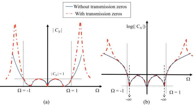
performance of the filtering function with and without a pair of transmission zeros. It can be noted that the magnitude of the filtering function is less than 1 within the passband. The magnitude of the filtering function increases, as the normalized frequency moves away from the passband. Furthermore, if the transmission zeros appear, the magnitude of filtering function grows dramatically.
Figure 2-1. The procedure of the single-band coupling matrix synthesis [90]. INPUT: (1) Filter order(2) Return loss
(3) Prescribed transmission zeros From the recursive technique,the fractional forms of S11and S21are:
S11(Ω) = F(Ω)/E(Ω), S21(Ω) = P(Ω)/(ε E(Ω)), The filtering function is defined as
CN(Ω) = F(Ω)/ P(Ω)
Transfer S-parameters into Y-parameters S11(Ω) = F(Ω)/E(Ω), S21(Ω) = P(Ω)/(ε E(Ω)),
Y11(Ω) = m(Ω)/n(Ω), Y21(Ω) = P(Ω)/ n(Ω),
Y-parameters derived from the transversal coupling matrix are Y11Mand Y
21M. Let
Y11= Y11M,Y
21= Y21M
OUTPUT
14
Figure 2-2. The response of the 3rd order filtering function. (a) The linear scale. (b) The log scale.
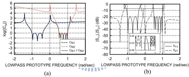
To combine two filtering functions into a composite filtering function and the resulting composite filtering function has to satisfy (2-4), the parallel addition of two filtering functions is applied. The parallel addition of two filtering functions is defined as the reciprocal of the composite filtering function equals to the sum of the reciprocal of two filtering functions just like the total resistance of two parallel connected resistors. After the operation, the filtering function with small value dominants the performance of the composite filtering function. For the filtering function, it has small values within the passband, and very large values while |Ω| > 1, which follows the property of Chebyshev characteristic. Based on above property, while applying parallel addition of two filtering functions with different central frequencies, the dual-band filtering function can be obtained. In Figure 2-3, the solid line represents a dual-band filtering function, which comes from summing up the reciprocal of two 2nd order filtering functions with different central frequencies. In this figure, it is clear to show that the small value of two filtering functions will dominate the value of the composite filtering function. Hence the operation
Ω Ω = 1
Ω = -1
| CN |
| CN | = 1
Without transmission zeros With transmission zeros
Ω log(| CN|)
Ω = -1 Ω = 1
15
of summing up the reciprocal of each filtering function is useful in the dual-band filtering function synthesis.
Figure 2-3. The performance of the 4th order dual-band filtering function.
Based on above description, the composite filtering function can be obtained as follows:
( )
( )
( )
( )
( )
( )
( )
1 2 1 2 1 1 2 2 1 1 2 21
,
1
1
N N N N N N NC
C
C
C
C
C
C
ε ε
ε
ε
ε
ε
ε
Ω
Ω
Ω =
=
Ω +
Ω
+
Ω
Ω
(2-5)where CN1(Ω) and CN2(Ω) are single-band filtering functions with shifted central
frequencies. The principal advantage of this technique is that the individual filtering function CN1(Ω) and CN2(Ω) can be obtained analytically by the efficient recursive
technique and frequency shift. Hence the polynomial of the composite filtering function can be derived as
log(|C
N|)
Ω
Ω= Ω1 Ω=-Ω3 Ω=-Ω4 Ω=Ω2Dual-band filtering function Single-band filtering function #1 Single-band filtering function #2
16
( )
( )
( )
( )
( )
( )
( )
( )
( )
( )
( )
( ) ( )
( )
( )
1 1 2 2 1 2 1 1 2 2 1 2 1 2 2 1 2 1 2 11
1
1
1
,
N N N N N N N N N N N N N N NC
C
C
P
P
F
F
F
F
P
F
P
F
F
P
ε
ε
ε
ε
ε
ε ε
ε
ε
ε
Ω =
+
Ω
Ω
=
Ω
Ω
+
Ω
Ω
Ω
Ω
=
Ω
Ω +
Ω
Ω
Ω
=
Ω
(2-6)where FN1(Ω), FN2(Ω), PN1(Ω), and PN2(Ω) are generated by frequency shifting of the
original filtering function through
( )
(
)
( )
(
)
' ',
,
Ni Ni si Ni Ni siF
F
P
P
Ω =
Ω − Ω
Ω =
Ω − Ω
(2-7)where i = 1 and 2, ωsi is the central frequency for the i-th passband, and F’Ni(Ω) and P’Ni(Ω)
are all generated by recursive technology analytically [93]. In addition, the transmission zeros can be generated using those CN1(Ω) and CN2(Ω) corresponding to their central
frequency at each passband via (2-6).
In case of two passband with different bandwidth, these polynomials should be modified. For the i-th filtering function with frequency shift Ωsi and the multi-band
17
( )
(
)
( )
(
)
, 1 , 12
,
2
,
i i NF Ni si i j j i NF Ni si i j j iF
f
P
p
δ
δ
= =⎛
⎞
Ω =
⎜
⋅ Ω − Ω −
⎟
⎝
⎠
⎛
⎞
Ω =
⎜
⋅ Ω − Ω −
⎟
⎝
⎠
∏
∏
(2-8)where i = 1 and 2, and PNi(Ω) is the denominator and FNi(Ω) is the numerator of CNi(Ω), pi,j
is the jth roots of PNi(Ω) and fi,j is the jth roots of FNi(Ω), and NPi and NFi are the number
of roots of PNi(Ω) and FNi(Ω). The multi-band lowpass domain bandwidths δ1 and δ2 in
(2-8) will be explained in the next section.
The case can be extended to multi-band situation that suppose there are m passbands for a multi-band filter and corresponding filtering function for each passband is CN1,
CN2, …, and CNm so that the composite filtering function can be obtained as
( )
( )
( )
( )
( )
( )
( )
( )
( )
( )
( )
1 1 2 2 1 2 1 1 11
1
1
1
,
N N N m Nm m N N Nm j j m m Ni j Nj i j j i N NC
C
C
C
F
F
F
P
F
F
P
ε
ε
ε
ε
ε
ε
ε
= = = ≠Ω =
+
+ +
Ω
Ω
Ω
⎛
⎞
Ω
Ω
Ω
= ⎜
⎟
⎛
⎞
⎛
⎞
⎝
⎠
⎜
⎟
⎜
⎟
Ω
Ω
⎜
⎜
⎜
⎟
⎟
⎟
⎜
⎝
⎠
⎟
⎝
⎠
Ω
=
Ω
∏
∑
∏
"
"
(2-9)where PNi is the numerator and FNi is the denominator of CNi. Here, each passband has
individual filter order and the number of transmission zeros. By carefully placing the transmission zeros, the requested frequency response can be obtained under desired specifications.
18
S11 and S21 in (2-1), the following equation is used:
( )
( )
( )
( )
( )
( )
( )
, / , / , , N N N N N N N N N N N F Coef P Coef F F F Coef P P P Coef P E j Fε
ε
ε
← × Ω ← Ω Ω ← Ω Ω Ω = + Ω (2-10)where FNCoef and PNCoef are the leading coefficients of FN(Ω) and PN(Ω).
In (2-10), the passivity of the rational function representations of the S-parameters is not guaranteed. To enforce the passivity, those roots of EN(Ω) with positive real part in the
s domain (s = j Ω) are modified by changing the sign of the real parts, as shown in Figure 2-4. Finally, the transversal coupling matrix based on the generated polynomials is obtained using the method in [93].
Figure 2-4. The passivity enforcement for polynomial EN(Ω).
To transfer the response to the bandpass domain, the following equation is used:
Non Passive root Passive root
jΩ
19
1
,
C C H L C C Cf
f
f
f
f
f
f
f
f
f
f
⎛
⎞
Ω =
⎜
−
⎟
−
⎝
⎠
⎛
⎞
=
⎜
−
⎟
Δ ⎝
⎠
(2-11)where Ω is the frequency in the multi-band low-pass domain, f is the frequency in the bandpass domain, fC, fH, and fL are the central frequency, the upper edge of the highest
passband, and the lower edge of the lowest passband in the bandpass domain, respectively, and Δ is the fractional bandwidth.
2.3 Frequency Transformation
The previous procedure to synthesize the multi-band filtering function begins with the filter information in the lowpass domain. The practical specifications, however, are almost described in the bandpass domain. To relate with the information between two domains, here the frequency transformation is provided. Figure 2-5 shows the variables in the bandpass domain and the lowpass domain. In this figure, the relations between variables of the i-th passband in the bandpass domain are shown below:
,
.
iH iL i i i iH iLf
f
f
f
f f
−
Δ =
=
(2-12)20
(
)
(
)
2 2 2 2 4 , 2 4 , 2 , , 1 . i i i i i iH i i i i i iL C 1L 2H 2H 1L C C C f f f f f f f f f f f f f f f f f f Δ + Δ + = −Δ + Δ + = = − Δ = ⎛ ⎞ Ω = ⎜ − ⎟ Δ ⎝ ⎠ (2-12)The requested specifications are return loss (RL), the central frequencies and fractional bandwidths of both passbands in the bandpass domain. The so-called multi-band lowpass domain bandwidth δ1 and δ2 in the Figure 2-5 can be obtained as
,
i iH iL
δ = Ω − Ω (2-13)
where i is the index of the i-th passband.
Figure 2-5. The requested design variables in the bandpass domain and the lowpass domain. RL is the prescribed return loss.
f S11(f) Ω f1L f2H f1 f1Δ1 f2Δ2 fCΔ f2 S11(Ω ) RL RL (2-12) Ω1Η Ω2L Ωc1 Ωc2 Lowpass Domain Bandpass Domain f1H f2L δ1 δ2 fC Ω1L= −1 Ω2H= +1
21
The corresponding transmission zeros in lowpass domain can also be obtained using (2-12). When inserting the transmission zeros in the single-band coupling matrix synthesis procedure [90], the transmission zeros in the single-band lowpass domain should be modified as
(
)
, , , ,2
TZ i j TZ i j ci iP
δ
=
Ω
− Ω
(2-14)where δi is the multi-band lowpass domain bandwidth of the i-th passband, ΩTZ,i,j is the j-th
transmission zero of the i-th passband in the lowpass domain, and PTZ,i,j is the j-th
transmission zero of the i-th passband for inserting into the synthesis procedure in [90].
2.4 Computational Examples
In this section, three examples are used to demonstrate the validation of the proposed synthesis procedure in dual-band filter design. Moreover, prescribed transmission zeros are discussed to be properly described in single-band filtering function.
2.4.1 Example 1: Symmetric Dual-band Bandpass Filter
In this example, the specifications of symmetrical dual-band bandpass filter are provided. Two passbands both are with the filter has filter order 3 and return loss 20 dB. The first passband has a central frequency at 2.32 GHz and 5% fractional bandwidth. The second passband has a central frequency at 2.695 GHz and 5% fractional bandwidth. The transmission zeros are 2.151 GHz, 2.5 GHz, and 2.905 GHz.