國 立 交 通 大 學
電 信 工 程 學 系
博 士 論 文
合成波導之設計與應用
Design and Applications of
Synthetic Waveguides
研 究 生 :吳憲順 (Hsien-Shun Wu)
指導教授:莊晴光 博士 (Dr. Ching-Kuang C. Tzuang)
合 成 波 導 之 設 計 與 應 用
Design and Applications of
Synthetic Waveguides
研 究 生 : 吳憲順 Student: Hsien-Shun Wu
指導教授: 莊晴光 博士 Advisor: Dr. Ching-Kuang C. Tzuang
國 立 交 通 大 學
電 信 工 程 研 究 所
博 士 論 文
A Dissertation
Submitted to Institute of Communication Engineering
College of Engineering
National Chiao Tung University
In Partial Fulfillment of the Requirements
for the Degree of
Doctor of Philosophy
in
Communication Engineering
July 2005
Hsinchu, Taiwan, Republic of China
合 成 波 導 之 設 計 與 應 用
研究生:吳憲順
指導教授:莊晴光 博士
國立交通大學 電信工程學系
摘 要
本篇論文係研究立體式(Three-dimensional)與平面式(Two-dimensional)合成波 導以多層印刷電路板( Multi-layer Printed Circuit Board)製程與矽(Silicon)半導體製 程之實現並提出相關應用。傳統立體式矩形波導(Rectangular Waveguide)可藉由微 小化週期結構 (Periodical Structure)重新合成,並透過成熟之矩形波導轉換器 (Rectangular Waveguide Transition),設計出合成矩形波導(Synthetic Rectangular Waveguide, SRW) 。 經 由 實 驗 與 理 論 相 互 驗 証 , 該 立 體 傳 輸 線 具 備 慢 波 效 應 (Slow-Wave Effects)可突破傳統矩形波導之理論限制,有效縮小面積達 60%以上。 該微小化特性應用到 5GHz 積體化近全向性矩形波導天線 (Omni-directional Rectangular Waveguide Antenna)。更進一步,由於週期結構在能階止帶 (Energy Bandgap) 呈現出完美磁性金屬 (Perfect Magnetic Conductor) 特性,使該立體合成
波導可傳播傳統金屬矩形波導無法存在之第一階横向磁場模(TM10 mode) 而本論
文亦針對該模態提出其模態轉換器 (Mode Converter)。
除外,本論文研究互補式金屬(Complementary-Conducting Strip, CCS)合成波導 在多層結構 (Multi-layer Structure) 之特性與提出相關應用。透過實驗與理論驗 証,互補式金屬在多層結構實現下,除保有原多樣化特徵阻抗合成之特性,亦突 破傳統夾心線 (Stripline)之理論限制,具備更高之慢波因子 (Slow-Wave Factor)。 該 平 面 式 合 成 波 導 以 多 層 印 刷 電 路 板 技 術 , 應 用 在 以 傳 輸 線 為 主 (Transmission-Line based) 之 WLAN 2.4GHz 微小化帶通濾波器設計。而設計出之 濾波器尺寸為 5.0 mm X 5.0 mm X 0.18 mm,甚接近傳統以低溫陶瓷共燒 (Low Temperature Cofired Ceramic)之濾波器體積。
本 論 文 最 後 一 部 份 提 出 平 面 式 合 成 波 導 應 用 於 改 進 傳 統 晶 片 繞 線 電 感 (On-chip Spiral Inductor) 之設計困難。該設計同時以印刷電路板與標準多層 CMOS
Design and Applications of Synthetic Waveguides
Student:Hsien-Shun Wu Advisor:Dr. Ching-Kuang C. Tzuang
Institute of Communication Engineering
National Chiao Tung University
ABSTRACT
This dissertation presents a new class of the transmission lines so-called synthetic waveguide, which can be realized by mass-producible technologies, such as multi-layer print-circuit-board (PCB), and silicon-based monolithic integrated circuit foundry. Meanwhile, the novel design methodologies incorporating the proposed synthetic waveguide are reported to demonstrate the impacts on the designs either in component-level or system-level for meeting the trends of modern portable devices. A new synthetic waveguide, which is the composite structure including the rectangular waveguide transitions and rectangular waveguide synthesized by the periodical electromagnetic bandgap (EBG) structures at top and bottom surfaces of the rectangular waveguide, is theoretically and experimentally verified, showing the following characteristics. First, the slow-wave factor of the synthesized rectangular waveguide (SRW) exceeds the theoretical limit of the conventional metallic rectangular waveguide in the TE10 mode, significantly increasing the size-reduction more than 60%. One
example employing the TE10 mode of the proposed SRW was the design of integrated
waveguide antenna in the 5 GHz ISM band, demonstrating its potential on circuit miniaturization. Second, the proposed SRW can support TM00 and TM10 mode
propagation in the same SRW. Notably, no TM00 and TM10 mode can exist in the
conventional rectangular waveguide with an all-metallic enclosure. Additionally, the waveguide transitions for the synthetic TE10, TM00 mode, and TM10 mode of the SRW
are also presented for the further applications.
The second part of the dissertation focuses on the design and application of the synthetic quasi-TEM transmission line so-called complementary conducting strip transmission line (CCS TL) in multi-layer portion. A series of experimental and theoretical verifications conclude that the stacked CCS TL not only provides a wide design solutions for the circuit requirements but also achieve a low-loss slow-wave
conventional stripline. Moreover, a typical multi-layer system, which includes two filters in different signal layers, is realized by the stacked CCS TL, revealing good isolation between two filters during the system design. Furthermore, the proposed two-dimensional synthetic waveguide is applied to design an transmission-line based 2.4GHz ISM-band bandpass filter for demonstrating a new filter design methodology, which can systematically reducing the size of filter based on multi-layer CCS TL. A quick estimate on the prototype filter with the size of 5.0 mm X 5.0 mm X 0.18 mm reveals that the volume of the prototype approaches that of state-of-the-art device, such as multi-layer low temperature cofired ceramic (LTCC) filters.
Finally, the new spiral inductor architecture, named EBG enhanced inductor, incorporating the synthetic waveguide is presented, providing another solution for designing planar inductors on lossy substrate. The two-dimensional EBG array servers as a ground plane beneath the conventional spiral inductor, providing a shielding for inductor on the lossy substrate. The proposed approach is verified through the experiments using the conventional multi-layer PCB technology and standard 0.25um CMOS foundry, showing that the performance of a spiral inductor can be improved in almost aspects.
誌 謝
在新竹交大的求學生涯是一連串交織著驚喜與酸甜的自我成長。在此謹以誌 謝表達深深地感激對曾經或永遠在我生命中留下痕跡的長輩與朋友。 謝謝莊晴光教授,從開始到現在,我的碩博士學位指導老師,以及他的家人, 師母楊靜蘭女士、小圓、大慶及小萱。教授無私地分享對微波的愛與熱情,精神 上與物質上的全心支持使我的求學舞台得以寬廣與多元。無疑地,教授的身教與 言教更培養學生在面對困難與挫折時應有的心態與方法。曾一同面對連續五次審 稿不過的窘況,也曾享受過一次審稿即過的喜悅。"不輕言放棄,誠實勇敢面對 問題"是教授給學生最好的指導。額外地,師母的金玉良言與近乎完美的烹煮手 藝、善解人意且笑容滿面的小圓、害羞又充滿音樂氣質的大慶與永遠充滿驚奇的 小萱,這些家人們似的溫暖與親情陪我渡過在新竹求學許多週末夜晚。 謝謝楊晃瑞教授,在求學最低潮的時刻成為我的工作夥伴,為人生與工作帶 來全新的體驗。爽朗的笑聲、感性的眼神與充滿生活藝術的言談最令人欣賞;工 程上的精準、系統化的做事原則與高效率的執行力最令人敬佩。學生感謝有此緣 份能與長輩工作、向長輩學習。 謝謝彭勁融工程師,從開始到現在,陪伴我在新竹整整七年時光。雖然各自 的專業背景不同,亦所屬在不同的工作崗位;然感受到的是另一股對工作的投入 與解決困難時的執著冷靜。有著不同的生活習慣與人生看法,這二仟多個相處日 子裡,回味無窮。 謝謝毫米波體積電路實驗室的歷任助理,從開始到現在,李苑佳小姐、楊惠 玲小姐、陳郁萍小姐和她們天真無邪、活力無窮的小朋友們。與專業秘書共事, 從日常做人處事的小細節、面對決策時的多方思考與評估、對上司、同僚與下屬 的聯絡與溝通都使晚輩見識到事情的推動不全然僅有技術或學理,協調與管理更 是最後的關鍵。 懷念毫米波體積電路實驗室的所有成員。從開始到現在,國丞學長、正南學 長、學達學長、經國學長、宣仲學長、耀德學長、國峰學長、毓喬學長、多柏學長、嘉振學長、佐政學長、才弼、韶正、振榮、昌毅、慈惠、文翌、博議、文昶、 鶴中、美蒨、竟谷、佳民、嘉良、智閔、書豪、揚裕、俊甫、繼禾與憲宏。曾一 起相處的時光,有笑有淚、有甘有苦,希望有機會能再相聚。 謝謝全家人無止盡的關懷與支持。謝謝體諒我求學時少回家、少聯絡與晚 歸。點點滴滴的付出雖不易察覺但意義與影響卻最深遠。謝謝未曾間斷且無所求 的栽培,從最開始到現在,讓我無顧慮地完成所有學業並在最重要的時刻見證我 的成長。謝謝永不變的贊美與叮嚀,使我面對挫敗時快快站起、面對成功時更能 精益求精。 謝謝好朋友的幫助與溫暖的照顧。俊麟即時的線上咨詢與偶爾的探望、秀宜 淡淡的問候與來信、涵秦小姐親切的叮嚀與協助、玉琇家姐般的照顧與驚奇的小 禮物、珍儀逗趣的照片、貼心的手工皂與自製的護唇膏。讓我這一路走來,不曾 孤單。 謝謝潛力無限的台大伙伴。孟儒、王珅、安錫、思賢、瑞琦、啟揚、昆宏、 致嘉與彥翔。在求學的最後階段相互的交流與幫助,讓我在不同的環境下學習與 成長,體驗到不同的學風與團體生活。 我繼續認真的學習,在台北、新竹與世界各地, 你投射過來關注的眼神, 詫異也好, 欣賞也罷, 或許引起我的目光 希望使你注意的 不是那稚嫩的臉龐, 而是我追求卓越的心 順子
TABLE OF CONTENTS
ABSTRACT (Chinese)……….I ABSTRACT (English)……….II ACKNOWLEDGMENTS...IV TABLE OF CONTENTS………..………VI LIST OF TABLES………...VIII LIST OF FIGURES………...IX CHAPTER 1 Introduction…………..………...1 1.1 Background………...11.2 Reviews of Synthetic Waveguides………...4
1.3 Organization……….……....8
CHAPTER 2 Integrated Synthetic Rectangular Waveguide……….……...8
2.1 Synthetic Rectangular Waveguide: Design and Operation Principles………...12
2.1.1 Dispersion Characteristics of Parallel-Coupled electromagnetic Bandgap (EBG) Surfaces………..13
2.1.2 Simplified Rectangular Waveguide Models for SRW………....19
2.2 Synthetic Rectangular Waveguide: Waveguide Transitions to Planar Transmission Lines, and De-embedding Studies………...14
2.2.1 Integrated Synthetic Rectangular Waveguide (SRW)……….21
2.2.2 Single-Mode Approximate Algorithm for De-embedding Integrated Synthetic Rectangular Waveguide (SRW)……….27
2.3 TE10 Mode Synthetic Rectangular Waveguide (SRW)………..34
2.4 TM00 and TM10 Mode Synthetic Rectangular Waveguides (SRW)…………...40
2.5 TE10 Mode Miniaturized Integrated Rectangular Waveguide Antenna……….51
2.5.1 Radiation Characteristics of Miniaturized Synthetic Rectangular Waveguide (SRW) Antenna………...57
CHAPTER 3 Multi-layer Synthetic Quasi-TEM Transmission Line………63
3.1 Multi-layered Complementary Conducting Strip Transmission Line………....64
3.2 Experimental Filter Design Procedure………...73
3.2.1 Transmission Line Filter: General Description………...73
3.2.2 Design Procedure of Transmission Line Bandpass Filter………...80
3.3 Miniaturized Transmission-Line Bandpass Filter: Layout and Measurements.85 3.4 Discussion………..93
CHAPTER 4 EBG Enhanced PCB / Monolithic Spiral Inductors………99
4.1 Guiding Characteristics of the Microstrip line on the EBG Ground Plane…..100
4.2 Equivalent Model for the Rectangular Spiral Inductor………106
4.3 EBG Enhanced-Inductor………..110
4.3.1 EBG Enhanced Laminated Spiral Inductor………...110
4.3.2 EBG Enhanced Monolithic Spiral Inductor………..118
CHAPTER 5 Conclusion……….133
5.1 Contributions………....133
5.2 Future Works………....135
APPENDIX I Simplified Waveguide Models for Synthetic Rectangular Waveguide (SRW)……..………..137
APPENDIX II Volume Estimation for Transmission-Line Based Bandpass Filter Incorporating Multi-layer Complementary Conducting Strip Transmission Line (CCS TL)………..143
APPENDIX III Equivalent Transmission-Line Model for Spiral Inductor…...145
LIST OF TABLES
Table 2.1 Theoretical Q-factor of the TM00 mode SRW at 11.0 GHz………..49
Table 2.2 Theoretical Q-factor of the TM10 mode SRW at 11.4 GHz………..50
Table 2.3 All-metallic rectangular waveguide with different cutoff frequencies…….50 Table 3.1 Variables for Volume Estimation of Proposed Bandpass Filter………94
LIST OF FIGURES
Figure 1.1 Development trends of Synthetic Waveguide……….………..5 Figure 2.1 Rectangular waveguide structures (a) using all-metallic enclosure, (b) top
and bottom surfaces incorporating perfect magnetic conductor (PMC) (c) proposed SRW, (d) EBG unit cell applied in SRW………15 Figure 2.2 Brillouin diagram of the two-dimensional periodical array made of unit cell
of Fig. 2.1 (d)………..18 Figure 2.3 TE10 mode SRW including microstrip-to-waveguide transitions (a) top
view, (b) front view (c) side view………...24 Figure 2.4 TM00 mode SRW including slotline-to-waveguide transitions (a) top view,
(b) front view, (c) side view………...25 Figure 2.5 TM10 mode SRW including CPW-to-waveguide transitions (a) top view, (b)
front view, (c) side view……….26 Figure 2.6 Proposed de-embedding procedures for extracting guiding characteristics
of the planar rectangular waveguide………..29 Figure 2.7 Validity check of the proposed de-embedding method for extracting
rectangular waveguide parameters: (a) |S21| (b) ∠S21 (c) |S11| (d) ∠S11….30
Figure 2.8 Comparison of the extracted normalized phase constants of the conventional rectangular waveguide with those obtained by exact equation: (a) phase constant, (b) Q-factor………..33 Figure 2.9 Measured/Simulated two-port S-parameters of TE10 mode synthetic
rectangular waveguide (SRW) parameters (a) |S21| (b) ∠S21 (c) |S11| (d)
∠S11………36
Figure 2.10 Comparison of the extracted normalized phase constants of the TE10
mode SRW with those obtained by HFSSTM simulation: (a) phase constant, (b) Q-factor……….37
Figure 2.11 Field distribution of the synthetic TE10 mode rectangular waveguide at 6.0
GHz (a) 2D Ey-field (b) 2D Hx-field (c) 2D Hz-field………..39
Figure 2.12 Scattering analyses of the integrated SRW with various waveguide transitions (a) TM00 mode converter (b) TM10 mode converter………….42
Figure 2.13 Normalized phase constants of the proposed synthetic TM00 and TM10
mode rectangular waveguides………43 Figure 2.14 Field distribution of the synthetic TM00 mode SRW at 11.0 GHz (a) 2D
Ex-field (b) 2D Hy-field………..45
Figure 2.15 Field distribution of the synthetic TM10 mode rectangular waveguide at
11.4 GHz (a) 2D Ex-field (b) 2D Hy-field (c) 2D Ez-field………..47
Figure 2.16 Miniaturized synthetic rectangular waveguide (SRW) antenna (a) top-view. (b) side-view. (c) front-view………...53 Figure 2.17 Normalized phase constant of the proposed TE10 mode synthetic
rectangular waveguide (SRW)………54 Figure 2.18 Photograph of the miniaturized synthetic rectangular waveguide (SRW)
antenna. (a) top-view. (b) bottom-view………..59 Figure 2.19 The measured result of the input reflection coefficient for the miniaturized synthetic rectangular waveguide (SRW) antenna………...60 Figure 2.20 Far-field radiation patterns of the proposed synthetic rectangular
waveguide antenna at 5.25GHz: (a) E-plane, (b) H-plane, (c) cross-polarization………...62 Figure 3.1 Unit cells of complementary conducting strip transmission line (CCS TL):
(a) For series connection. (b) For bent connection……….66 Figure 3.2 Synthetic complementary conducting strip transmission line (CCS TL): (a) Meandered CCS TL. (b) Sandwiched meandered CCS TL………...67 Figure 3.3 The guiding characteristics of the sandwiched CCS TL and the
conventional stripline: (a) real part of characteristic impedances, (b) normalized phase constants………69
Figure 3.4 Multi-function module incorporating four-layer meandered CCS TLs. (a) Frequency responses of 2.4 GHz LPF in M1 and M2 metal-layers. (b) Frequency responses of 2.4 GHz BPF in M2, M3 and M4 metal-layers. (c) Measured transmission coefficient between LPF and BPF in four-layer CCS TLs configuration………..71 Figure 3.5 Transmission-line TL bandpass filter (BPF) with identical shunt stubs: (a)
equivalent circuit model, (b) simulated frequency responses………75 Figure 3.6 Transmission-line TL bandpass filter (BPF) with un-symmetrical shunt
stubs: (a) equivalent circuit model, (b) simulated frequency responses…76 Figure 3.7 Transmission-line TL bandpass filter (BPF) with symmetrical shunt stubs:
(a) equivalent circuit model, (b) simulated frequency responses………...79 Figure 3.8 Parallel resonators: (a) Lumped realization (b) Distributed realization…..81 Figure 3.9 Characteristics of input susceptance of transmission-line parallel
resonator ………...82 Figure 3.10 Brief description of the transmission-line bandpass filter design: (a)
Lowpass prototype, (b) Conversion of series inductors to shunt capacitors, (c) Lowpass to bandpass transformation, (d) transmission lines approximations of parallel resonators and J inverters………84 Figure 3.11 Three-dimensional view of transmission-line bandpass filter realized by
multi-layer complementary conducting strip (CCS) transmission line (TL)...87 Figure 3.12 Experimental setups for measuring miniaturized BPF……….89 Figure 3.13 Measured results of miniaturized bandpass filter……….90 Figure 3.14 Photograph of 2.4 GHz miniaturized bandpass filter on one Euro (€1)...92 Figure 3.15 A Survey of 2.4 GHz ISM band bandpass filter in size (volume) and
thickness………...97 Figure 4.1 The microstrip line on the EBG ground plane: (a) three-dimensional view,
(b) multi-layer EBG ground plane, (c) cross-section view of the multi-layer configuration………..102
Figure 4.2 Characteristics of the microstrip line on the uniform ground plane and EBG ground plane: (a) complex propagation constant, (b) characteristic impedance………...105 Figure 4.3 The equivalent models for the rectangular spiral inductor: (a) lumped
model, (b) transmission line model………108 Figure 4.4 Spiral inductors on different ground planes; h1=h3=0.2 mm, h2=0.05 mm,
Gx=Gy=5.0 mm, Lx=Ly=3.0 mm, S2=0.2 mm, w2=0.2 mm. (a) spiral inductor
on the uniform ground plane, (b) spiral on the EBG ground plane…………112 Figure 4.5 Equivalent transmission line parameters of the PCB spiral inductor on the
uniform ground plane and EBG ground plane: (a) complex propagation constant, (b) characteristic impedance………...115 Figure 4.6 Measured results for comparing EBG inductor with conventional spiral
inductor applying the multi-layer PCB fabrication: (a) series inductances (Ls),
(b) series resistance (Rs), (c) parasitic resistance (Rp), (d) parasitic capacitance
(Cp), (e) quality factor (Q)………..117
Figure 4.7 Simplified cross-section view of the 0.25um 1P5M CMOS process…...122 Figure 4.8 Photograph of the EBG enhance monolithic spiral inductor fabricated using
CMOS 0.25um process………..123 Figure 4.9 Histograms of the inductor Q-factors over 12 samples: (a) EBG ground
shield inductor (EBG-GS), (b) conventional inductor with no ground shield (NGS)……….126 Figure 4.10 Equivalent transmission line parameters of the monolithic spiral inductor
on the uniform ground plane and EBG ground plane: (a) complex propagation constant, (b) characteristic impedance………...127 Figure 4.11 Measured results for comparing EBG inductor with conventional spiral
inductor applying the 0.25um CMOS process: (a) series inductances (Ls), (b)
series resistance (Rs), (c) parasitic resistance (Rp), (d) parasitic capacitance
(Cp), (e) quality factor (Q)………..131
CHAPTER 1
Introduction
1.1 Background
Portable wireless devices have evolved into the convergence realm, integrating multi-frequency and multi-standard protocols. One key factor for such success of wide acceptance is the miniaturization of wireless apparatus. The continuing improvement of semiconductor processes, shrinking photolithography, and multi-layer integration technologies such as the low temperature cofired ceramics (LTCCs) and printed circuit boards (PCBs) lead the continuing technological development in system-on-chip (SOC) and system-in-package (SIP) [1-7]. Although as many as possible wireless building blocks have been integrated into SOC, the radio frequency (RF) front-end module (FEM) and other devices are mostly in discrete forms or embedded into the SIP. A complete solution for making a wireless device with a very small form factor is becoming a reality by combining advanced techniques of SOC and SIP.
On the other hand, closely examining the integration scheme of the FEM, the functional blocks, including antenna, filter, balun, etc., and various transmission lines which are designed based on different circuit principle and realized by different
technologies, may require additional transitions to establish the smooth interfaces between the adjacent building blocks. Additionally, two kinds of transmission lines, which are connected, require the mode converter for the energy transformation. Those transitions and mode converters also become an important part during the components design and seriously dominate the performance and appearances of the FEM.
In the Year 2000, a new design methodology so-called the advanced coplanar strips system (ACSS) was proposed for in millimeter-wave module and RFIC designs [8]. The ACSS is a system of guiding structures embedded in a multilayered printed-circuit environment such as print circuit board (PCB) and low temperature cofired ceramics (LTCC) for RF system-on-chip (SOC) design. The ACSS millimeter-wave transceiver module, which incorporates typical PCB process for making all-in-one module, has demonstrated all aspects of planar realizations of antennas, antenna arrays, resonators, filters, mixers, oscillators and packages [9]. The ACSS exploits the multi-layered guiding system into the unprecedented domain, which creates new approaches for RFIC design and module integration. The unprecedented domain is best described by the concepts of the synthetic waveguides in which most popularly known guiding modes such as planar (microstrip), quasi planar (CB-CPW), non-planar (rectangular waveguide) structures propagate freely in the multi-layered ACSS system with a little increasing of propagation losses or
transition losses.
In the 2005 international microwave conference (IMS2005), the transmission line community organized a section titled “Synthetic Transmission Lines and Their
Applications”, revealing the trends of the researches on synthetic waveguides [10-14].
This special section demonstrated a single processing technology, achieving unprecendted guiding characteristics such as high slow-wave factor, wide solutions of characteristic impedance syntheses, and build-in transitions for the system integrations. The efforts organized by IMS2005 sub-community faithfully reflected the contributions of this dissertation undertaken in the past six years. Perhaps on e best notion on the synthetic waveguide could be quoted from an invited speech at City University of Hong-Kong in July 2004, when Professor Ching-Kuang C. Tzuang gave a seminar on the synthetic waveguide and its applications to the RF SOC and SIP designs. This dissertation covers all aspects of the synthetic waveguide as quoted above.
Incompatible guiding structures, which are conventionally made by different technologies, are blended into a mass-producible technology or new waveguide structures that exhibit extraordinary characteristics, behaviors, and merits using the same mass-producible technology belong to the domain of synthetic waveguide.
1.2 Review of Synthetic Waveguides
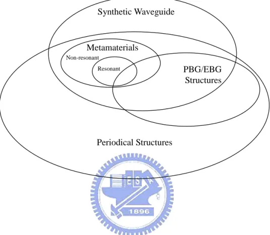
Fig. 1 shows the developing trends of the synthetic waveguide in the past ten years. An amount design of the synthetic waveguides is involved with the periodical structures, which can be classified by photonic bandgap (PBG), electromagnetic bandgap (EBG), Metamaterials, and etc.. One example of designing synthetic waveguide with periodical structure is proposed by Itoh et al. in 1998 [15].
The microstrip line incorporating the uniplanar compact photonic bandgap (UC-PBG) ground plane become a new slow-wave device. Additionally, this new slow-wave transmission line, which differs from the thin-film transmission lines reported from 1970 to 1993, can achieve small attenuation constant less than one dB per guiding wavelength [16]. Such synthetic waveguide is realized by the conventional print circuit board (PCB) technology and had been demonstrated its wide applications on the microwave active and passive circuits, including improvement of power amplifier efficiency, and bandpass filter design with wide-band rejection [17].
Fig. 1.1 Development trends of Synthetic Waveguide. Synthetic Waveguide PBG/EBG Structures Periodical Structures Metamaterials Non-resonant Resonant
Another example of synthetic waveguide incorporating with periodical structure is reported by Tzuang et al. in 2001 [18]. The signal trace of the conventional microstrip consists of the coil-coupled electromagnetic bandgap (EBG) cells, revealing electric, magnetic and electric properties along the transverse plane of the microstrip line [16]. The modal behavior of the electric-magnetic-electric (EME) microstrip line had been carefully investigated, revealing the first high-order mode of EME microstrip line can be controlled and synthesized in different frequencies. Such new modal behavior is also applied to design a dual-band leaky wave antenna [19].
On the other hand, the synthetic waveguides, which can be synthesized to exhibit the negative permittivity and permeability, are classified as the metamaterials. Metamaterials are commonly referred to as left-handed (LH) transmission lines because of their unique guiding characteristics such as the reversal of Snell’s Law, the Doppler effect, and the VavilovCerenkov effect, which is the radiation produced by a fast-moving particle as it travels through a medium [20].
The idea of left-handed (LH) transmission line was first presented by the Russian physicist Veselago in 1967. Veselago theoretically showed that the electric field, magnetic field, and wavevector of an electromagnetic wave in an LH transmission line form a left-handed triad. Therefore, LH transmission lines support energy propagation with group and phase velocities that are antiparallel, a phenomenon
which is associated with negative index of refraction [21]. The experimental verifications of metamaterials were performed by the Smith et. al in 2001 [22]. During the experiments, the metamaterial was realized by a wedge-shaped two-dimensional periodical array consisting of the magnetic resonator so-called split-ring resonators (SRRs) and thin conducting wires. The periodical array was excited by the plane wave and the wavefront of the transmission wave traveled backward toward the incident wave, confirming the existing of negative index of refraction [22]. Parallel to the findings of Smith, the planar LH transmission line based on SRRs is also reported in the very recently [23-24].
On the other hand, the composite right/left hand (CRLH) transmission line (TL) realized by the non-resonant elements is also reported by Itoh et al. [25]. The characteristics of CRLH TL have been investigated by the transmission line theory and its guiding properties are modeled by a lossless LC network. Furthermore, the development of equivalent LC network, which consists of shorted shunt stubs and series inter-digital capacitors, is also presented [26]. Both theoretical and experimental results show that the CRLH TL can propagate the electromagnetic wave with the right-handed and left-handed triads alternatively [27]. Many applications based on CRLH TL are also reported for demonstrating the capability of such new planar synthetic waveguide [28-32].
This dissertation focus on the development of synthetic waveguides which have three main features: 1) Compact circuit design is compared to those based on popularly known guiding structures, 2) High Q-value of the guiding structure is maintained or much better than the conventional guides, and 3) practical realization is based on the existing technologies without any modifications.
1.3 Organization
The first kind of synthetic waveguide, presented in Chapter 2, is named synthetic rectangular waveguide (SRW). The SRW, which is consist of two electrical sidewalls and two parallel periodical structures placed at top and bottom surfaces of the waveguide, is made by multi-layered integrated circuit processes with large ratios of SRW lateral dimensions to substrate thickness. The two-dimensional periodical structures comprise unit cells made of coupled coils; show a slow-wave region for the lowest band and a stopband region above the slow-wave region. Chapter 2 reports both theoretically and experimentally that combining the two distinct regions of propagation of two-dimensional periodical structures leads to the design of a SRW that simultaneously exhibits the following unique characteristics. First, the slow-wave factor of the particular SRW significantly exceeds the theoretical limit of εrfor the
conventional metallic rectangular waveguide in the TE10 mode. Second, SRW can
TM00 and TM10 mode can exist in the conventional rectangular waveguide with an
all-metallic enclosure. Third, the Q-factor of the SRW is high in TE10 mode, TM00
mode, and TM10 mode for the particular case study. Fourth, the waveguide transitions,
including the tapered microstrip, the finline, and tapered coplanar waveguide (CPW), are integrated with the SRW in the same polymer substrate for the synthetic TE10,
TM00 mode, and TM10 mode converters, respectively. One example employing the
TE10 mode of the proposed SRW was the design of miniaturized four-slot antenna
array in the 5 GHz ISM band to demonstrate the compact appearance, high antenna gain using a conventional FR4 substrate.
Chapter 3 presents the second kind of synthesized waveguide named stacked complementary conducting strips (CCS) transmission line (TL). Notably, CCS TL was reported recently to be an effective means of miniaturizing microwave circuits [33]. However, in this dissertation, the stacked CCS TLs, which are separated by a meshed ground plane in a multi-layer print-circuit-board (PCB) structure, are introduced for the first time. A practical example is employed to verify the isolation, showing a high level of satisfactory with negligible effects on desired circuit performances. Furthermore, the proposed artificial transmission line is applied to the design of a 2.4 GHz ISM-band bandpass filter prototype of a size that approaches that of state-of-the-art device. The application of the stacked CCS TL results in the
filtering of almost nearly the same volume as the number of substrates is increased. A designer can therefore optimize the area and thickness required for product integration. A quick estimate of the miniaturized filter design based on stacked CCS TL shows that the particular filter prototype approaches the process limit.
Chapter 4 explores the application of synthetic waveguide to the design of PCB and monolithic spiral inductor. The microstrip on the electromagnetic bandgap (EBG) ground plane has been experimentally verified, showing that the increasing characteristic impedance and reducing propagating loss of the synthetic waveguide can be established simultaneously for the operation frequency below the first stopband, leading to the design of a new inductor configuration or the so-called EBG enhanced inductor. The EBG enhanced inductor consists of a two-dimensional electromagnetic bandgap (EBG) periodical array beneath the conventional spiral inductor. A physical model is presented to investigate both characteristics and physical insights of the proposed inductor architecture. Both laminated and monolithic spiral inductors are designed and tested to demonstrate that the performance of the spiral inductor can be improved in almost aspects by placing the EBG ground plane beneath the spiral inductor.
Chapter 5 summarizes the contributions of the dissertation and identifies the future works.
CHAPTER 2
Integrated Synthetic Rectangular Waveguide
In this chapter, the first find of synthetic waveguide, named synthetic rectangular waveguide (SRW), is presented. An SRW, which is made of two laminated two-dimensional (2D) periodical structures and a substrate sandwiched between the 2D structures. The SRW is made by multi-layered integrated circuit processes, which typically have large ratios of SRW lateral dimensions to substrate thickness. Theoretical investigations of the periodical structures show that the corresponding Brillouin diagram have the lowest band of normalized propagation constant much higher than the square root of the relative dielectric constant εr of the substrates.
Application of the dispersion characteristics of the two-dimensional periodical structures coupled with appropriate mode converter designs leads to results in SRW designs supporting TE10, TM00 and TM10 modes.
Section 2.1 shows the slow-wave and high-impedance-surface behaviors of the two-dimensional periodical structures. Additionally, a simplified behavior model for the SRW is also presented for predicting the various modal behaviors in the SRW. Section 2.2 describes the de-embedding procedures to remove the effects of the mode converters necessary to interface the SRW to external measurement ports for TE10,
TM00 and TM10 modes. The de-embedded data are applied to validate the results
obtained by the finite element method (FEM). Section 2.3 reports the newly TE10
mode SRW with a cutoff frequency that is much lower than that of the all-metallic rectangular waveguide based on the same structural and material constants; the slow-wave factor of the TE10 mode SRW is also significantly greater than εr, which is
the theoretical limit of a conventional rectangular waveguide. εr is the relative
dielectric constant of the PCB substrate. Section 2.4 investigates the propagations of TM00 and TM10 modes of the same SRW. Notably, no TM00 and TM10 mode can exist
in the conventional rectangular waveguide with an all-metallic enclosure. Finally, one example, which employs the TE10 mode of the proposed SRW for designing a
four-slot waveguide antenna in the 5 GHz ISM band, is presented in Section 2.5. The antenna is built and tested, showing the gain of 4.28 dBi, 60 percent area reduction in waveguide cross-section, measuring 71.0 mm x 10.5 mm x 0.9 mm (including the microstrip-to-waveguide transition) on a conventional FR4 (εr=4.1) substrate.
2.1 Synthetic Rectangular Waveguide: Design and Operational Principles
Figure 2.1(a) illustrates the conventional rectangular waveguide made using four smooth metal plates. If the top and bottom metal plates are replaced by perfect magnetic conductors (PMC) as shown in Fig. 2.1(b), the guiding characteristics of the
conventional rectangular waveguide are drastically changed. This paper presents a new approach for designing integrated rectangular waveguides. As illustrated in Fig. 2.1(c), the integrated synthetic rectangular waveguide (SRW) consists of two vertical plated sidewalls and two EBG surfaces replacing the top and bottom plates of Fig. 2.1(a). The proposed SRW can support propagating modes in both rectangular waveguides as shown in Figs. 2.1(a) and (b). The SRW extensively applies the propagation characteristics of periodical structures.
2.1.1 Dispersion Characteristics of Parallel-Coupled Electromagnetic Bandgap (EBG) Surfaces
In the SRW, the two-dimensional periodical array, or the so-called EBG surface, constitutes both top and bottom metallic surfaces of the conventional rectangular waveguide. Figure 2.1 (d) details the unit cell design of the EBG surface. The unit cell consists of a pair of connected spiral coils; one is located at the top surface and the other at the bottom surface. The connected spiral coils are DC-connected by a through-hole at the center. The spiral coils form coupled inductors, and the overlapped area between the spirals creates additional capacitances. Furthermore, inductive and capacitive couplings also exist between adjacent cells. Thus the propagation characteristics of the periodical structure are highly dispersive. The full-wave finite-element-based simulation package HFSSTM is applied to obtain the dispersion
characteristics of the multi-layered two-dimensional periodical structure of Fig. 2.1(d). In the numerical investigation, two pairs of master-slave boundaries of assumed phase differences were placed at four edges of the unit cell to compute a corresponding complex frequency of the eigenvalue, from which the phase and attenuation constants (γ=β-jα) of the two-dimensional periodical structure were obtained [33].
b a εr, µr PEC PEC PMC PMC X Y X Y t1 t2 t3 via εr a b X Y b a PEC PEC PEC PEC εr, µr D1 Lt Lb Lt Lb W S D2 X Z t1 t3 t2 (a) (b) (c) (d)
Fig. 2.1 Rectangular waveguide structures (a) using all-metallic enclosure: a = 7.0 mm, b = 0.609 mm, εr = 3.38, tanδ = 0.0035, (b) top and bottom surfaces
incorporating perfect magnetic conductor (PMC) (c) proposed SRW: t1 = t2 = t3 =
0.203 mm (d) EBG unit cell applied in SRW: W = 0.2 mm, S = 0.2 mm, D1 = 0.25
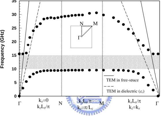
Perfect matching layers (PMLs) were placed adjacent to the top and bottom surfaces of the unit cell with to absorb the radiated waves. Figure 2.2 plots the corresponding Brillouin diagram of the EBG cell. The straight solid (dashed) lines represent the propagation of the transverse electromagnetic (TEM) mode in free-space (dielectric medium with relative permittivity of εr). These straight lines form two
triangles, as shown in Fig. 2.2. The region outside the solid triangle belongs to the radiation zone. Inside the solid triangle, however, is the bound mode region. In this case study, predominant TEM solutions were observed inside the triangle formed by the dashed lines for operating frequencies below 9.85 GHz, manifesting the slow-wave factor greater than εr , which is the upper ceiling for most conventional
guided-wave structures. The electric (magnetic) fields are mostly perpendicular (parallel) to the spiral coils and negligible field components are observed along the direction of propagation. Near zero operating frequency, the phase constant asymptotically approaches that of the TEM mode in the dielectric medium with εr.
Near 9.85 GHz, the group velocity approaches zero. The magnitude of the modal currents near cutoff becomes much smaller than that of the predominant TEM mode at 5.0 GHz. Above 15 GHz, predominant TE mode solutions were observed, since, electric fields exist only in the plane transverse to the direction of propagation. Thus the TE mode is designated as the first high-order mode of the periodical structure
shown in Fig. 2.1 (d). Below 9.85 GHz, the EBG periodical structure is a slow-wave guiding structure, establishing the core operational principle for designing miniaturized integrated SRW.
Equally importantly that the Brillouin diagram shows a broad spectrum of forbidden band between 9.85 and 15.0 GHz. Such stopband connected to the high impedance surface, or the so-called magnetic surface, had been extensively studied [34-35]. Thus the SRW of Fig. 2.1(c) seems to exhibit guiding properties closely resembling those of Fig. 2.1(b) in the forbidden band. In the passband below 9.85 GHz, however, the SRW is more like the conventional rectangular waveguide shown in Fig. 2.1(a).
0 5 10 15 20 25 30 35 40 0 5 10 15 20 25 30 35 Frequency (GH z ) Γ kx=0 N M Γ kzLz/π kxLx/π kz=π/Lz kxLx/π kz=kx TEM in free-space TEM in dielectric (εr) Γ N M
Fig. 2.2 Brillouin diagram of the two-dimensional periodical array made of unit cell of Fig. 2.1 (d).
2.1.2 Simplified Rectangular Waveguide Models for SRW
As mentioned above, electromagnetic bandgap (EBG) surfaces, which form both top and bottom layers of the synthetic rectangular waveguide (SRW), behave like magnetic walls (electrical walls) in the stopband (passband). Therefore, Figs 2.1 (a) and (b) represent simplified rectangular waveguide models of the SRW. Since the proposed SRW is realizable by multi-layered integrated circuit processes, the lateral dimensions (along the x-axis) of the SRW are typically much larger than the thickness of the substrate along the y-axis. Consequently, the lowest order TE modes of Fig. 2.1(a) are TE10, and TE20, etc., whereas the lowest TM modes of Fig. 2.1(b) are TM00,
and TM10, etc. TM00 mode is essentially a TEM mode with uniform transverse Ex and
Hy fields in the waveguide cross-section, which manifests the TEM mode waveguide
as reported by D. Sievenpiper et. al [36], T. Itoh et. al [35], and Per-Simon Kildal et. al [37], respectively. The procedures for deriving the solutions of TEn0 modes are
well-documented [38]. The same procedures are also applied to investigating the TMm0 modes of idealized SRW. For TEn0 modes: r r c ω k = ε µ (1),
relative permeability µr. ,... 3 , 2 , 1 , ) ( 2 2 − = = n a n k n π β (2),
where n represents order of the TE mode and a is the lateral dimension of SRW in x-direction. The lowest order mode is the TE10. Only three field components exist for
the TEn0 mode, namely,
z n β j r y jωµ µ aH naπ x e E =− 0 0sin( ) − , (3) z n β j x a x e π n aH β j H = 0sin( ) − , and (4) z n β j z x e a π n π n H H = 0 cos( ) − . (5)
The TEn0 mode has a cutoff frequency strictly related to lateral dimension a, order n,
and material constants, i.e.,
r r cutoff a nc f n µ ε 2 0 TE , = (6) For TMm0 modes: ,... 2 , 1 , 0 , ) ( 2 2 − = = m a m k m π β (7),
where m represents order of the TM mode and a is the lateral dimension of SRW in x-direction. The lowest order mode is the TM00, which is the zero-cutoff limit of TM
z m β j r y a x e m aE ε ωε j H =− 0 0cos( π ) − (8) z m β j m x x e a π m aE β j E =− 0cos( ) − (9) z m β j z a x)e m ( π m E E = 0 sin π − (10)
The TMm0 mode has a cutoff frequency strictly related to lateral dimension a,
order m, and material constants, i.e.,
r r cutoff a mc f m ε µ 2 0 TM , = (11)
It is interesting to notice that the interchange of E and H, sine and cosine leads to the interchange of TEn0 and TMm0 modes. Additionally, the SRW shows different
dispersion characteristics from those of idealized TEn0 and TMm0 modes. In the later
sections, we will show that the TM00 mode of the SRW has a cutoff frequency and
that both TE10 and TM10 modes have different cutoff frequencies, not dictated by (6)
and (11).
2.2 Synthetic Rectangular Waveguide: Waveguide Transitions to Planar
Transmission Lines, and De-embedding Studies
2.2.1 Integrated Synthetic Rectangular Waveguide (SRW)
As shown in Fig. 2.1 (c), the synthetic rectangular waveguide (SRW), was formed on a RO4003TM printed circuit board (PCB) with a relative dielectric constant of 3.38 and a tanδ of 0.0035. The metal printed on the substrate was copper with a thickness
of 17 µm. Notably, the electromagnetic bandgap (EBG) surface comprised four unit
cells in the transverse direction of the SRW. Similar design had been reported and applied in designing the dual-band leaky-mode antenna [39], indicating that the design of the EBG surface shown in Fig. 2.1(c) has stopband characteristics similar to those two-dimensional arrays of infinite number of cells.
The propagating energy of the synthetic rectangular waveguide (SRW) must be interfaced to planar guiding structures to become a useful integrated guiding device. This section describes various designs to interface SRW supporting TE10, TM00, and
TM10 modes. A streamline mode converter made of a tapered microstrip has been
successfully demonstrated as a good waveguide transition device to interface a microstrip line and a rectangular waveguide supporting TE10 mode [40-44]. The
E-field of this tapered microstrip mode resides mostly in the transverse y-direction in the same way the TE10 mode does, thus ensuring smooth field transition in the mode
converter. Parts (a), (b), and (c) of Fig. 2.3 show top, front, and side views of a back-to-back connected SRW supporting TE10 mode with interfaces to two external
microstrip ports.
Resorting to (9) the TM00 mode exhibits a constant E-field polarization in the
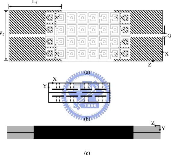
x-direction, suggesting a symmetric perfect electric conductor (PEC) plane at x = a/2. Therefore, a tapered finline inserted on the horizontal plane of y = b/2 is proposed for
the TM00 SRW waveguide transition as illustrated in parts (a), (b), and (c) of Fig. 2.4.
Likewise a tapered finline is the waveguide transition for TM00 mode SRW. Figure 2.5
illustrates how a tapered CPW, which is symmetrical about a perfect magnetic conductor (PMC) surface at x = a/2, works as a TM10 mode converter.
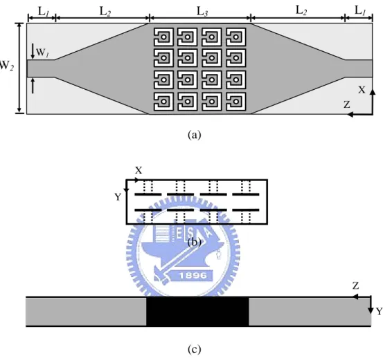
L1 L2 L3 L2 L1 W2 X Z W1 X Y (a) (b) (c)
Fig. 2.3 TE10 mode SRW including microstrip-to-waveguide transitions (a) top view:
L1=3 mm, L2=8 mm, L3=7.2 mm, W1=0.8 mm, W2=7 mm, (b) front view: waveguide
thickness (y-axis) = 0.609 mm, (c) side view.
Z
X Y
(a)
(b)
(c)
Fig. 2.4 TM00 mode SRW including slotline-to-waveguide transitions (a) top view: G1
= 0.15 mm, L4 = 13.05 mm, (b) front view: waveguide thickness (y-axis) = 0.609 mm,
(c) side view. W2 G 1 X Z L4 Z Y
X Y
(a)
(b)
(c)
Fig. 2.5 TM10 mode SRW including CPW-to-waveguide transitions (a) top view: G2 =
0.425 mm, G3 = 0.7 mm, L5 = 12.85 mm, W3 = 0.75 mm, (b) front view: waveguide
thickness (y-axis) = 0.609 mm, (c) side view.
X Z W2 G2 G3 W3 L5 Z Y
2.2.2 Single-Mode Approximate Algorithm for De-embedding Integrated Synthetic Rectangular Waveguides (SRW)
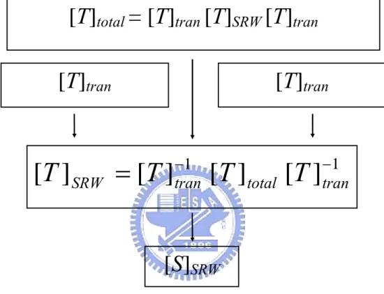
As mentioned above, the integrated synthetic rectangular waveguide (SRW) consists of the SRW and additional waveguide transitions. The effects of mode converters must be de-embedded to obtain the propagation characteristics of the SRW out of two-port scattering analyses or measurements. Herein a single-mode approximation as depicted in Figure 2.6 is presented. The overall measured/theoretical transmission matrix [T]total of the integrated SRW, including two mode converters and
the SRW, was obtained by converting the measured/theoretical S-parameters to T-parameters [45]. The measurement was conducted after the SOLT (short-open-load-through) calibration procedures that had been performed by the HP8510CTM vector network analyzer. The theoretical analysis of the test device, however, was based on HFSSTM full-wave scattering simulation. Next, the [T]tran of
the mode converter was obtained theoretically by HFSSTM based on the single-mode approximation by assuming microstrip, finline, and coplanar waveguide mode of propagation for TE10, TM00, and TM10, respectively. Then the [T]SRW was obtained by
pre- and post-multiplying [T]total by the inverse of [T]tran. Finally, [S]SRW was obtained
by simply converting the corresponding [T]SRW into the [S]SRW.
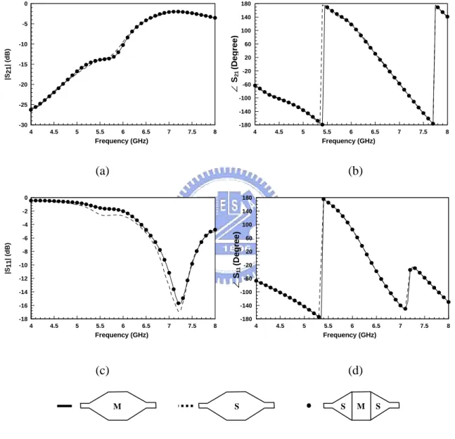
rectangular waveguide with the structural and material constants shown in Fig. 2.1(a) and tapered microstrip mode converter shown in Fig. 2.3 were investigated. Initially, the two-port scattering parameters of the end-to-end integrated rectangular waveguide obtained by measurement and by HFSSTM simulation were compared. Figure 2.7 shows the comparisons. Both data show excellent agreement in magnitude and phase. Then, the measured overall two-port scattering parameters were de-embedded to obtain the complex propagation constant of the conventional rectangular waveguide.
Fig. 2.6 Proposed de-embedding procedures for extracting guiding characteristics of the planar rectangular waveguide.
1
1
]
[
]
[
]
[
]
[
T
SRW
=
T
tran
−
T
total
T
tran
−
[T]
total
= [T]
tran
[T]
SRW
[T]
tran
[S]
SRW
(a) (b)
(c) (d)
Fig. 2.7 Validity check of the proposed de-embedding method for extracting rectangular waveguide parameters: (a) |S21| (b) ∠S21 (c) |S11| (d) ∠S11
10 11 12 13 14 15 16 Frequency (GHz) -25 -20 -15 -10 -5 0 |S21 | (d B ) 10 11 12 13 14 15 16 Frequency (GHz) -180 -140 -100 -60 -20 20 60 100 140 180 ∠ S21 (De g ree ) 10 11 12 13 14 15 16 Frequency (GHz) -30 -25 -20 -15 -10 -5 0 |S11 | (d B ) 10 11 12 13 14 15 16 Frequency (GHz) -180 -140 -100 -60 -20 20 60 100 140 180 ∠ S11 (Degree) M S S M S
Figure 2.8 compares the extracted results with those obtained (2), showing excellent agreement between the two data sets. Therefore we conclude that the single-mode approximation assumed in the de-embedding procedure of Fig. 2.6 is a good approximation for de-embedding the integrated TE10 mode SRW as shown in
Fig. 2.3. In Sections 2.3 and 2.4, the single-mode approximate de-embedding procedure was applied to recover the complex propagation constant of the integrated SRW supporting TE10, TM00, and TM10 modes. The Q-factor of the conventional
rectangular waveguide was also investigated using the basic theory of a rectangular waveguide cavity [45]. The total Q-factor of the conventional rectangular waveguide is the inverse of the summation of 1/Qd and 1/Qc where Qd and Qc are the Q-factors of
the rectangular waveguide with dielectric loss and conductor loss, respectively. The conducting walls, having high conductivity and a thickness of 17 µm, more than five
times the skin depths above the cutoff frequency, were applied to realize a conventional rectangular waveguide, whose Qc is about 9650, between 12 and 20
GHz. However, Qd, which is proportional to the inverse of the tanδ value of the
substrate in the rectangular waveguide, is about 285.7, dominating the power dissipation in the rectangular waveguide. Therefore, the theoretical Q-factor of the conventional rectangular is about 277. However, the measured Q-factor, extracted from the de-embedded propagation constant of the conventional rectangular
waveguide, without the effects of the mode converters, is about 275 between 12 and 20 GHz, indicating close agreement between the measured results and the theoretical predictions.
(a)
(a) (b)
(b)
Fig. 2.8 Comparison of the extracted normalized phase constants of the conventional rectangular waveguide with those obtained by exact equation: (a) phase constant, (b) Q-factor. 11 11.5 12 12.5 13 13.5 14 14.5 15 Frequency (GHz) 100 150 200 250 300 350 400 450 500 Q Theoretical data
Extract from measurement
11 12 13 14 15 16 17 18 19 20 Frequency (GHz) 0 0.2 0.4 0.6 0.8 1 1.2 1.4 1.6 1.8 2 β /k0
Extracted from measurement by de-embedding procedure of Fig. 6 TE10 mode in (2) with µr=1 and εr=3.38
r ε
2.3 TE10 Mode Synthetic Rectangular Waveguide (SRW)
Parallel to obtaining the dispersion diagram of two-dimensional periodical structure made of unit cells shown in Fig. 2.1(d), the master-slave boundaries along the z-direction (longitudinal axis) of Fig. 2.1(c) were applied to solve the complex propagation constant for the SRW. Measured two-port scattering parameters of the integrated TE10 mode SRW shown in Fig. 2.3 were also obtained, then the
de-embedding procedure of Fig. 2.6 was invoked. Figure 2.9 shows measured and theoretical two-port S-parameters of TE10 mode SRW. Both data show excellent
agreement in magnitude and phase.
Fig. 2.10 compares the normalized phase constants (slow-wave factors) obtained by two approaches, showing excellent agreement between the extracted measured data and theoretical results. The cutoff frequency of the TE10 mode SRW was almost
4.10 GHz, which is 0.348 times the cutoff frequency of 11.7 GHz of the conventional waveguide with the same outer dimensions and material constant. The slow-wave factor of the TE10 mode SRW rises quickly to the theoretical limit εr at 4.38 GHz
from the cutoff frequency. Then the slow-wave factor ascends almost linearly to 4.35 at approximately 5.78 GHz. Then it levels off to 4.9 at 6.85 GHz. Meanwhile, the de-embedded Q-factor is about 260, representing only 5.8% degradation in Q-factor as compared to the conventional waveguide although it operates at much higher
frequency. Notably, a conventional rectangular waveguide with the same cutoff frequency using the same dielectric material and thickness as the SRW would have, the lateral dimension of 19.9 mm against 7.0 mm in the SRW design. If the conventional rectangular waveguide has slow-wave factor of εr , approaching the
theoretical limit, immediately produces an estimated area reduction of 6.7 (85%) (at 5.78 GHz) using the particular SRW design. The results clearly demonstrate that the proposed SRW is ideal for miniaturized microwave integrated circuit (MIC) design, which requires a high-Q transmission line.
(a) (b)
(c) (d)
Fig. 2.9 Measured/Simulated two-port S-parameters of TE10 mode synthetic
rectangular waveguide (SRW) parameters (a) |S21| (b) ∠S21 (c) |S11| (d) ∠S11
4 4.5 5 5.5 6 6.5 7 7.5 8 Frequency (GHz) -30 -25 -20 -15 -10 -5 0 |S21 | (d B ) 4 4.5 5 5.5 6 6.5 7 7.5 8 Frequency (GHz) -180 -140 -100 -60 -20 20 60 100 140 180 ∠ S21 (De g ree ) 4 4.5 5 5.5 6 6.5 7 7.5 8 Frequency (GHz) -18 -16 -14 -12 -10 -8 -6 -4 -2 0 |S11 | (d B ) 4 4.5 5 5.5 6 6.5 7 7.5 8 Frequency (GHz) -180 -140 -100 -60 -20 20 60 100 140 180 ∠ S11 (Degree) M S S M S
(a)
(b)
Fig. 2.10 Comparison of the extracted normalized phase constants of the TE10 mode
4 4.5 5 5.5 6 6.5 7 Frequency (GHz) 0 0.5 1 1.5 2 2.5 3 3.5 4 4.5 5 β
/k0 Extracted from measurement by de-embedding
procedure of Fig. 2.6 HFSSTM simulation r ε 4 4.5 5 5.5 6 6.5 7 Frequency (GHz) 100 150 200 250 300 350 400 450 500 Q HFSS TM simulation
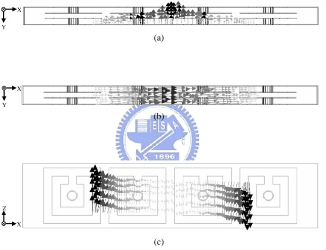
In obtaining the complex propagation constant of the TE10 mode SRW using
HFSSTM simulation, only three field components in the SRW were observed. Figures 2.11 (a), (b) and (c) plot the transverse Ey, transverse Hx, and longitudinal Hz field
components at 6 GHz, respectively. The value Ey and Hx (Fig. 2.11 (a) and Fig. 2.11
(b)) approximately follow the sine distribution and Hz (Fig. 2.11 (c)) the cosine
distribution. Such observations agree well with the field distributions of an ideal TE10
mode waveguide governed by (3), (4), and (5). Thus the results shown in Fig. 2.10 validate the propagation of the TE10 mode in the SRW as shown in Fig. 2.3.
(a)
(b)
(c)
Fig. 2.11 Field distribution of the synthetic TE10 mode rectangular waveguide at 6.0
GHz (a) 2D Ey-field (b) 2D Hx-field (c) 2D Hz-field. X Z X Y X Y
2.4 TM00 and TM10 Mode Synthetic Rectangular Waveguides (SRW)
The making of TM00 and TM10 synthetic rectangular waveguide (SRW) as
illustrated in Figs. 2.4 and 2.5 is beyond our current capability. Thus two theoretical methods were applied to confirm that the TM00 mode and TM10 mode exist in the
proposed SRW. These methods are the de-embedding procedure of Fig. 2.6, and finite element method (FEM) using HFSSTM.
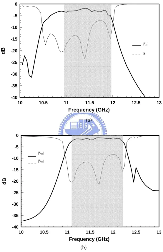
Figures 2.12 (a) and (b) investigate the through characteristics of the back-to-back connected SRW supporting TM00 and TM10 modes, respectively. The
3dB bandwidth is between 10.83 GHz and 11.8 GHz (11.1 GHz and 12.2 GHz) for the integrated TM00 mode (TM10 mode) SRW as shown in Figs. 2.4 and 2.5. Both
transmission regions mentioned above, however, fall into the stopband region of Fig. 2.2, implying that the electromagnetic bandgap (EBG) surfaces behave like magnetic surfaces. Since the transmission losses are relatively high and the bandwidths are relatively narrow, the single-mode approximate de-embedding procedure may not be accurate. Nevertheless, the de-embedding method can generate an estimate of the SRW phase constant.
Figure 2.13 shows the superimposed plots of the normalized phase constants obtained by the de-embedding procedure and HFSSTM simulation, respectively. The
curves with solid and hollow square symbols represent the TM00 mode solutions
obtained by de-embedding and HFSSTM. Data below 10.4 GHz and above 12.3 GHz are not shown for the de-embedding case, since the de-embedding phase constant changed drastically. Between 10.8 GHz and 11.8 GHz, the de-embedding phase constant was about 6.2% lower than that obtained by HFSSTM. It is interesting to notice that the de-embedded phase constant is very close to the HFSSTM data between 10.5 GHz and 10.6 GHz.
(a)
(b)
Fig. 2.12 Scattering analyses of the integrated SRW with various waveguide transitions (a) TM00 mode converter (b) TM10 mode converter.
10 10.5 11 11.5 12 12.5 13 Frequency (GHz) -40 -35 -30 -25 -20 -15 -10 -5 0 dB |S21| |S11| 10 10.5 11 11.5 12 12.5 13 Frequency (GHz) -40 -35 -30 -25 -20 -15 -10 -5 0 dB |S21| |S11|
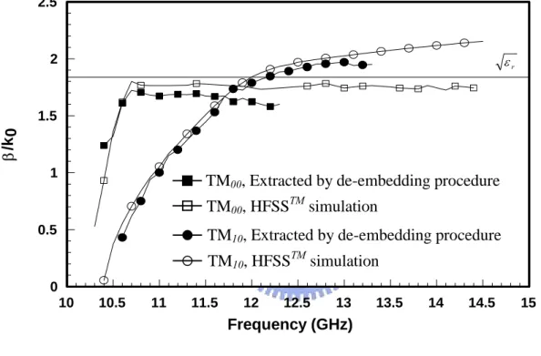
Fig. 2.13 Normalized phase constants of the proposed synthetic TM00 and TM10 mode rectangular waveguides. 10 10.5 11 11.5 12 12.5 13 13.5 14 14.5 15 Frequency (GHz) 0 0.5 1 1.5 2 2.5 β /k0 r ε
TM10, Extracted by de-embedding procedure
TM10, HFSSTM simulation
TM00, Extracted by de-embedding procedure
The slow-wave factor of TM00 mode also rises sharply from the cutoff frequency
near 10.2 GHz and approaches but never exceeds the theoretical limit εr . After
reaching εr at 10.6 GHz, the slow-wave factor flattens and approaches to 14.5 GHz,
beyond which HFSSTM fails to produce stable data. When preparing the TM00 mode
data obtained by HFSSTM upto 14.5 GHz, the modal field distributions were plotted and confirmed to be governed by (8), (9), and (10) for m=0. Figure 2.14 shows the field distribution at 11.0 GHz. Only two field components Ex and Hy, were observed,
and field distributions, which exist only in region between two inner EBG surfaces, were keep uniform along the x-axis. Also, the transverse magnetic field (Hy) shown in
Fig. 2.14 (b) was observed to be perpendicular to the EBG surfaces, and meanwhile the transverse electric field (Ex) as shown in Fig. 2.14 (a) is parallel to the EBG
surfaces. Such observations, which reveal the field distributions of pseudo-TEM mode in the SRW, agree with the ideal TM00 waveguide model shown in Fig. 2.1(b),
(a)
(b)
Fig. 2.14 Field distribution of the synthetic TM00 mode SRW at 11.0 GHz (a) 2D
Ex-field (b) 2D Hy-field. X
Y
X Y
The same investigation and precautions were exercised when plotting the TM10
mode data. The curves with solid and hollow dots represent the TM10 mode solutions
obtained by de-embedding and HFSSTM, respectively. The de-embedding phase constant was about 4.3% lower than that obtained by the HFSSTM data between 10.5 GHz and 10.6 GHz. The slow-wave factor of TM10 mode approaches zero from the
cutoff frequency near 10.4 GHz and exceeds the εrat 11.98 GHz. Then it levels off to
2.2 at 14.5 GHz. Figure 2.15 shows FEM modal field distribution at 11.4 GHz. Only three field components Ex, Hy and Ez were observed. Notably, Figs 2.15 (a) and (b)
reveal that the transverse field components Ex and Hy follow cos(πx a) distributions. In the longitudinal direction, only the Ez component exists, following sin(πx a)
(a)
(b)
(c)
Fig. 2.15 Field distribution of the synthetic TM10 mode rectangular waveguide at 11.4
GHz (a) 2D Ex-field (b) 2D Hy-field (c) 2D Ez-field. X Y X Z X Y
The extracted Q-factors of the TM00 and TM10 mode SRWs were evaluated using
HFSSTM. A series of numerical analyses were performed with different material constant values, including conductivity and loss tangent, to investigate the loss of SRW during the TM00 mode and TM10 mode operations. The Q-factor of the SRW
without conductor loss and dielectric loss is about 664 (673) for TM00 mode (TM10
mode), yielding the intrinsic loss of the SRW. Additionally, Q-factors with either conductor loss or dielectric loss are approximately 548 and 199 for TM00 mode and
555 and 192 for TM10 mode, respectively. The total Q-factors of TM00 mode and
TM10 mode are approximately 187 and 188, respectively. Notably, the total Q-factors
of the TM00 mode and TM10 mode SRW are higher than that of a microstrip line on
the same substrate, indicating that the synthetic integrated TM00 and TM10 mode
waveguides have useful applications in microwave integrated circuit (MIC) and antenna designs.
Table 2.1 Theoretical Q-factor of the TM00 mode SRW at 11.0 GHz.
tanδ
σ
Q-factor
1 0.0
PEC
673
2 0.0035 PEC
192
3 0.0 5.813x10
7555
4 0.0035
5.813x10
7188
Table 2.2 Theoretical Q-factor of the TM10 mode SRW at 11.4 GHz.