國 立 交 通 大 學
光電工程研究所
博 士 論 文
晶片黏貼技術應用於三
晶片黏貼技術應用於三
晶片黏貼技術應用於三
晶片黏貼技術應用於三/
//
/五族化合物
五族化合物
五族化合物
五族化合物
半導體元件效率提升之研究
半導體元件效率提升之研究
半導體元件效率提升之研究
半導體元件效率提升之研究
Study of Efficiency Enhancement for
III/V Compound Semiconductor
Devices by Wafer Bonding Technique
中華民國九十八年十二月
研 究 生 :
指 導 教 授 :
李逸駿
郭浩中教授
盧廷昌教授
晶片黏貼技術應用於三
晶片黏貼技術應用於三
晶片黏貼技術應用於三
晶片黏貼技術應用於三/
//
/五族化合物
五族化合物
五族化合物
五族化合物
半導體元件效率提升之研究
半導體元件效率提升之研究
半導體元件效率提升之研究
半導體元件效率提升之研究
Study of Efficiency Enhancement for
III/V Compound Semiconductor
Devices by Wafer Bonding Technique
研 究 生:李逸駿 Student:Yea-Chen Lee
指導教授:郭浩中 教授 Advisor:Prof. Hao-Chung Kuo
盧廷昌 教授 Prof. Tien-Chang Lu
國
國
國
國 立
立
立
立 交
交
交
交 通
通 大
通
通
大
大
大 學
學
學
學 電機資訊學院
電機資訊學院
電機資訊學院
電機資訊學院
光電工程研究所
光電工程研究所
光電工程研究所
光電工程研究所
博
博
博
博 士
士
士
士 論
論
論
論 文
文
文
文
A dissertation
Submitted to Institute of Electro-Optical Engineering
College of Electrical Engineering and Computer Science
National Chiao Tung University
in partial Fulfillment of the Requirements
for the Degree of
Doctor of Philosophy
In Electro-Optical Engineering
December 2009
晶片黏貼技術應用於三
晶片黏貼技術應用於三
晶片黏貼技術應用於三
晶片黏貼技術應用於三/
//
/五族化合物半導體元件效率提升之研究
五族化合物半導體元件效率提升之研究
五族化合物半導體元件效率提升之研究
五族化合物半導體元件效率提升之研究
學生:李逸駿 指導教授:
國立交通大學光電工程研究所
摘 要
本文主旨是以晶片黏貼的技術製作三五族化合物半導體光電元件之光電特性探 討,利用晶片黏貼技術可以達到異質磊晶的需求,也因此克服了三五族化合物光電元件 因先天晶格匹配的物理限制下無法製作出的結構並達到較好的光電特性。第一部份是探 討將塑膠光纖所用的 650nm 共振腔發光二極體以兩次晶片黏貼之技術,將傳統的砷化鎵 基板以高導熱的矽基板取代,並維持與原先相同結構中的正極朝上與上下布拉格反射鏡 之化合物半導體材料,所製作出元件的電特性與原先結構相近,而元件光特性上具有較 高的光功率輸出、元件對環境溫度與高電流注入影響較低、較低的接面溫度,此外元件 於資料傳輸的測試中可達到 622Mbit/sec。第二部分則是介紹晶片黏貼之技術應用在磷 化鋁銦鎵的發光二極體元件,前半部份是利用膠合黏貼與溼蝕刻的技術,將傳統吸光且 導熱差的砷化鎵基板以高透光的藍寶石基板取代,並以高溫濕蝕刻方式將藍寶石基板側 壁做非等相性蝕刻,此具有基板側壁導角的元件將可以大幅增加光淬取效率,另外考量 藍寶石基板的散熱特性較差,元件亦製作出覆晶型式且具有側壁導角之發光二極體元 件,由於發光區接近矽基板且具有很厚的窗口層於元件表面,因此覆晶型式結構的發光 效率與元件特性相較於前者可以大幅提升;而後半段則是利用金屬黏貼技術將砷化鎵基 板以矽基板取代,藉此能提高元件在高溫或高電流注入之效率,此外為了提升光淬取效 率在元件的表面製作出結構化,其中包含了微米尺寸之碗狀陣列結構,以及在微米碗狀 結構中以奈米球塗佈與乾蝕刻方式製作出奈米尺寸之柱狀結構,這相較於傳統表面平整 之元件可增加兩倍光淬取效率。第三部分則是介紹將金屬黏貼技術應用在氮化鎵材料之 藍綠光發光二極體元件,搭配雷射剝離技術將傳統藍寶石基板以高導熱矽基板取代,首 先晶片黏貼前以雷射挖取溝槽將可提升雷射剝離之良率;將優化的鋁銀合金做為歐姆接 觸材料與反射層的技術運用結構中,鋁銀合金不但具有高反射率且有較好高溫穩定性, 另外為了解決氮表面歐姆接觸不易,高濃度摻雜與清洗方式將可大幅降低接觸電阻,此 外優化後氫氧化鉀溶液將可以大幅提升光淬取效率,最後元件相較於傳統藍寶石基板之 氮化物發光二極體具有較佳的光電特性、較低的熱阻抗與穩定的可靠度。郭浩中 教授
盧廷昌 教授
Study of Efficiency Enhancement for III/V Compound Semiconductor
Devices by Wafer Bonding Technique
Student: Yea-Chen Lee Advisor:
Institute of Electro-Optical Engineering, National Chiao Tung University
Abstract
This dissertation is study of wafer bonding technique applied for III-V compound semiconductor optoelectronic devices. The wafer bonding technique overcomes hetero-epitaxy growth and achieving better electrical and optical performances which are restricted by physical barrier of lattice match requirement. Firstly, the conventional 650nm RCLEDs for plastic optical fiber with GaAs substrate is replaced with a high thermal conductivity Si substrate by glue bonding and metal bonding technique. This MBRCLEDs is maintained p-side up and DBRs materials structure and without sacrificing electrical performances. The MBRCLEDs has higher output power, high temperature insensitivity, less decay in high current injection, lower junction temperature as compared with conventional RCLEDs. Furthermore, the MBRCLEDs have superior reliability and achieve 622Mbit/ sec. Second, the glue bonding technique is applied to AlGaInP-based LEDs. The conventional GaAs substrate, having inherent drawbacks of poor thermal conductivity and absorbed, is replaced with a transparent sapphire substrate. The sapphire substrate sidewall has geometric shaping by using high temperature chemical etchant. This geometric sapphire shaping LEDs provide superior light extraction efficiency as compared to without one. In order to improve thermal issue in sapphire substrate, the flip-chip structure is applied for improving. The flip-chip AlGaInP-based LEDs have thick window layer of sapphire, which has geometric sidewall shaping, p-side layer close to Si submount for thermal dispersion. This flip-chip structure provides an excellent light extraction efficiency and stable reliability. Furthermore, the metal bonding technique is implemented in AlGaInP-based LEDs, and the GaAs substrate is replaced with Si substrate. The metal bonding LEDs have textured surface for increasing light extraction efficiency. Several textures of micro scale bowls array and nano scale rods added in micro bowls are implemented by anisotropic chemical etching and nano-spheres spin-coating with dry-etching. Comparing to conventional plane surface, the nano-rods added in micro-bowls surface LEDs has two magnitudes output power due to less total internal reflection effect. Finally, the vertical thin film GaN-based LEDs are fabricated by metal bonding and laser-lift-off technique. In order to release internal stress and improve yield after laser lift-off process, a laser cut trench before metal bonding process is used. The optimized Al an Ag composition to form AlAg alloy for p-ohmic contact and high reflector application is applied. The AlAg alloy provides not only high reflectivity but also high thermal stable property. In order to solve n-ohmic contact at N-face n-GaN layer, higher doped n-GaN layer and chemical cleaning at N-face are also implemented. The optimized KOH chemical etchant for surface roughing is applied for enhancing light extraction efficiency. Comparing to conventional sapphire-based GaN-LEDs, the vertical thin film GaN-based LEDs has higher output power under equal current density, lower forward voltage, less wavelength shift under high current injection and high ambient temperature, lower thermal impendence, and higher
Prof. Hao-Chung Kuo
Prof.
Tien-Chang Lu
誌謝
誌謝
誌謝
誌謝
經過四年半的博士班生涯,如今能順利取得學位,首先要感謝指導教授郭浩中與盧 廷昌教授,經過兩位指導教授耐心的指導與細心教誨下,讓我在這段求學過程中能更佳 順利學習與成長,並增加了相關專業知識領域廣度與深度,尤其是郭浩中教授無時無刻 的督促與從旁協助,提供相關研究方向與意見,使我在這四年半獲益良多,因此很感謝 郭浩中教授對我的提攜。 再來最要感謝的就是碩士班時的學弟兼博士班的同窗李佳恩同學,四年半前一起進 入實驗室,四年半後也一起順利的畢業,因我們在實驗室的時間不長,因此這四年半都 是相依為命,為了完成畢業的夢想,在實驗上相互幫忙協助與分享結果,資訊互通有無; 然而,其間的許多的糊塗事與小插曲也一起渡過與承擔,但其中一些插曲實在仍需再次 感謝郭浩中教授的鼎力相助,方能讓我們順利完成學業。 接著要感謝的就是我工作上的貴人,首先最要感謝的是現任禧通科技技術協理邱舒 偉博士,感謝邱舒偉博士在我國聯光電服國防役四年與帶我離開後兩年時一路的提攜, 從邱舒偉博士身上學到許多專業知識與對事情的執著,也建立我日後對工作上嚴謹的態 度;接著要感謝現任聯勝光電總經理張智松博士,感謝張智松博士在國聯光電研發部時 期的提攜,並體諒求學過程中所造成的工作困擾;另外感謝現任聯勝光電研發協理顏良 吉準博士,感謝顏協理在這兩年中教導我許多過去從未接觸的事物,從顏協理身上獲取 無數寶貴的經驗與知識;另外,也感謝目前我工作上的伙伴昌翰、煒竣、逸凡、書帆、 琮耀與毅君,感謝你們幫我整理資料、製作樣品與收集相關實驗結果,使我論文資料撰 寫能更完整。雖不常在實驗室,但仍感謝許多博士班學弟們的協助,其中包含清華、柏 孝、士偉、明華與小賴,感謝你們為我與佳恩所做的一切,也再次感謝學長黃泓文博士 於我博士求學生涯最後實質上的協助。 最後,我要把感謝留給我的家人,感謝爸爸、媽媽在我求學過程中做最大努力與無 怨無悔的付出,雖然一路風風雨雨、跌跌撞撞,曾經讓您們很失望,但我現今的成就完 全歸功於您們全力支持與付出所換來的,感謝您們與逸文對我所付出的一切;最終,感 謝未婚妻伊晴六年來的陪伴與照顧,我們將一起努力完成我們未來美好的人生,感謝妳 的體諒與付出。也再次感謝曾經幫助過我的人。 逸駿逸駿逸駿逸駿 于 于 于 于
交大光電
交大光電
交大光電
交大光電
2009.12.16Contents
Abstract (in Chinese)………...i
Abstract (in English)………...ii
Acknowledgement……….iii
Contents………...iv
List of Figures………...….vi
Chapter 1 Introduction
...11.1 Overview…....……….………..1
1.2 Outline of This Dissertation…………..………....2
References
Chapter 2 High-Performance AlGaInP-Based Resonant-Cavity Light-
Emitting Diodes in Wafer Bonding Technology
…….….…...…….72.1 Introduction……….………..7
2.2 The RCLEDs Principle Operation and Epi-Structure Design………...….…...9
2.3 Fabrication Processes of 650 nm AlGaInP-based RCLEDs………...…12
2.3.1 Standard 650 nm RCLEDs Processes with GaAs Substrate………..…… 12
2.3.2 High Performances 650 nm RCLEDs Processes with Si Substrate in Twice Wafer Bonding Technique ……….…………...13
2.4 Performances of 650 nm AlGaInP-based RCLEDs and MBRCLEDs…..….…15
2.5 Summary………...……..20
References
Chapter 3 Light Extraction Enhancement of AlGaInP-Based Light-
Emitting Diodes in Wafer Bonding Technique
………..473.2.1 AlGaInP-Based LEDs with a Geometric Sapphire Substrate……….……49 3.2.2 AlGaInP-Based Flip-Chip LEDs with a Thick Geometric Sapphire
Substrate Window layer……….……….52 3.3 Enhancing Light Extraction Efficiency of Surface Textured AlGaInP-Based
LEDs in Metal Bonding…....……….…….……57 3.4 Summary………...61
References
Chapter 4 High Performances of InGaN/ GaN Light-Emitting Diodes in
Metal Bonding Technique
………89 4.1 Introduction………..………...89 4.2 Semi-Vertical InGaN/ GaN Light-Emitting Diodes with Single Electrode-PadFabricated on Sapphire Substrate………..………91 4.2.1 Introduction……….91 4.2.2 Fabrication of Single Electrode Pad InGaN/ GaN LEDs (SEP-LEDs)…..92 4.2.3 Characteristic of Single Electrode Pad InGaN/ GaN LEDs (SEP-LEDs)..93 4.3 Vertical InGaN/ GaN Light-Emitting Diodes by Metal Bonding Techniques....96 4.3.1 Introduction………...….…….96 4.3.2 Fabrication of Vertical Thin Film InGaN/ GaN LEDs (VTF-LEDs)……..96 4.3.3 Characteristic of Vertical Tthin Film InGaN/ GaN LEDs (VTF-LEDs)...99 4.4 Summary…..……….…112
References
Chapter 5 Conclusion and Future Works
…...147List of Figures
Chapter 1
Figure 2.1 Attenuation of a PMMA step-index plastic optical fiber...25
Figure 2.2 Intensity of the optical mode at the top mirror for an m=1 cavity. While the reflectivity of the bottom DBRs was r22=1, the reflectivity r1 of the top DBRs was varied………...………....………26
Figure 2.3 Intensity of the optical mode at the top mirror for an m=1 cavity for various detuning d. The reflectivity of the top DBRs was r12=0.6 and the bottom DBRs was r22=1………...….……….27
Figure 2.4 The 650nm AlGaInP-based RCLEDs epi-structure……...….….………28
Figure 2.5 Schematic fabrication processes of RCLEDs devices (1)~(9)……….29
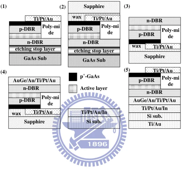
Figure 2.6 Schematic diagram of MBRCLEDs fabrication (1)~(5) ……….31
Figure 2.7 The OM figures of three different light emission window sizes of 84, 60 and 40 µm………...…...…….…...…...………...……32
Figure 2.8 The typical light intensity-current-voltage (L-I-V) characteristics of 84, 60, and 40 µm aperture size RCLEDs...33
Figure 2.9 The wall-plug efficiency and output power characteristics of 84 µm devices with epoxy encapsulated...34
Figure 2.10 The output power variation versus detuning wavelength...35
Figure 2.11 The coupling efficiency versus wide driving current into 0.5NA POF...36
Figure 2.12 The cut-off frequency -3dB of these three different devices operated at 20 mA..37
Figure 2.13 The eye diagram of 40 µm RCLEDs could achieve 622 Mbit/s...38
Figure 2.14 The eye diagram for the transceiver using RCLEDs devices with single QW transmitting 500 Mbit/s data rate through graded-index POF over 50 m...39
Figure 2.16 The typical intensity-current (L-I) characteristics of the MBRCLEDs and the RCLEDs versus temperature variations...41
Figure 2.17 The wall plug efficiency as a function of injection current for the MBRCLEDs and the RCLEDs at RT...42
Figure 2.18 Junction temperature increase and forward voltageas a function of the injection current for MBRCLEDs and conventional RCLEDs at room temperature...43
Figure 2.19 The far-field patterns of the MBRCLEDs devices under 20 mA current injection versus ambiance temperature of (1) 25°C, and (2) 85°C...44
Figure 2.20 Reliability results of the MBRCLEDs and the RCLEDs under a condition of 85°C and 20 mA driving current for life test...45
Figure 2.21 (1) 25 °C and (2) 80 °C eye diagram of the MBRCLEDs under 20 mA driving current. The scale in the figure is 2.5 ns/ div...46
Chapter 3
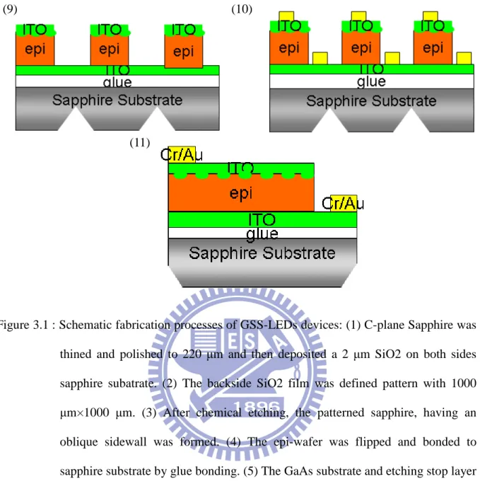
Figure 3.1 Schematic fabrication processes of GSS-LEDs devices (1)~(11)...66
Figure 3.2 (1) Schematic diagram of the GSS-LEDs structure with surface textured and sandwich transparent conductive ITO layer. (2) Illustrated that the different extracted light path of the GSS-LEDs and the conventional GB-LEDs...68
Figure 3.3 Scanning electron micrographs of sapphire shaping structure (1) cross-section and (2) top views. (3) Formation of the V-shape groove with etching time...69
Figure 3.4 SEM images of (1) (2) schematic diagram of the AlGaInP-based GSS-LEDs structure. (3) (4) illustrated the wafer surface with a nano-roughed texture on the thick n-AlGaInP surface layer via natural cluster metal nano-mask and chemical etching processes...70
Figure 3.5 A tilted cross-section photomicrographs view of (1) GB-LEDs and (2)
GSS-LEDs chip under a forward current 70mA injection...71
Figure 3.6 The corresponding luminous intensity-current-voltage (L-I-V) characteristics of the conventional GB-LEDs and the novel GSS-LEDs...72
Figure 3.7 Beam patterns of the GB-LEDs and GSS-LEDs under 70 mA injection...73
Figure 3.8 Fabrication flowcharts of the GSS-FCLEDs...74
Figure 3.9 (1) Schematic diagram of the AlGaInP GSSFC-LEDs structure. (2) SEM figures of the top view of geometric sapphire shaping substrate profile and (3) Cross section profile. (4) Described with the possible photons paths inside the
structure of the GSSFC-LEDs and the CFC-LEDs...75
Figure 3.10 (1) Ni nano-cluster hard mask after RTA treatment. (2) Epi-wafer surface with random rough texture after ICP dry-etching process...76
Figure 3.11 (a) (b) The wall-plug efficiency of the GSSFC-LEDs and CFC-LEDs. (c) ~ (e) The L-I characteristics of the GSSFC-LEDs, CFC-LEDs and CGB-LEDs...77
Figure 3.12 Reliability results of the CGB-LEDs and CFC-LEDs under 350-mA current injection in room temperature ambience...78
Figure 3.13 The light output pattern of the CFC-LEDs and GSSFC-LEDs...79
Figure 3.14 The schematic diagram and simulated ray-tracing images of (1) CFC-LEDs and (2) GSSFC-LEDs...80
Figure 3.15 The simulated candela maps images of (1) CFC-LEDs and (2) GSSFC-LEDs...81
Figure 3.16 Schematic diagrams of the metal bonding AlGaInP-based LEDs (1) The LED-I device structure has a plane surface. (2) The LED-II device has micro-bowls array texture on surface and the LED-III device is added nano-rods texture in moicro-bowls...82
Figure 3.17 Schematic diagrams of (1) Each hard mask dimension and distance of photo resistance dot is 3 µm. (2) After anisotropic wet etching, the 5 µm wide micro-bowls were formed on surface. (3) The silica nano-particles were spin-coated on the wafer surface which has bowl-shaped textured. (4) After dry-etching process, the nano- rods were formed on surface...83
Figure 3.18 SEM figures of (1) The LED-II chip profile. (2) ~ (4) The LED-II surface were covered with micro-bowls...84
Figure 3.19 SEM figures of (1) The silica nano-particles were spin-coated on wafer surface and sphere diameter is 120 nm. (2) ~ (4) The nano-rods were formed on surface
Figure 3.20 The corresponding luminous intensity-current-voltage (L-I-V) characteristics of the LED-I, LED-II, and LED-III...86
Figure 3.21 The LED-I, LED-II, and LED-III characteristic of the wall-plug efficiency and output power versus current...87
Figure 3.22 The beam patterns of the LED-I, LED-II, and LED-III under 20 mA current injection...88
Chapter 4
Figure 4.1 (a) Schematic diagram of SEVENS LEDs structure (b) Microscope image of chip, and (c) Electroluminescence photograph image under 20-mA current for SEVENS-LED fabricated by sapphire wet etching...119
Figure 4.2 Schematic diagrams of (a) The expanded chips were flipped and embedded in PR (b) The structure of single electrode pad GaN-based LEDs (SEP-LEDs) fabricated on sapphire substrate...120
Figure 4.3 Scanning electron microscope (SEM) images of (a) Chip profile (b) Detail description (c) Top-view of p-GaN surface roughness (d) Surface textured of ITO layer by photolithography and chemical wet-etching...121
Figure 4.4 (a) Typical current versus voltage (I-V) characteristics of SEP-LEDs and CL-LEDs (b) Wall-plug efficiency and output power in relation to injection current of SEP-LEDs and CL-LEDs...122
Figure 4.5 Optical and EL microscope images of (a) SEP-LEDs and (b) CL-LEDs...123
Figure 4.6 I-V characteristics as a function of a reverse pulse voltage in a machine-model ESD driving for (a) SEP-LEDs (b) CL-LEDs...124
Figure 4.7 Schematic fabrication processes of VTF-LEDs (a)~(n)...125
Figure 4.8 (a) The chip profile of VTF-LEDs and the chip size is 1200 µm×1200 µm. (b) The current spreading performance in VTF-LEDs metal mesh line design. (c) The tilted cross-section EL image of green and blue VTF-LEDs...128
Figure 4.10 The SEM figures of Ni/ Ag metal on p-GaN surface after. (a) as-deposition (b) 400°C (c) 500°C (d) 600°C (d) 700°C different thermal treatment...130
Figure 4.11 The O&R metal reflectance of various compositions under different alloy
temperature...131
Figure 4.12 XPS atomic depth profile of Ni/ Ag and Ni/ Al/ Ag composition before and after thermal treatment at 500°C in ambient air...132
Figure 4.13 Schematic diagram of (a) Al/ Ag was deposited on p-GaN. (b) After annealing, an AlAg eutectic layer was formed. (c) The AlAg eutectic phase diagram...133
Figure 4.14 The L-I characteristic of O&R layer as-deposition and after annealing...134
Figure 4.15 (a) The I-V curve, and (b) Reflectively of various aluminum thicknesses after 500ºC thermal annealing...135
Figure 4.16 Schematic illustration of GaN wurtzite crystal structure exhibiting the polarity along the c-axis...136
Figure 4.17 The I-V curves of Pd/ Ti/ Al and Cr/ Au deposited on N-face surface of n-GaN, which has (a) 5×1018 cm-3 carrier concentrations and (b) 1×1019 cm-3 carrier concentrations...137
Figure 4.18 The specific contact resistance of (a) Ga-face and N-face under various alloy temperature and (b) Different chemical treatment of Ga-face and N-face under various alloy time...138
Figure 4.19 The (a) I-V and (b) L-I characteristic of VTF-LEDs and CL-LEDs...139
Figure 4.20 The current density versus lumen intensity of VTF-LEDs and CL-LEDs...140
Figure 4.21 (a) The spectrum variation of of VTF-LEDs and CL-LEDs under different
ambience. (b) The spectrum variation of VTF-LEDs under different current....141
Figure 4.22 SEM images of the N-face surface morphology after immerging in 85ºC 1M KOH chemical for (a) (b) 5min, (c) (d) 6min, (e) (f) 7min, and (g) (h) 8min....142
Figure 4.23 SEM images of the N-face GaN etching morphology using (a) (b) 65ºC and (c) (d) 95ºC 2M KOH for 5min...143
Figure 4.25 The VTF-LEDs and CL-LEDs were operated at 0.1 mA and measured forward voltage under varied ambient temperature (20°C to 150°C)...145
Figure 4.26 The VTF-LEDs reliability performance of (a) forward voltage variation and (b) power variation under 350 mA and room temperature for 1800 hours...146
Chapter 5
Figure 5.1 Schematic diagram GaN-based VCSELs structure of (a) vertical current injection and (b) optical pumping configuration fabricated by using wafer
CHAPTER 1
Introduction
1.1 Overview
“Wafer bonding” technique generally refers to the process that two mirror-polished wafer
adhere to each other. Wafer bonding is alternatively knows as “direct bonding” and “fusion
bonding”. The wafer bonding technique can combine with any two (ore more) different
semiconductor materials on a substrate or film after bonded wafers surface proper polishing
and chemical treatment. The wafer bonding technique is independent of whether the bonded
materials are crystal or noncrystal, the lattice orientation and parameter, the surface doping
type and profile, and the bonded materials thickness. In other words, the wafer bonding
technique could solve any materials integrated issue in semiconductor process. Recent years,
many groups have been widely investigated wafer bonding technique, especially the III-V
compound semiconductors optoelectronic devices are integrated on silicon. The integration of
III-V optoelectronic devices on silicon integrated circuits could be formed the optoelectronic
integrated circuits (OEICs) [1]-[3]. Te OEICs technique is highly desirable for optical fiber
data communications and optical interconnects. The III-V compound semiconductors are
main materials for optoelectronic devices, such as optical amplification, laser diodes (LDs),
vertical-cavity surface-emitting laser (VCSEL), and light-emitting diodes (LEDs). However,
the optical devices of III-V compound semiconductor are grown on III-V materials substrate
due to the physical limitation of epitaxy lattice match. Therefore, the integration of III-V
optoelectronic devices with silicon for OEICs application could be realized by wafer bonding
technique. Wafer bonding technique solves a problem of dislocations caused by the epitaxy
InP/GaAs [6] wafer bonding have been demonstrated for laser diodes, light-emitting diodes,
detectors, and waveguides. Therefore, wafer bonding is an alternative technique for achieving
the purpose of growing epi-layer transferred to another substrate or film. By wafer bonding
technique, it is accomplished hetero-epitaxial between lattice mismatch materials and without
sacrificing devices performances. Therefore, the III-V compound semiconductor
optoelectronic devices via this technique are more flexible and valuable for applications.
1.2 Outline of This Dissertation
In this dissertation, the wafer bonding technique is used for enhancing efficiency of III-V
compound semiconductor. All of investigations are based on wafer bonding technique,
including metal bonding, glue bonding, and twice bonding. The device conventional substrate
was removed and replaced with a new substrate, such as a high thermal conductively silicon
substrate or a transparent sapphire substrate. After exchanging the conventional substrate, the
III-V devices could achieve higher efficiency and characteristic, such as light extraction
efficiency enhancement, high temperature insensibility and stability, suitable for high current
operating, and stable performances in high temperature ambience.
In chapter 2, the high performances 650 nm resonant-cavity light-emitting diodes
(RCLEDs) were demonstrated via high quality epitaxy and excellent chip process. The
RCLEDs were designed with different light-output aperture sizes 84, 60, and 40 µm, for
different applications of plastic optical fibers. In order to solve the RCLEDs performance in
high temperature operation, the metal bonding RCLEDs (MBRCLEDs) with high
performances, high temperature insensitively, and high reliability have been successfully
fabricated on Si substrates by twice wafer bonding techniques. By wafer bonding technique,
the RCLEDs, growing on conventional GaAs substrate, were replaced with a high thermal
changed GaAs substrate. Therefore, the MBRCLEDs maintained original RCLEDs
performances and improve devices characteristic under high temperature ambiance especially.
The junction temperature variations of the MBRCLEDs were also relatively smaller as
compared with the RCLEDs. Furthermore, the stable beam profile, high reliability over 1000
hours and clearly eye diagram in high temperature operation. These excellent performances of
the MBRCLEDs devices should be suitable for high temperature ambiance, high current
injection and high data communication applications.
In chapter 3, several methods to enhance AlGaInP LEDs performances were
demonstrated. The AlGaInP LEDs performances enhancement key points in this study is to
replace the absorbing GaAs substrate with a transparent sapphire substrate or high thermal
conductively silicon substrate, and then fabricates surface textured for reducing total internal
reflection effect. The LEDs efficiency enhancements are based on wafer bonding techniques
of glue bonding and metal bonding process, and the surface roughness, geometric structure
and flip-chip techniques were also applied for enhancing AlGaInP LEDs performances. The
AlGaInP LEDs with a transparent sapphire substrate were fabricated by glue bonding method.
This transparent sapphire substrate is a geometric shaping sidewall (GSS-LEDs) structure by
chemical wet etching processes. The GSS-LEDs surface has a nano-roughened texture by
natural mask and chemical wet etching processes in order to improve light extraction
efficiency. It was demonstrated that the GSS-LEDs structure could not only reduce the TIR
effect but increase more probabilities of output light escaping from the transparent substrate
due to the oblique sidewall structure. The GSS-LEDs are still not suitable for high current
injection or high temperature ambience operating especially in short wavelength of AlGaInP
system material. For this reason, a novel flip-chip AlGaInP-LEDs structure which has a thick
output power, longer reliability and higher wall-plug efficiency as compared with GSS-LEDs,
conventional flip-chip LEDs (CFC-LEDs), and conventional glue bonding LEDs (GB-LEDs).
Finally, the AlGaInP epi-layers were bonded to a high thermal conductive Si substrate via
metal bonding technique due to the sapphire is not a perfect substrate in devices, and achieved
excellent light extraction efficiency using micro- and nano-scale surface textured technique.
This structure, having micro-bowls and nano-rods texture on surface has the highest output
power as compared with micro-bowls only and plane surface devices.
In chapter 4, the InGaN/ GaN LEDs efficiency was enhanced by metal bonding, laser
lift-off, and surface roughness technique. The conventional InGaN/ GaN LEDs with
non-conductive and poor thermal conductivity property of sapphire substrate were replaced
with Si substrate. Firstly, a novel and simple structure of single electrode pad (SEP-LEDs) in
GaN-based LEDs are demonstrated. The concept was come from laser diode process of face
coating. The ITO film was deposited on SEP-LEDs sidewall, and then a conductive current
path was formed from chip sidewall to sapphire backside by ITO film. The SEP-LEDs has
high performances than conventional lateral LEDs (CL-LEDs) although both substrates are
sapphire. It is attributed that SEP-LEDs has more light output area and uniform current
spreading properties. However, the SEP-LEDs structure can not be applied in future LED
applications of high output power, high efficiency under higher current density, temperature
insensitivity operating, and high reliability property after all. For this reason, the InGaN/ GaN
vertical thin film LEDs (VTF-LEDs) structure is an important tread toward future LED
lighting application. Many techniques and experiments are implanted in VTF-LEDs for
improving VTF-LEDs performances and enhancing efficiency, such as high thermal stable
Al-Ag alloy metal for reflector and p-ohmic contact, laser double cut before LLO process,
proper chemical treatment and heavily doped in n-GaN layer for solving N-face surface of
is demonstrated that the VTF-LEDs with lower forward voltage, uniform current spreading,
high efficiency under the same current density, less wavelength variation in high current and
high temperature ambience operating, higher maximum junction, and excellent thermal
REFERENCE
[1] H. Wada; T. Takamori; and T. Kamijoh, “Room-temperature photo-pumped operation of 1.58-µm vertical-cavity lasers fabricated on Si substrates using wafer bonding”, IEEE
Photon. Technol. Lett., vol. 8, pp. 1426–1428, Nov. 1996.
[2] H. Wada; T. Kamijoh, “Room-temperature CW operation of InGaAsP lasers on Si fabricated by wafer bonding”, IEEE Photon. Technol. Lett., vol. 8, pp. 173–175, Feb.
1996.
[3] Long Chen, Po Dong, and Michal Lipson, “High performance germanium photodetectors integrated on submicron silicon waveguides by low temperature wafer bonding”, Optics
Express, Vol. 16, Issue 15, pp. 11513-11518, 2008.
[4] A. Georgakilas , M. Alexe , G. Deligeorgis , D. Cengher , M. Androulidaki , S. Gallis , Z. Hatzopoulos and G. Halkias “III-V material and device aspects for the monolithic
integration of GaAs devices on Si using GaAs/Si low temperature wafer bonding,” CAS
2001 Proc. Piscataway, NJ: IEEE, pp. 239, 2001.
[5] Q.-Y. Tong, Q. Gan, G. Hudson, G. Fountain, and P. Enquist, “Low temperature InP/Si wafer bonding”, Appl. Phys. Lett. 84, 732 (2004).
[6] Hui Huang, Xiaomin Ren, Xinyan Wang, Qi Wang, and Yongqing Huang, “Low-temperature InP/GaAs wafer bonding using sulfide-treated surface”, Appl. Phys.
CHAPTER 2
High-Performance AlGaInP-Based Resonant-Cavity Light-Emitting Diodes
in Wafer Bonding Technology
2.1 Introduction
In recent years, low-cost and short-distance-network optical devices based on the
polymethyl methacrylate (PMMA) plastic optical fiber (POF) have been widely used for data
communication, medium, automotive industry, and industrial sensors etc... The new
development of these optical devices were focused on such factors as high power, high
efficiency, high modulation speed, high coupling efficiency, reliability, low-cost fabrication,
and high temperature insensitivity. On the basis of these requirements, the AlGaInP-based red
650 nm resonant-cavity light-emitting diodes (RCLEDs), according to these requirements,
have been developed. A typical RCLED structure consists of an active layer for light emitting
placed in a Fabry-Perot (F-P) resonator [1]. The F-P mirrors used are typically
quarter-wavelength (λ/4) thickness semiconductors, dielectric distributed Bragg reflectors
(DBRs) [2], or higher reflective metal films [3]. The RCLEDs structures are different from the
conventional LEDs in some properties, such as optical profiles of directionality, narrower
spectral bandwidth, higher quantum efficiency, higher output intensity, and suitable for optical
communication of light sources [4]-[7]. The RCLEDs structure is similar to that of
vertical-cavity surface-emitting lasers (VCSELs). Both of them have a high reflectivity
(>98%) n-DBR as a function of bottom reflector, but the amount of top p-DBR pairs in
RCLEDs structure is less than that in VCSELs. Actually, red visible VCSELs could not be
operated in high-temperature environments such as in automobile parts or
temperature sensitivity could be controlled by modifying the detuning cavity wavelength [9].
The detuning wavelength (λdetuning) means that the different wavelengths of the F-P resonator
and the quantum well:
λdetuning = λFP – λQW, (2-1)
where λFP and λQW are the wavelengths of the F-P resonator and quantum well, respectively.
The most important function of optimum detuning structure wavelength is that the devices
temperature insensitively. In short-distance optical communication applications, POF offers
several advantages over glass fiber such as low cost, higher number aperture (NA) for high
coupling efficiency, decreasing fiber weight, visible light source for safety, and fiber
flexibility. In order to meet these demands for high-performance POF communication,
selected a light source to achieve high efficiency, reliability, suitable modulation bandwidth,
operating-temperature range extensity, and higher coupling efficiency is very important.
Therefore, the visible red 650 nm RCLEDs is more ideal light source than conventional LEDs
and VCSELs for the standard step-index polymethyl methacrylate (PMMA) based fibers due
to the low-loss band (0.2 dB/m) at 650 nm [10]. The attenuation in plastic fiber is shown in
figure 2.1. The preferred communication window of plastic fibers is at 650 nm, where the loss
is of the order of 0.1-0.2dB per meter. At even shorter wavelengths, the attenuation in plastic
fibers decreases.
In this chapter, we will discuss the high performance of 650 nm RCLEDs devices under
special epi-structure and chip process firstly. And then we will introduce the high efficiency
and temperature insensitive RCLEDs which were produced using twice wafer bonding
technique. Finally, we will present all performances not only electrical and optical properties
2.2 The RCLEDs Principle Operation and Epi-Structure Design
The epitaxial structure of 650nm RCLEDs is very similar to red VCSELs. Both of them
have a high reflective mirror in bottom, which the reflectivity is approximately 100%.
Nevertheless, RCLEDs has lower number of periods top DBRs, which normally is between
four and eight periods. In the spontaneous emission of RCLEDs is no longer isotropic due to
the Fabry-Perot resonances certain wavelengths are allowed for certain directions only. A
detailed theoretical analysis of properties of RCLEDs was shown as reference of Benisty et al.
[11]. Here the points will be focused on the simple contentions and shows the relationship
between the wavelength detuning and the enhancement of light extraction efficiency.
The light source centered between a reflectivity r1 of top DBRs for electrical field and a
bottom DBRs with a reflectivity r2 can find a formula as following for the electrical field at
the top DBRs by calculating the path and phase differences, and summing up for multiple
paths in Fabry-Perot cavity:
− + − = φ −φ φφ i i i i r e r r e r e )e r ( (θ E 2 1 2 / 2 2 / 1 1 1 1 ) , (2-2)
where θ is the angle between the normal top DBRs vector and the propagation direction of the
output light wave. The phase factor φ is given by:
θ λ λ π φ 2 rescos m = , (2-3)
where λres is the resonance wavelength of the cavity and m is the order of the cavity. The light
extraction efficiency ηescape could be estimated by integrating the power emitted into the
escape cone divided by overall power emitted into all direction:
' ' sin ) ' ( ) ' ( ' ' sin ) ' ( ) ' ( * 1 0 1 * 1 0 1 θ θ θ θ θ θ θ θ η θ π θ θ θ θ d E E d E E r r r c r escape ⋅ ⋅ =
∫
∫
= = = = , (2-4)which has an m=1 cavity and varied reflectivity was shown in figure 2.2. The useful mode for
light extraction, since the output light that propagates in directions with θ<θc could be emitted
through the top DBRs. In figure 2.2, we can find that the mode is concentrated more and more
inside the light escape core with increasing the reflectivity of the top DBRs. Depending on the
order of the cavity this leads to an optimal reflectivity of the top DBRs under the reflectivity
of the bottom DBRs should be approximately to 100%. The light extraction efficiency could
be further fine tuned using a detuning d between the quantum well and the normal
Fabry-Perot resonance: res qw res d
λ
λ
λ
− = , (2-5)This equation is illustrated and shown in figure 2.3. In equation 2-4, the Fabry-Perot
resonances have to increase a factor of sin θ, thus it could be enhanced more output light to
emit in solid angle element. It is useful to have the peak emission wavelength of the quantum
wells tuned to be in resonance with the cavity at an oblique angle within the escape cone, and
an optimum for the detuning is around d=4% [12]. The AlGaInP RCLEDs design should be
comprised a higher reflectivity bottom DBRs and the top DBRs with a reflectivity (r12)
around 0.3 to 0.8. In order to fit the extraction into the Fabry-Perot extraction mode and inside
the escape cone, the spectrum of quantum well emission should be small enough. The
effective cavity length consisting of an active layer and the penetration depths into the DBRs
should be as small as possible demanding to use the maximum value of reflective index
contrast for reducing the absorption in the DBRs.
An important parameter in view of the POF communication system application is the
RCLED modulation bandwidth. Two major factors can influence the modulation bandwidth:
the non-radiative recombination lifetime and carrier density in the active region. The small
+ + = − qV BI f nrl nrl dB 2 3 2 1 2 1 2 1 τ τ π , (2-6)
where q is the primary charge and B is the band-to-band recombination rate. Usually the
carrier loss though leakage current does not taken into consideration but for the red
wavelength range the carrier leakage significantly affects the carrier lifetime and the current
density. Since the leakage carrier are finally lost by non-radiative recombination outside the
active region and it is difficult to discriminate the leakage lifetime, an overall non-radiative
recombination lifetime (
τ
nrl) including the leakage lifetime should be considered.In this study, the epitaxy structure were grown on a 3-inch GaAs substrate tilted by 6°
toward the <111> direction by a low pressure (50 Torr) metal-organic vapor phase epitaxy
(MOVPE) system. Trimethylindium (TMIn), trimethylgallium (TMGa), trimethylaluminum
(TMAl), phosphine (PH3), and arsine (AsH3) were used as the source materials of In, Ga, Al,
P, and As respectively. The substrate temperature during the growth of the RCLEDs structures
was 750ºC approximately. Si2H6 and CCl4 were used for n-type and p-type doping sources
respectively. The epitaxial structure consist a 35 pairs n-DBR of n-Al0.5Ga0.5As/ Al0.92Ga0.08As
layer with Si doping, which the carrier concentration was about 3×10-18 cm-3. The reflectivity
of the n-DBR was over 98% and specific contact resistance was less than 1×10⁻⁶ Ω-cm2. The
active layer composed of three +1% strain un-doped GaInP quantum wells and 1-λ cavity
thickness (Al0.7Ga0.3)0.5In0.5P barrier layer between top and bottom DBRs [13]-[14]. The
background concentration of quantum wells was less than 1×10-16 cm-3 and its uniformity of
composition and thickness was about 2%.An oxidation layer with a higher aluminum
concentration of p-Al0.98Ga0.02As was grown on the active layer. A 6 p-DBR pairs of
p-Al0.5Ga0.5As/ Al0.92Ga0.08As layers with C-doped were grown on active layer. Finally, a 5nm
2.3 Fabrication Processes of 650 nm AlGaInP-based RCLEDs
2.3.1 Standard 650 nm RCLEDs Processes with GaAs Substrate
In standard 650 nm RCLEDs processing, the wafer was cleaned with a standard solvent
firstly. The Ti/ Pt for p-ohmic contact ring were deposited on p+-GaAs cap by electron beam,
as shown in figure 2.5.1. Figure 2.5.2 shows that a thick SiNx about 1 µm was grown on wafer
surface by plasma-enhanced chemical vapor deposition (PECVD) as a function of hard masks
for mesa dry etching and protection steam during oxidation process. The circular mesa size of
130 µm was defined using standard photolithography and a chemical etchant was shown in
figure 2.5.3, and then the inductivity coupled plasma (ICP) etcher were used to etch mesa
with BCl3, Cl2, Ar and N2 reactive mixture gas through the p+-GaAs cap, p-DBR,
Al0.98Ga0.02As oxidation layer until the active layer was exposed as shown in figure 2.5.4. The
wafer was loaded into a 450°C furnace which was filled with steam. A steam reacted to this
high Al concentration oxidation layer from this layer edge to center, as shown in figure 2.5.5,
and then a high resistivity region of AlOx material was formed through the wet thermal
oxidation process. The final aperture size of 84 µm for light output was produced using wet
thermal oxidation process. In order to avoid the steam damage and metal line connection,
planarization device structure is necesssry. In figure 2.5.6 shows that the thick polyimide with
photography sensitization function was coated on wafer surface. After polyimide was exposed
and developed, the wafer was held in a 420°C furnace and N2 ambience to cure for 2 hours to
release stress and strengthen the polyimide structure, as shown in figure 2.5.7. Figure 2.5.8
shows that the SiNx film growing on p-contact metal ring was removed via photolithograph
and chemical etching. In figure 2.5.9, p-electrode pad of Ti/ Pt/ Au for wire bonding was
selective deposited and n-GaAs substrate was grind and polished to 100 µm. The n-GaAs
furnace for 10 min and the wafer was diced into 300 × 350 µm2 chips.
2.3.2 High Performances 650 nm RCLEDs Processes with Si Substrate in Twice Wafer
Bonding Technique
As we know, the compound semiconductor of AlGaInP-based materials have several
inherent drawbacks, such as the limited barrier height in the GaInP/AlGaInP quantum-well
structures and larger thermal resistively due to the large mass difference between gallium and
indium [15]-[16]. These GaInP/ AlGaInP quantum wells devices will be affected by high
temperature ambiance, so the epi structure needs to be properly designed to high temperature
insensitively [17]. Most RCLEDs applications require stability during high temperature
operation, and therefore the wafer bonding technique was applied in this study to fabricate
650 nm RCLEDs devices for high temperature insensitive ability. Since the thermal
conductivity of Si is 1.31 W/cm·K-1 at room temperature, which is larger than GaAs (0.44 W/
cm·K-1) [12]. We replaced the conventional GaAs substrate with a Si substrate to improve the
thermal stability properties via twice bonding techniques of wax-bonding and metal-bonding.
This novel device of metal bonding RCLEDs (MBRCLEDs) epi-structure is
approximately to RCLEDs, the difference is that an In0.5Ga0.5P etching stop layer was inserted
between the GaAs buffer layer and n-DBRs. The MBRCLEDs processes before GaAs
substrate backside Au/ AuGe deposited is the same as RCLEDs chip fabrication. The
schematic diagram of the conventional RCLEDs device was shown in figure 2.6.1, and the
GaAs substrate was thinned to 100 µm at this time. Figure 2.6.2 shows that the wafer was
temporarily bonded to sapphire substrate using wax in vacuum at 120°C ambient. The GaAs
substrate and etching stop layer were removed by chemical etching solutions of
AuGe/ Au/ Ti/ Pt/ Au metals were deposited on epi-layer. The Au and In metal were used for
eutectic metals in the bonding process. Ti and AuGe metals were used for the Si substrate and
n-ohmic contact layers, respectively. The wafer pairs were loaded into graphite jig and an
external pressure 0.175 Kg/cm2 was applied on the wafers during the wafer bonding process.
The jig was then loaded into an oven and annealed at a temperature varying from 180°C to
230°C for 120 min in nitrogen ambient for wafer bonding process. After this process was
completion, the bonded wafer pairs were immersed in 90°C organic solution to decompose
the wax and separate temporary sapphire substrate. The processed wafer was ground and
polished down to 150 µm, and then the Ti/ Au metal for Si ohmic contact was deposited on the backside substrate. Finally, the wafer was diced to 300 × 350 µm2 in this study. The
completed MBRCLEDs sketch diagram was shown in figure 2.6.5. The chips were bonded to
2.4 Performances of 650 nm AlGaInP-based RCLEDs and MBRCLEDs
In this investigation, we designed three different light emission aperture sizes of 84, 60,
and 40 µm which were shown in figure 2.7. The large aperture was designed for higher output
power devices requirement and small aperture devices were applied for higher speed
applications. These two fundamental devices properties are trade-off and the epi-structure
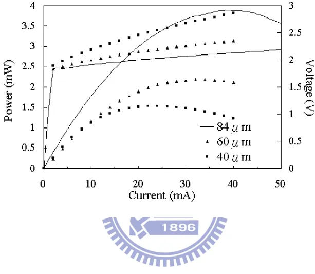
should be optimized for different requirements. Figure 2.8 described the typical
light-current-voltage (L-I-V) characteristics of RCLEDs with 84, 60, and 40 µm aperture sizes.
The output power of 84, 60 and 40 µm device without epoxy encapsulated under 20 mA
forward current operation were 3, 2 and 1.6 mW, respectively. From I-V curves, the devices
series resistance were 8.4, 14.7, 27 ohm, respectively. Although the 40 µm device presents the
lowest output power and the power saturate at lower driving current due to the high current
density, the maximum power was 1.6 mW and still suitable to transmitting data through 50 m
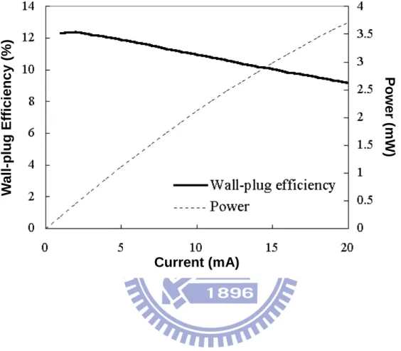
POF. Figure 2.9 shows the wall-plug efficiency and power characteristics of 84 µm devices.
The wall-plug efficiency was as high as 12% and the output power could achieve over 3.5
mW at 20 mA with epoxy encapsulated. R. Wirth et al., who had shown the output power and
maximum wall-plug efficiency of 2.9 mW and 9.5% from the same 84 µm emission aperture
size and 20 mA driving current and with epoxy [18]. The output power could be compared
with to other groups which have even larger aperture size under the equal measurement
conditions [14], [17]. In order to approach device temperature insensitive, properly detuning
the wavelength between resonant cavity and quantum well is necessary. The output power
variation versus detuning wavelength was shown in figure 2.10. The optimized wavelength
detuning is 15 nm and the emission power droop from 20°C to 85°C is less than -2dB. P.
The detuning wavelength will also affect the far field pattern and coupling efficiency in
POF applications, although POF has larger fiber core (1 mm) than glass optical fiber (GOF).
This investigation was presented that the device with 15 nm detuning wavelength exhibited
the far field pattern at 50% power angle of 134°. Figure 2.11 shows that the coupling
efficiency into 0.5 NA POF of transmitter remained a high value (>50%) in wide driving
current range (10 ~ 90 mA) due to the higher half power angle and output power. This
coupling efficiency could be compared with M. Dumitrescu et al. [13] report under the same
conditions of 0.5 NA POF and 84 µm devices, where their coupling efficiency was less than
35% from 0 mA to 40 mA operation current. Figure 2.12 shows the cut-off frequency -3dB
(f-3dB) of these three devices operated under 20 mA. It was demonstrated that the f-3dB for
aperture size of 84, 60 and 40 µm were 110.8, 228.6 and 313.3MHz, respectively. For
standard POF-based communications, the 84 µm RCLEDs cut-off frequency over 110 MHz
and the output power of 3.2 mW was demonstrated under 20 mA current injection. It was
demonstrated that the 84 µm RCLEDs devices could achieve to the IEEE 1394b s200
standard. In addition, the devices rise and fall-time is 2.86 ns and 1.08 ns respectively using
Hamamatsu Optical Oscilloscope C8188 test equipment. An open eye-diagram with error free
was obtained at Ibias=30 mA. Since the f-3dB of the 40 µm RCLEDs was 313MHz, the 40 µm
devices could achieve IEEE 1394b s400 standard. The 40 µm RCLEDs eye diagram achieved
622 Mbit/s and shown in figure 2.13. In order to achieve high speed RCLEDs, RCLEDs
epi-structure needs to modify. This carrier rate model in high speed RCLEDs has the
following formula [19]: ⋅ + − − = ∂ ∂ d q J Bn n t n 2 inject
τ
, (2-6)This is the dynamics of the electron carrier uniformly distributed in the active region of
coefficient, Jinject is the injection current density, and d is the thickness of active layer. From
this equation, there are several methods to modulation RCLEDs devices speed. Firstly, the
carrier lifetime τ could be reduced by inserting some non-radiate recombine centers in the
active region. But this method also decreased the internal efficiency of this structure, which is
not desirable. The second way is that increases the current density of injection or decreases
the size of emission window. However, these two ways will cause the power droop during
higher forward current injection. The last method is reducing the active layer thickness, it
could be increase the devices speed without sacrificing other performance. The cut-off
frequency and output power of 84 µm RCLEDs devices with single QW were obtained to be
235 MHz and 2 mW at 20 mA, respectively. This performance was suitable for IEEE 1394b
s400 standard applications. M.Guina et al. had also shown the data of bandwidth versus
current, and its cut-off frequency of 84 µm devices is 125 MHz under 20 mA current
operating [20]. In addition, an error free open eye diagram for the transceiver using single
QW RCLEDs devices at Ibias = 30 mA was obtained to be 500 Mbit/s data rate through a
graded-index POF over 50 m as shown in figure 2.14.
The high performances MBRCLEDs, having a high thermal conductivity Si substrate,
were fabricated via twice bonding technique of glue bonding and metal bonding processes. In
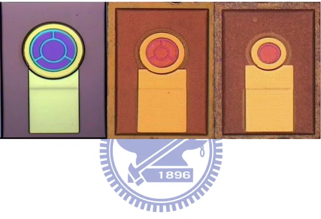
figure 2.15.1 shows the scanning electron microscope (SEM) photograph of the MBRCLEDs
devices with 300 x 300 µm2 dimensions. The figure 2.15.2 shows the MBRCLEDs
electron-luminescence (EL) state and light intensity profile. The emission area diameter is 84
µm and the dark area of the emission window is metal mesh line for current spreading. In the
RCLEDs devices applied requirements, the temperature insensitively properties is a key point.
In order to approach the temperature insensitivity, proper detuning the wavelength between
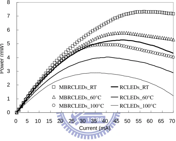
Figure 2.16 shows the light-current (L-I) curves of the MBRCLEDs and the RCLEDs were
operated at room temperature (RT), 60°C, and 100°C ambiance. It is observed that the output
power of MBRCLEDs decay were less than the RCLEDs. From RT to 100°C ambiance, the
output power drop of MBRCLEDs was -0.31, -1.78, and -2.5 dB under 20, 50 and 70 mA
current injection respectively. In addition, the output power droop of the RCLEDs were -1.75,
-3.03, -5.47 dB during 20, 50, and 70mA current injection respectively. The wall-plug
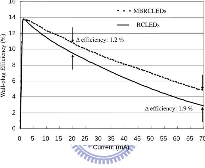
efficiency of the RCLEDs and the MBRCLEDs under room temperature operations were
shown in figure 2.17. The maximum wall-plug efficiency of MBRCLEDs was 13.7% under
2.5 mA current injection. In addition, the wall-plug efficiency difference (∆ efficiency) between
the MBRCLEDs and the RCLEDs under 20 and 70mA current operating were 1.2% and 1.9%,
respectively. Since the thermal conductivity of GaAs is poor than Si substrate, the self-heating
effect is relatively obvious in the RCLEDs especially. The phenomenon indicates that
although the structure had been optimized detuning wavelength but the self-heating still needs
a thermal conductivity path to release especially for high current injection. In junction
temperature (Tj) measurement, a pulsed generator (KEITHLEY Model 2520) was used to
obtain Vf variations in different current injection conditions with a short pulses time of 0.8
µsec. The junction temperature variations (
∆
Tj) versus forward voltage of the MBRCLEDs and the RCLEDs under pulsed current operation at room temperature was shown in figure2.18. It is significantly observed that the junction temperature of the RCLEDs is higher than
the MBRCLEDs, the caused of this result is higher thermal resistance of the GaAs material
than Si.
The RCLEDs performances will be degenerated with increasing temperature form
internal device, and lower internal quantum efficiency was induced due to the more leakage
current and non-radiative recombination. This serious leakage current in AlGaInP/ GaInP
MBRCLEDs fabrication processes, the epi-structure would undergo twice bonding processes,
which could be damage the thin epi-layers. The above results were demonstrated clearly that
the twice wafer bonding processes have not affected the epi-structure. Following, the
MBRCLEDs far-field patterns versus different temperature ambiance operating were shown
in figure 2.19. The MBRCLEDs were measured under 20 mA and without encapsulating
epoxy. The 50% power angle (half-center brightness or 50% of the full luminosity) of the
MBRCLEDs under RT and 80ºC is 134º and 126º, respectively. The cause of this result is
wavelength detuning between quantum-well and DBR resonance. This special wavelength
detuning (15nm) will affect the radiation pattern pass into rabbit ear and reduce the devices
temperature sensitively. From figure 2.19 results, the 50% power angle offset is only 8º under
RT to 80ºC ambiance operating due to the MBRCLEDs with a better thermal conductivity
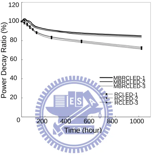
substrate. Figure 2.20 shows the life-time of the MBRCLEDs and the RCLEDs under a
condition of 85°C and 20 mA driving current. Both of the power reliability decay ratio were
less than 30% but the MBRCLEDs had a better reliability result due to an excellent thermal
conductivity substrate. In figure 2.21 shows the eye diagram measurements were performed to
estimate the ability of the MBRCLEDs for high-speed data communication under a condition
of devices were operated in 200MHz and 20mA driving current. Eye diagrams at RT and 80ºC
have a clear pattern and similar open eye diagram. As above-mentioned performances, the
MBRCLEDs are more suitable for working in high temperature ambiance than the RCLEDs
such as mobile components, industrial sensor and high-speed data rate transmission
2.5 Summary
In conventional GaAs substrate RCLEDs device summary, AlGaInP-based RCLEDs
with high power and high speed were demonstrated. In this investigation, the RCLEDs were
designed with different light-output aperture sizes 84, 60, and 40 µm, for different
applications of plastic optical fibers. The 40 µm aperture RCLEDs could be achieved that the
small-signal modulation bandwidths as high as 310 MHz at a forward current of 20 mA and
the output power as high as 1.5 mW. The devices with 84 µm apertures had an output power
of more than 3.5 mW at a driving current of 20 mA and a maximum efficiency of over 12 %
with an epoxy-encapsulated package. The devices with 40 µm apertures satisfied with the
IEEE 1394b s400 standard. Furthermore, the devices showed stable coupling efficiency for
various currents and output powers at different ambience temperatures. In addition, the
lifetime of devices is over 1300 h, and the power decay is less than 0.5 dB at 85°C for a 40
mA driving current.
Furthermore, we had developed the novel MBRCLEDs devices, having high
performances and replacing conventional GaAs substrate with a high thermal conductivity of
Si substrate. In 650 nm MBRCLEDs summary, MBRCLEDs has high performances, high
temperature insensitively, and high reliability have been successfully fabricated on Si
substrates by twice wafer bonding techniques. Although the RCLEDs epi-structure was
optimum designed for detuning wavelength, devices are still insufficient for high current
injection or high temperature operating. However, MBRCLEDs were based on this structure
and using metal bonding technique could improve devices performances especially in high
temperature ambiance. The junction temperature variations of the MBRCLEDs were
relatively smaller as compared with the RCLEDs. The MBRCLEDs with 84 µm apertures
provided high wall-plug efficiency of 13.7 % and a smaller power drooped of -0.31dB from
high reliability over 1000 hours and clearly eye diagram in high temperature operation. These
excellent performances of the MBRCLEDs devices should be suitable for high temperature
REFERENCE
[1] R. J. Ram, D. I. Babić, R. A. York, and J. E. Bowers, “Spontaneous emission in micro-cavities with distributed mirrors”, IEEE J. Quantum Electron., Vol.31, pp. 399,
1995.
[2] Y.-K. Song, Compound Semiconductor, Vol.6, pp. 53, 2000.
[3] N. E. J. Hunt, E. F. Schubert, R. A. Logan, and G. J. Zydzik, “Extremely narrow spectral widths from resonant cavity light-emitting diodes (RCLEDs) suitable for
wavelength-division multiplexing at 1.3 µm and 1.5µm”. 1992 International Electron
Devices Meeting (IEDM) San Francisco, CA, Dec. pp.13-16, 1992.
[4] E. F. Schubert, Y. H. Wang, A. Y. Cho, L. W. Tu, G. J. Zydzik, “Resonant Cavity Light-Emitting Diode”, Appl. Phys. Lett., Vol. 60, pp.921-923, 1992.
[5] E. F. Schubert, N. E. J. Hunt, R. J. Malik, M. Micovic, and D. L. Miller, “Temperature and modulation characteristics of resonant-cavity light-emitting diodes”, J. Lightwave
Technol., vol. 14, no. 7, pp. 1721–1728, 1996.
[6] H. De Neve, J. Blondelle, P. Van Daele, P. Demeester, R. Baets, G. Borghs, “Recycling of guided mode light emission in planar microcavity light emitting diodes”, Appl. Phys.
Lett., Vol. 70, pp.799-801, 1997.
[7] E. F. Schubert, N. E. J. Hunt, M. Micovic, R. J. Malik, D. L. Sivco, A.Y. Cho, and G. J. Zydzik, “Highly efficient light-emitting diodes with microcavities”, Science, Vol. 265,
pp.943, 1994.
[8] S. W. Chiou, Y. C. Lee, C. S. Chang, and T. P. Chen, “High-speed red RCLEDs and VCSELs for plastic optical fiber application”, Proceedings of SPIE, 5739, pp.129, 2005.
[9] J. F. Carlin, P. Royo, R. P. Stanley, R. Houdre, J. Spicher, U. Oesterle and M. Ilegems, “Design and characterization of top-emitting microcavity light-emitting diodes”,
Semicond. Sci. Technol., Vol.15, pp. 145, 2000.
[10] R. Wirth, C. Karnutsch, S. Kugler, W. Plass, W. Huber, E. Baur and K. Streubel: Proc.
POF2001, pp. 65, 2001.
[11] H. Benisty, H. De Neve, and C. Weisbuch, “Impact of planar microcavity effects on light extraction-Part I: Basic concepts and analytical trends”, IEEE J. Quantum Electron., Vol.
34, pp. 1612, 1998.
[12] R. Wirth, C. Karnutsch, S. Kugler, S. Thaler, and K. Streubel, “Red and Orange Resonant-Cavity LEDs”, Proceedings of SPIE, 4278, pp.43, 2001.
[13] M. M. Dumitrescu, M. J. Saarinen, M. D. Guina, and M. V. Pessa, “High-speed resonant cavity light-emitting diodes at 650 nm,” IEEE J. Selected Topics in Quantum Electron,
Vol. 8, pp. 219-224, 2002.
[14] K. Streubel, N. Linder, R. Wirth, and A. Jaeger, “High brightness AlGaInP light-emitting diodes,” IEEE J. Select. Topics Quantum Electronics, Vol.8, pp. 321-332, 2002.
[15] S. W. Chiou, Y. C. Lee, C. S. Chang, and T. P. Cheng, “High speed red RCLEDs and VCSELs for plastic optical fiber application,” SPIE Proc., Vol. 5739, pp. 129–133,
2005.
[16] M.-F. Huang, M.-L. Tsai, J.-Y. Shin, Y.-L. Sun, R.-M. Yang, and Y.-K. Kuo, “Optimization of active layer structures to minimize leakage current for an AlGaInP
laser diode,” Appl. Phys. A, Vol. 81, no. 7, pp. 1369–1373, 2005.
[17] P. Sipilä, M. Saarinen, M. Guina, V. Vilokkinen, M. Toivoneen, and M. Pessa, “Temperature behaviour of resonant cavity light-emitting diodes at 650 nm,” Semicond.
Sci. Technol., Vol. 15, pp. 418–421, 2000.
[18] R. Wirth, C. Karnutsch, S. Kugler, and K. Streubel, “High efficiency resonant cavity LED’s emitting at 650 nm”, IEEE Photonic Technol. Lett., Vol. 13, p. 421, 2001.
parallel Interconnections”, Chapter. 4, p.123, 2000.
[20] M. Guina, S. Orsila, M. Dumitrescu, M. Saarinen, P. Sipilä, V. Vilokkinen, B. Roycroft, P. Uusimaa, M. Toivonen, and M. Pessa, “Light-emitting diode emitting at 650 nm with
200-MHz small-signal modulation bandwidth,” IEEE Photon. Technol. Lett., vol. 12, no.
Figure 2.2: Intensity of the optical mode at the top mirror for an m=1 cavity. While the
reflectivity of the bottom DBRs was r22=1, the reflectivity r1 of the top DBRs was
Figure 2.3: Intensity of the optical mode at the top mirror for an m=1 cavity for various
detuning d. The reflectivity of the top DBRs was r12=0.6 and the bottom DBRs
Figure 2.4: The 650nm AlGaInP-based RCLEDs epi-structure.