n + -doped-layer-free microcrystalline silicon thin film transistors fabricated with the
CuMg as source/drain metal
M. C. Wang, T. C. Chang, Po-Tsun Liu, R. W. Xiao, L. F. Lin, Y. Y. Li, F. S. Yeh, and J. R. Chen
Citation: Applied Physics Letters 91, 022113 (2007); doi: 10.1063/1.2749847
View online: http://dx.doi.org/10.1063/1.2749847
View Table of Contents: http://scitation.aip.org/content/aip/journal/apl/91/2?ver=pdfcov Published by the AIP Publishing
Articles you may be interested in
Suppression of Schottky leakage current in island-in amorphous silicon thin film transistors with the Cu Cu Mg as source/drain metal
Appl. Phys. Lett. 91, 062103 (2007); 10.1063/1.2767147
Highly conductive n + hydrogenated microcrystalline silicon and its application in thin film transistors J. Vac. Sci. Technol. A 22, 991 (2004); 10.1116/1.1648674
Interfacial phase formation in Cu–Mg alloy films on SiO 2 J. Appl. Phys. 95, 3202 (2004); 10.1063/1.1647264
Kinetics of interfacial reaction in Cu–Mg alloy films on SiO 2 J. Appl. Phys. 95, 363 (2004); 10.1063/1.1630355
A self-passivated Cu(Mg) gate electrode for an amorphous silicon thin-film transistor Appl. Phys. Lett. 79, 3962 (2001); 10.1063/1.1424062
This article is copyrighted as indicated in the article. Reuse of AIP content is subject to the terms at: http://scitation.aip.org/termsconditions. Downloaded to IP: 140.113.38.11 On: Thu, 01 May 2014 00:22:33
n
+-doped-layer-free microcrystalline silicon thin film transistors fabricated
with the CuMg as source/drain metal
M. C. Wang
Department of Materials Science and Engineering, National Tsing Hua University, Hsin-Chui, 300 Taiwan, Republic of China
T. C. Changa兲
Department of Physics and Institute of Electro-Optical Engineering, Center for Nanoscience and Nanotechnology, National Sun Yat-set University, 70 Lien-hai Road, Kaohsiung, 804 Taiwan, Republic of China
Po-Tsun Liu
Department of Photonics and Display Institute, National Chiao Tung University, Hsin-Chu, 300 Taiwan, Republic of China
R. W. Xiao, L. F. Lin, Y. Y. Li, and F. S. Yeh
Institute of Electronics Engineering, National Tsing Hua University, Hsin-Chui, 300 Taiwan, Republic of China
J. R. Chen
Department of Materials Science and Engineering, National Tsing Hua University, Hsin-Chui, 300 Taiwan, Republic of China
共Received 24 April 2007; accepted 26 May 2007; published online 13 July 2007兲
The feasibility of using CuMg as source/drain metal electrodes for n+-doped-layer-free
microcrystalline silicon thin film transistors 共-Si: H TFTs兲 has been investigated. The Ohmic-contact characteristic has been achieved by using the CuMg alloy as source/drain metal. Furthermore, a wet etching process of Cu alloy source/drain metal has been completed by using the ferric chloride base etchant. The proposed-Si: H TFT has shown similar electrical characteristic with the-Si: H TFT with n+-doped layer. The experimental result also showed that the CuMg alloy
was suitable for the replacement of n+-doped layer in thin film transistor liquid-crystal displays.
© 2007 American Institute of Physics.关DOI:10.1063/1.2749847兴
Hydrogenated amorphous Si thin film transistors 共a-Si:H TFTs兲 have been widely used as switching devices for active matrix liquid crystal displays. The a-Si: H TFT is particularly advantageous to the production of large flat panel displays and facilitates mass production.1,2 The main objectives for flat panel display application are to enhance the field effect mobility and to reduce the off-state leakage current under backlight illumination.3Crystallized polycrys-talline silicon共poly-Si兲 thin film transistors with high mobil-ity are very attractive for peripheral circuit driver and switch-ing applications in active matrix backplanes for flat panel displays and imagers.4,5This is particularly true with active matrix organic light emitting diode displays. However, poly-Si suffers from high cost, complex processing, and sig-nificant nonuniformity over large area.
As a result, hydrogenated microcrystalline silicon has recently received considerable attention as a viable alterna-tive to its amorphous counterpart for large-area applications. In terms of TFT performance, not only a-Si: H TFTs employ-ing n+-Si: H as Ohmic contact layer show an improved electrical property6but also fully-Si: H TFTs are expected to yield higher field effect mobility and better electrical stability.7,8 More importantly,-Si: H films can be prepared using low thermal budget glow discharge gas decomposition method, which is also a standard industrial technique for a-Si: H deposition. However, small grain sizes 共a few tens
nanometer size兲, and poor quality at grain boundaries and at low thicknesses, are obstacles in achieving device grade
-Si: H films for high performance -Si: H TFTs. In addi-tion, most of the-Si: H TFTs reported have been fabricated using nonindustrial reactors such as very high frequency plasma enhanced chemical vapor deposition共PECVD兲,7 hot wire CVD,9 and electron cyclotron resonance CVD.10 It is very desirable to achieve high grade TFTs using intrinsic and doped-Si: H films by the standard PECVD compatible to mass production. Therefore, the direct deposition of high quality -Si thin films is a promising alternative for high mobility TFTs.11–13 On the other hand, the Ohmic-contact characteristic of the-Si: H was also important for the ap-plication of-Si: H TFTs. Compared to its amorphous coun-terpart, highly doped microcrystalline silicon共n+--Si: H兲 is
attractive due to its much higher conductivity and doping efficiency.6However, the thickness of-Si: H was also lim-ited by n+-etching process for the production concern. In this letter, the CuMg alloy was used as source/drain metal and provided self-aligned Ohmic-contact characteristic.
A 100-nm-thick MoW gate electrode was deposited and patterned on the glass substrate. It was followed that the back-channel-etched共BCE兲-Si: H TFT devices were fabri-cated by depositing a 100-nm-thick silicon oxide共SiOx兲, and
a 100-nm-thick -Si: H active layer subsequently on the MoW gate using PECVD method. However, the n+-doped-layer was not deposited in the proposed structure compared with the conventional process. After the -Si: H
a兲Electronic mail: [email protected]
APPLIED PHYSICS LETTERS 91, 022113共2007兲
0003-6951/2007/91共2兲/022113/3/$23.00 91, 022113-1 © 2007 American Institute of Physics
This article is copyrighted as indicated in the article. Reuse of AIP content is subject to the terms at: http://scitation.aip.org/termsconditions. Downloaded to IP: 140.113.38.11 On: Thu, 01 May 2014 00:22:33
active islands were patterned, a thin CuMg alloy layer 共300 nm兲 was deposited by dc magnetron sputtering a 99.99% purity level of CuMg alloy target共4.5 at. % Mg兲 at room temperature. The sputtering condition of CuMg alloy was as follows: the base pressure of the deposition chamber was 7.0⫻10−7 torr, the Ar pressure was 6 mtorr, the
sputter-ing power was 1500 W, and the substrate temperature was at room temperature. The CuMg metal films were patterned by wet etching process to form source/drain electrodes. The wet etching process of the CuMg alloy structure was also com-pleted by introducing the ferric chloride base etchant, typi-cally used in printed circuit boards. The etch rate of CuMg film was about 1.9 nm/ s and the critical dimension loss was less than 1.4m. The detail process flow was illustrated in Fig.1. For comparison, the BCE-Si: H TFT devices with n+-a-Si: H layer were also fabricated by depositing a 100-nm-thick SiOx, a 100-nm-thick-Si: H active layer, and
a 50-nm-thick n+-a-Si: H layer subsequently on the MoW
gate using PECVD method. After the-Si: H active islands were patterned, a 300-nm-thick sputter-deposited Al layer was patterned by wet etching process to form source/drain electrodes. Finally, the n+-a-Si: H layer on the TFT channel
region was etched via the source/drain pattern electrodes as the etching mask. The channel length and width were 12 and 36m, respectively. The-Si: H film was confirmed by Ra-man analysis and the scanning electron microscopy共SEM兲. The annealing stability of CuMg alloy as source/drain metal was also tested at 300 ° C for 30 min in a vacuum chamber. The electrical measurement was carried out at an HP 4156C precision semiconductor parameter analyzer.
Figure 2 showed the Raman analysis of -Si: H. We deposited -Si: H films at 400 ° C using a standard large-area single-chamber 13.56 MHz PECVD system by high H2
dilution of SiH4 process gas 共H2/ SiH4= 80兲. The Raman peaks of the film were very sharp at 510 cm−1. The full width
half maximum共FWHM兲 was measured about 11 cm−1. The Raman peak was deconvoluted using a Lorenztian multipeak function. The crystal fraction was calculated using the for-mula共Ic+ I兲/共Ic+ I+ Ia兲 where Icis the area of crystalline
peak共520 cm−1兲, I
is the area of the microcrystalline peak
共510 cm−1兲, and I
a is the area of the amorphous peak
共480 cm−1兲.14
The resulting -Si: H film shows a Raman crystallinity共XC兲 about 70% 共Fig. 2兲. The films were
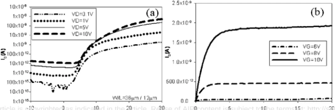
ana-lyzed for their surface morphology using SEM. As shown in the inset of Fig.2, presence of small grains can be observed in the SEM image. The size of the grains and the grain size distribution across the film surface vary depending on spe-cific deposition conditions of-Si: H and pretreatments on the silicon oxide surface. The performance of a bottom gate TFT with back-channel etch is very sensitive to the grain size distribution uniformity. It was, therefore, important to de-velop the thin film with uniform grain structure. The grain size of the -Si: H using SEM images was about 80 nm. Figure3共a兲shows the transfer characteristics of the n+-doped layer-free -Si: H TFT with the CuMg source/drain metal after annealing at high temperature process.15,16 The pro-posed n+-doped layer-free-Si: H TFT with the CuMg alloy
source/drain metal demonstrated the field-effect mobility of 0.1 cm2/ V s, the subthreshold slope of 1.26 V/decode, and
the threshold voltage of 5.02 V. The mobility was extracted from the linear ID-VGplot, where the drain voltage 共VD兲 is
0.1 V, and the threshold voltage was extracted from the
lin-FIG. 1. Detail process flow of the proposed-Si: H TFT with the CuMg source/drain and back-channel-etched 共BCE兲 inverted-staggered TFT structure.
FIG. 2. Raman analysis of-Si: H and a-Si: H film. The inset shows the SEM surface profile of-Si: H.
FIG. 3. 共a兲 Transfer characteristics 共ID-VG curve兲 of n+-doped-layer free -Si: H TFT with the CuMg source/ drain metal after the 300 ° C 30 min annealing process in the vacuum chamber. The channel length and width are 12 and 36m, respectively. 共b兲 Output characteristics 共ID-VD
curve兲 of n+-doped-layer-free-Si: H
TFT with the CuMg source/drain metal after the 300 ° C, 30 min anneal-ing process in the vacuum chamber.
022113-2 Wang et al. Appl. Phys. Lett. 91, 022113共2007兲
This article is copyrighted as indicated in the article. Reuse of AIP content is subject to the terms at: http://scitation.aip.org/termsconditions. Downloaded to IP: 140.113.38.11 On: Thu, 01 May 2014 00:22:33
ear ID-VGplot, where the VD= 0.1 V. The a-Si: H-like
char-acteristic was due to 20-nm-thick a-Si: H incubation layer in bottom-gate structure. The electrical characteristic of-Si: H TFT with the n+-doped layer also showed the same
a-Si: H-like characteristic. Therefore, the a-Si: H-like char-acteristic was not due to the CuMg alloy as source/drain metal. Furthermore, the output characteristics of -Si: H TFT are also shown in Fig.3共b兲, measured at the gate volt-ages sweeping from 6 to 10 V by a voltage step of 2 V. It is shown no current crowding effect appears in the CuMg alloy source/drain metal -Si: H TFT device. This indicates also the voltage applied on the TFT was not limited by the source/ drain contact resistance. According to pervious report, the Ohmic behavior is observed for metals having work function 共⌽m兲 lower than the electronic affinity 共s兲 of the Si film
共s⬃4.0±0.1 eV兲. Because the ⌽mof Mg was 3.46 eV, the
Mg was easily to form the Ohmic contact with -Si: H.17 The -Si: H layer also reduced the contact resistance. Ac-cording to previous report,18 the carrier transfer mechanism across the barrier is a thermally activated process, the contact resistance will be proportional to the Si film resistivity. As s result, the lower Si film bulk resistivity is resulted in lower contact resistance. The similar electrical characteristic of
-Si: H TFT with n+-a-Si doped layer also indicated the
good Ohmic-contact characteristic of CuMg alloy structure. The-Si: H TFT device without n+-a-Si doped layer has been developed in this work. The CuMg alloy film acting as the source/drain electrode could replace the n+-a-Si doped
layer due to the lower work function 共⌽m兲 of Mg than the
electronic affinity共s兲 of Si film and the use of-Si layer to
reduce the contact resistance. Compared to the-Si: H TFT with n+-doped layer, the -Si: H TFT with CuMg alloy source/drain metal exhibited the similar electrical perfor-mance. For the production concern, the CuMg source/drain metal could be applied for the TFT with the n+-doped
layer-free process and provided self-aligned Ohmic-contact characteristic.
This work was partially supported by National Science Council, the Republic of China under Contract Nos. NSC-94-2120-M-110-005, NSC94-2215-E-009-031,
NSC-95-2120-M-110-003, and NSC 95-2221-E-009-254-MY2, and MOEA Technology Development for Academia under Project 94-EC-17-A-07-S1-046 and MOE ATU Program. Also, the authors thank the Taiwan TFT LCD Association 共TTLA兲, and AU Optronics Corp. 共AUO兲, Taiwan, for their support.
1W. E. Howard, J. Soc. Inf. Disp. 3, 127共1995兲.
2S. Venkatesan, A. V. Gelatos, V. Misra, B. Smithe, R. Islam, J. Cope, B.
Wilson, D. Tuttle, R. Cardwell, S. Anderson, M. Angyal, R. Bajaj, C. Capasso, P. Crabtree, S. Das, J. Farkas, S. Filipiak, B. Fiordalice, M. Freeman, P. V. Gilbert, M. Herrick, A. Jain, H. Kawasaki, C. Kiing, J. Klein, T. Lii, K. Reid, T. Saaranen, C. Simpson, T. Sparks, P. Tsui, R. Venkatraman, D. Watts, E. J. Weitzman, R. Woodruff, I. Yang, N. Bhat, G. Hamilton, and Y. Yu, Tech. Dig. - Int. Electron Devices Meet. 1997, 769.
3D. Edelstein, J. Heidenreich, R. Goldblatt, W. Cote, C. Uzoh, N. Lustig, P.
Roper, T. McDvitt, W. Motsfiff, A. Simon, J. Dukovic, R. Wachnik, H. Rathore, R. Shultz, L. Su, S. Luce, and J. Slattery, Tech. Dig. - Int. Elec-tron Devices Meet. 1997, 773.
4M. Sekiya, M. Hara, N. Sano, A. Kohno, and T. Sameshima, IEEE
Elec-tron Device Lett. 15, 69共1994兲.
5J. Jang, J. Y. Oh, S. K. Kim, Y. J. Choi, S. Y. Yoon, and C. O. Kim, IEEE
Electron Device Lett. 395, 481共1998兲.
6C. H. Lee, D. Striakhilev, and A. Nathan, J. Vac. Sci. Technol. A 22, 991
共2004兲.
7M. Mulato, Y. Chen, S. Wagner, and A. R. Zanatta, J. Non-Cryst. Solids 266, 1260共2000兲.
8P. Roca I Cabarrocas, S. Kalache, R. Vanderhghen, and Y. Bonnassieux,
SID 03 Digest共Society for Information Display, San Jose, CA, 2003兲, p. 1096.
9H. Meiling, A. M. Brockhoff, J. K. Rath, and R. E. I. Schropp, J.
Non-Cryst. Solids 227-230, 1202共1998兲.
10A. T. Krishnan, S. Bae, and S. J. Fonash, IEEE Electron Device Lett. 22,
399共2001兲.
11T. Nagahara, K. Fujimoto, N. Kohno, Y. Kashiwagi, and H. Kakinoki, Jpn.
J. Appl. Phys., Part 1 31, 4555共1992兲.
12I. C. Cheng and S. Wagner, Appl. Phys. Lett. 80, 440共2002兲.
13L. Teng and W. A. Anderson, IEEE Electron Device Lett. 15, 399共2003兲. 14M. Lisachenko, M. Kim, C. Kim, S. W Lee, K. B. Kim,J. W. Seo, K. Y.
Lee, H. D. Kim, and H. K. Chung, SID 06 Digest共Society for Information Display, San Jose, CA, 2006兲, p. 250.
15W. H. Lee, B. S. Cho, B. J. Kang, H. J. Yang, J. G. Lee, I. K. Woo, S. W.
Lee, J. Jang, G. S. Chae, and H. S. Soh, Appl. Phys. Lett. 79, 3962共2001兲.
16P. S. Shin, T. C. Chang, S. M. Chen, M. S. Feng, D. Z. Peng, and C. Y.
Chang, Surf. Coat. Technol. 108, 588共1998兲.
17H. Matsuura, T. Okuno, H. Okushi, S. Yamasaki, A. Matsuda, N. Hata, H.
Oheda, and K. Tanaka, Jpn. J. Appl. Phys., Part 2 22, L197共1983兲.
18J. Kanicki, Appl. Phys. Lett. 53, 1943共1988兲.
022113-3 Wang et al. Appl. Phys. Lett. 91, 022113共2007兲
This article is copyrighted as indicated in the article. Reuse of AIP content is subject to the terms at: http://scitation.aip.org/termsconditions. Downloaded to IP: 140.113.38.11 On: Thu, 01 May 2014 00:22:33