www.nature.com/scientificreports
Bulk vs. Surface Structure of 3d
Metal Impurities in Topological
Insulator Bi
2
Te
3
B. Leedahl
1, D. W. Boukhvalov
2,3, E. Z. Kurmaev
4,5, A. Kukharenko
5, I. S. Zhidkov
5,
N. V. Gavrilov
6, S. O. Cholakh
5, P. Huu Le
7,8, C. Wei Luo
7& A. Moewes
1Topological insulators have become one of the most prominent research topics in materials science in recent years. Specifically, Bi2Te3 is one of the most promising for technological applications due to its conductive surface states and insulating bulk properties. Herein, we contrast the bulk and surface structural environments of dopant ions Cr, Mn, Fe, Co, Ni, and Cu in Bi2Te3 thin films in order to further elucidate this compound. Our measurements show the preferred oxidation state and surrounding crystal environment of each 3d-metal atomic species, and how they are incorporated into Bi2Te3. We show that in each case there is a unique interplay between structural environments, and that it is highly dependant on the dopant atom. Mn impurities in Bi2Te3 purely substitute into Bi sites in a 2+ oxidation state. Cr atoms seem only to reside on the surface and are effectively not able to be absorbed into the bulk. Whereas for Co and Ni, an array of substitutional, interstitial, and metallic configurations occur. Considering the relatively heavy Cu atoms, metallic clusters are highly favourable. The situation with Fe is even more complex, displaying a mix of oxidation states that differ greatly between the surface and bulk environments.
The Bi-chalcogenides such as Bi2Te3 and Bi2Se3 have long been known for their thermoelectric properties1, 2,
but recently they have gained a great deal of attention as three-dimensional topological insulators with a large band gap and a single Dirac cone on the surface3–8. Additionally, the introduction of magnetic impurities into
Bi-chalcogenides can break time-reversal symmetry and open an energy gap at the Dirac point of the surface states9–11. Recently, Bi
2Te3 and related systems with dilute doping of 3d-metal atoms (Ti, V, Cr, Mn, and Fe) have
been found to have ferromagnetic transitions at low temperatures. Bi2−xMnxTe3 was found to have a Curie
tem-perature TC around 10 K for x = 0.0212. For larger doping of thin films of Sb2−xVxTe3, with x = 0.35, TC increases
to 177 K and for SbCrxTe3 with x = 0.59 TC increases to 189 K13 which is close to that of more traditional dilute
magnetic semiconductors (DMS)14.
Most DMS materials are crystallized in zinc-blende or wurtzite crystal structures with tetrahedral bonds between atoms. In this respect Bi2Te3 is different, its tetradymite-type structure has atoms that form in octahedral
coordination. When transition metal atoms are introduced to the tetradymite-type structure, there are various possible oxidation states they may exist in. In addition, the spin-orbit interaction is more complicated due to the expanded octet bonding where not only p-orbitals, but also d-orbitals join the hybridization. The relatively sophisticated tetradymite structure leaves a lot of structural and chemical factors available to be tweaked. This induces even more complicated structural configurations when impurity atoms are introduced, and as a result, create new, unexpected electronic and magnetic properties. In the present paper the local crystal and electronic structure of 3d-impurities (Cr, Mn, Fe, Co, Ni, Cu) in Bi2Te3 thin films are studied using x-ray photoelectron 1Department of Physics and Engineering Physics, University of Saskatchewan, 116 Science Place, Saskatoon, Saskatchewan, S7N 5E2, Canada. 2Department of Chemistry, Hanyang University, 222 Wangsimni-Ro, Seoul, 04763, Republic of Korea. 3Theoretical Physics and Applied Mathematics Department, Ural Federal University, Mira Street 19, 620002, Yekaterinburg, Russia. 4M.N.Mikheev Institute of Metal Physics of Ural Branch of Russian Academy of Sciences, S. Kovalevskoi 18 str., 620990, Yekaterinburg, Russia. 5Institute of Physics and Technology, Ural Federal University, Mira 19 St., 620002, Yekaterinburg, Russia. 6Institute of Electrophysics, Russian Academy of Sciences-Ural Division, 620016, Yekaterinburg, Russia. 7Department of Electrophysics, National Chiao Tung University, Hsinchu, 30010, Taiwan, ROC. 8Faculty of Basic Sciences, Can Tho University of Medicine and Pharmacy, 179 Nguyen Received: 22 March 2017
Accepted: 7 June 2017 Published: xx xx xxxx
www.nature.com/scientificreports/
spectroscopy (XPS), x-ray ray absorption (XAS), and resonant x-ray emission (RXES) techniques. The experi-mental spectra are compared with density functional theory (DFT) calculations of formation energies for differ-ent configurations of the dopant atoms. These techniques are powerful in that they are non-invasive and able to distinguish between bulk and surface states, key to the study of topological insulators15.
Experiment and Calculation Details
Bi2Te3 thin films were grown on an Al2O3(0001) substrates via pulsed laser deposition using a stoichiometric
Bi2Te3 target with a purity of 99.99%16. The KrF-pulsed laser fluence and repetition rate were 3.7 J/cm2 and 4 Hz,
respectively. The base pressure of the growth chamber was below 2 × 10⁻⁶ Torr. Before loading into the chamber,
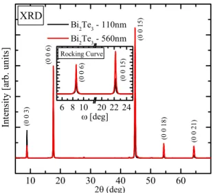
the substrates were first cleaned using ultrasonication in acetone, methanol, and then deionized water for 30 min-utes. The pressure in the chamber was maintained at 0.35 Torr while argon gas was introduced throughout the deposition process. The optimized substrate temperature was 260 °C. The deposition times were 5 minutes and 25 minutes to grow the films with thicknesses of approximately 110 and 560 nm, respectively. The orientation and crystallinity of Bi2Te3 films were determined using x-ray diffraction (XRD) with Cu Kα radiation (8048 eV); the
results are displayed in Fig. 1.
The implantation of ions in Bi2Te3 thin film samples was carried out in a vacuum chamber that was
evacu-ated to a residual pressure of 3 × 10⁻³ Pa. An ion beam with an energy of 30 keV was created at a source cathode
by vaporizing the metal with an electric arc. The ions were then used to irradiate the sample in a pulsed mode (25 Hz). After 38 minutes of exposure the sample had an ion fluence (integrated flux over time) of 1 × 1017 cm−2.
For ion implantation Cr, Mn, Fe, Ni, Co and Cu metals were used.
X-ray photoelectron spectroscopy (XPS) core-level measurements were performed using a spectrometer with an energy analyzer working in the range of binding energies from 0 to 1400 eV. The samples were intro-duced to vacuum (10−7 Pa) for 24 hours prior to measurement, and only samples whose surfaces were free from
micro-impurities were measured and reported herein. The XPS spectra were recorded using Al K α (1486.6 eV) x-ray emission photons; the spot size was 100 μm; the energy resolution is ΔE < 0.5 eV; and typical signal to noise ratios were greater than 10000:3. The x-ray absorption spectroscopy (XAS) measurements were taken at Beamline 8.0.1 at the Advanced Light Source (ALS), and the REIXS and SGM beamlines, the latter two being at the Canadian Light Source. Finally, the x-ray emission (XES) measurements were performed using Beamline 8.0.117.
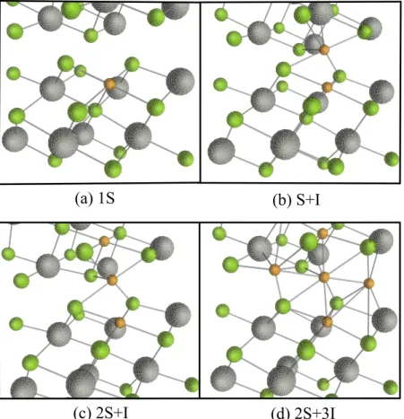
To simulate 3d-metal impurities in Bi2Te3 we applied the pseudo-potential code SIESTA18. For our purposes
a supercell containing 60 atoms (Bi24Te36) was adequate; this provides a sufficient distance between embedded
impurities. We calculated the formation energies for four possible combinations of impurities: a single substi-tutional impurity of bismuth (1S, Fig. 2a), a combination of substitutional impurity and embedded one into the interlayer space (S + I, Fig. 2b), a combination of two substitutional and one interstitial impurities (2S + I, Fig. 2c) and a configuration obtained by adding two interstitial atoms to the previous configuration (2S + 3I, Fig. 2d).
The crystal field multiplet calculations in this work use the algorithm initially formulated by Cowan, and the working code subsequently expanded on by Haverkort and Green et al.19–22. The free parameters include
the crystal field strength (from which the local symmetry can be deduced), oxidation state, and the scaling of the intra-atomic Coulomb and exchange (Slater) integrals. The dipole transition matrix elements calculated by this code are then used in the Kramers-Heisenberg equation to simulate spectra23. All spectra are broadened by
convolutions of a Lorentzian function (to simulate lifetime broadening), and a Gaussian function (to simulate experimental broadening) to match experimental conditions.
Figure 1. X-ray diffraction results show the high quality crystallinity of the Bi2Te3 thin films created using
www.nature.com/scientificreports/
XPS Measurements
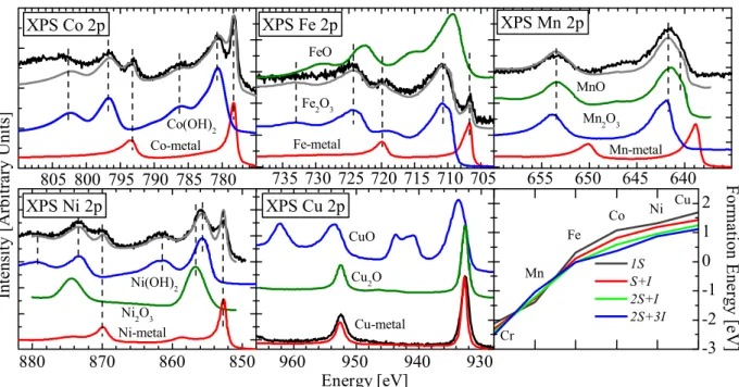
Using Al K α photons, XPS allows one to probe the binding energies of a transition metal’s 2p electrons; this technique is primarily sensitive to the surface oxidation state of the atoms. The surface sensitivity is in the range of ≈5 nm, due to the mean free path of escaping electrons. Furthermore, if the metal atoms exist in multiple oxida-tion states simultaneously, we will observe a superposioxida-tion of the peaks from the corresponding oxidaoxida-tion states in our sample. Of note is that Cr XPS data was not possible due to the overlap of Cr 2p and Te 3d binding energies, coupled with the dilute nature of Cr atoms, it was not feasible to subtract out the much stronger Te 3d signal.
Shown in Fig. 3 are our XPS measurements determining the 2p3/2,1/2 binding energies of the dopant atoms in
Bi2Te3. For each dopant atom except Mn, there is an obvious contribution from the metallic phase of each element.
This corresponds to the peak position in the metallic reference spectra also appearing in the doped Bi2Te3 samples
(indicated with vertical dashed lines in each plot of Fig. 3). This agrees with what we would roughly expect to see when considering our calculations of formations energies (Table 1). For each element we see that the clustering of dopant atoms (and hence the formation of metal-like regions, corresponding to 2S + 3I and 2S + I defects), are quite favourable (see lower right panel of Fig. 3 for formation energies of defects), especially in the cases of the heavier elements Co, Ni, and Cu. These defects can be thought of as the tendency for the transition metal atoms to cluster together (see Fig. 2c,d). On the other hand, each doped sample also contains ionized dopants that reside in the Bi2Te3 lattice that do not form metallic clusters.
By normalizing the reference XPS spectra to have equal 2p3/2 and 2p1/2 edge jumps, we were able to take a
linear combination of these to obtain good approximations for proportion of each oxidation state for each metal in Bi2Te3. The grey curves in Fig. 3 are the linear combination results; in all cases the match with the experimental
spectrum is remarkably good. We have summarized the results and percentages of each oxidation state for each dopant in Table 1.
Manganese is specifically of interest because of its unique incorporation into Bi2Te3. When component
oxida-tion states were analyzed, we found that there is virtually no metal-like signal, and 91% Mn2+. This means that in
the case of Mn doping, the cation substitution Mn2+ → Bi3+) is the primary defect. Our DFT calculations in the
lower right panel of Fig. 3 support this view for Mn as well. It is the only dopant for which the formation energy of a substitutional impurity is the most favourable. In general our DFT calculations support the observed XPS
Figure 2. The four defect structures for which formation energies were calculated for in the Bi2Te3 crystal
lattice. (a) 1S − a substitutional transition metal dopant residing in a Bi crystal site. (b) S + I − substitutial and interstitial atoms location adjacent to one another. (c) 2S + I − further clustering of metallic atoms.
(d) 2S + 3I − this defect corresponds to large amount of metallic atoms clustering together, observed as the formation of metallic bonds. Bismuth atoms are displayed in grey, tellurium in green, and transition metal dopants in orange.
www.nature.com/scientificreports/
of metallic cluster formation. That is, metallic clusters tend to form when the cluster-like 2S + 3I defects are suffi-ciently lower in energy than 1S defects, and the reverse is true as well, as shown in the case of manganese.
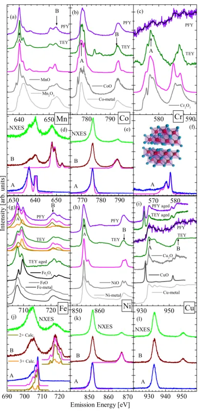
X-ray Absorption and Emission
Further x-ray measurements complement our XPS findings, these are displayed in Fig. 4. When coupled with crystal field calculations, these measurements can be used to deduce the local symmetry of the dopant ions, as well as their oxidation state. By achieving agreement between calculation and experiment, we can use the parameters used in the calculation to extract real physical results. Another important distinction to consider is that the XAS measurements were performed in both total electron yield (TEY) mode, only sensitive to the first ≈5 nm of the sample surface, and the more bulk sensitive partial fluorescence yield (PFY). XES measurements are inherently bulk sensitive (≈100 nm) similar to PFY, due to the greater escape depth of photons as compared to electrons.
For comparison, we have displayed the absorption spectra of common oxides and metals next to the spectra of each of the dopants in Fig. 4. Since each oxidation state for each 3d transition metal atom has a vastly different shape, this comparison alone can determine the ion’s valency. In each case the calculation (pink) was performed for the primary oxidation state that was found via the XPS data. In general, they adequately agree with the exper-imental spectra, despite the fact of the existence of some portion of pure metallic bonding in each sample. This is because metallic absorption spectra are rather broad and featureless, whereas the rich spectra of charged tran-sition metal atoms still shines through on top of this. Below we will discuss each dopant in turn and some slight exceptions to the above general statements.
Figure 3. XPS spectra for doped samples. Black curves are 2p excitations of the TM dopant atoms in Bi2Te3.
Grey curves are a linear combination of standard references. Table 1 indicates the approximate proportion of each oxidation state the dopants are in. The lower right panel are DFT calculated formation energies for each dopant for four types of defects.
0 (metallic) 2+ 3+ Cr — — — Mn 0 88 12 Fe 25 0 75 Co 46 54 0 Ni 30 68 2 Cu 100 0 0
Table 1. The XPS spectra in Fig. 3 were decomposed into their component oxidation states through a linear combination of common oxides and metals. The tabulated values in this table indicate the percentage of each oxidation state found for each dopant metal on the Bi2Te3 surface. The corresponding linear sum is also plotted
www.nature.com/scientificreports/
Cobalt.
In the case of cobalt (Fig. 4b), which has a high percentage of metallic bonding, the agreement between calculation and experiment is least satisfying (due to a large Co-metal contribution), Despite this,Figure 4. X-ray absorption and emission at the transition metal L-edges along with calculated spectra (pink).
The Bi2Te3: TM XAS spectra are shown in black with standard oxide references in grey for comparison. Panels
(a–c) and (g–i) contain the XAS spectra, while beneath each is the corresponding element’s XES spectra in panels d–f and j–l, respectively. In panel (g), the iron calculations are shown in orange and dark yellow, with the linear sum of the two shown in pink. A thorough discussion of each element’s spectra is given separately in the main text. High quality Ni, Co, Fe metal XAS reference spectra were taken from ref. 24.
www.nature.com/scientificreports/
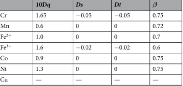
differences between these two spectra illustrate that cobalt in the bulk of the sample tends more towards a metallic state, while on the surface it is still largely found in its 2+ state. This is evident from the much more rich TEY spectrum, and in accordance with our XPS results above, which stated that 54% of Co atoms are in a 2+ state. From the agreement with our calculation we can deduce that cobalt in the the sample that is not metallic is in very nearly a perfect octahedral coordination. The splitting of the eg and t2g 3d orbital is given by the 10Dq parameter,
and since 10Dq = 0.9 eV; Ds = Dt = 0, we can be sure it is octahedrally coordinated.
Chromium.
A similar analysis between the topological surface and deeper bulk environments for other dopants can also be done. In the case of chromium, the dopant atoms effectively only reside on the surface and are not incorporated into the host lattice at all during the ion implantation process, despite being subject to the same fluence. We have two pieces of evidence to support this: (1) the lack of any meaningful PFY signal; in Fig. 4c the PFY is extremely weak; (2) the XES had an order of magnitude less counts per second for Cr as compared to the other samples (hence why only one excitation is shown in Fig. 4f; it was not possible to obtain more data due to the time length of the measurements). In both cases it is likely that the emitted photons almost entirely originate from the thin surface layer (in which Cr3+ is nicely substituted into Bi2Te3). Hence, the bulk of the sample must
have been effectively void of Cr ions.
As evidenced by the strong TEY signal, we are certain that the surface contains Cr3+ ions in a slightly warped
octahedral environment (see Table 2 for crystal field parameters). Therefore, we have found a profound difference in the assimilation environments for Cr atoms in Bi2Te3. Cr atoms appear completely comfortable in a 3+
octa-hedral surface environment, but will not form in the bulk of the crystal lattice. The lack of bulk Cr can possibly be explained by its small ionic radius, because it is smaller than the other transition metal dopants used here, it may have difficulty finding a low energy state to reside in, and it is effectively expelled from the lattice.
Nickel.
Nickel doping is quite similar to cobalt in that a substantial fraction of the dopant atoms prefer to metallically cluster together. However, in this incidence the TEY and the PFY for Ni (Fig. 4h) show nearly identi-cal results, with spectra that are a mix between that of Ni-metal and NiO, in agreement with the XPS data. That is, there is a substantial proportion of metallic Ni clusters present. The main conclusion here is that there is no dif-ference between the surface and bulk Ni incorporation, in both locations effectively identical results were found.Manganese.
The most consistent dopant is manganese. In this case all of the DFT, XPS, TEY, and PFY results support the same conclusion: that Mn2+ is integrated into the host crystal in substitutional octahedral positions, butin an environment with a much lower crystal field strength than MnO (which is 1.0 eV)25, due to the larger spatial
environment the Mn ions have in our case. In a past study it was shown that pristine Bi2Te3 and Mn doped Bi2Te3
have have measurably different conductive properties26. This difference must not originate due to metallic Mn,
and in accordance with the cited study, there is no need to invoke any special inherent surface states to explain the conductive behaviour in the doped sample. Effectively, when incorporating Mn into Bi2Te3, both the surface and
the bulk environments react identically, and any topological differences must be a result of the host material itself.
Copper.
We found that copper undergoes a large scale transformation with age in Bi2Te3. Initially it was foundto be in a purely metallic state; this was confirmed by the XPS measurements as well as both TEY and PFY in Fig. 4i. However, upon exposure to atmospheric conditions for one year, a substantial fraction of the metallic clusters have converted to 2+ ions. This is evident from the followup absorption spectra taken (shown as “aged”), which show substantial contributions to the signal in the same energetic locations as that of CuO. We believe we can dismiss simple oxidation and the formation of CuO because the bulk of the sample also shows this same phenomena, and the exposure with air to the bulk of the sample is negligible. Also, surface oxidation generally takes place on the scale of only a few minutes27, and the initial XPS and XAS measurements showed no sign of
this (after the samples were already exposed to air for months). Hence, we can conclude that the bulk and surface properties of Cu dopants in Bi2Te3 are effectively identical, and furthermore they age and change identically,
and that no special surface states for Cu ions exist upon ion implantation. Note that copper spectra show no fine multiplet structure because of its full 3d shell (the same holds for d9 in the case of Cu2+), so calculations offer no
extra insight in this specific case.
Iron.
Lastly, iron is the most complicated case as it was necessary to use a combination of oxidation states on both the surface and in the bulk. However, the ratio of 2+:3+ Fe ions on the surface and in the bulk of the material is much different. If we first consider the TEY in Fig. 4g and compare it to the XPS in Fig. 3 we discover10Dq Ds Dt β Cr 1.65 −0.05 −0.05 0.75 Mn 0.6 0 0 0.72 Fe2+ 1.0 0 0 0.7 Fe3+ 1.6 −0.02 −0.02 0.6 Co 0.9 0 0 0.75 Ni 1.3 0 0 0.75 Cu — — — —
Table 2. Shown are the crystal field parameters for the calculations in pink in Fig. 4. The units for 10Dq, Ds, and
www.nature.com/scientificreports/
that there are some conflicting results. To contrast these, we examine further XAS measurements done a year after the initial ones to reveal that the surface undergoes a slow aging process. Initially, our XPS results showed that the surface contained 75% Fe3+ and 25% metallic Fe (Table 1). Then upon aging for six months our TEY
measurements indicate that this ratio has fallen to about 58% Fe3+, while the remaining 42% can be classified as
Fe2+. This is apparent from our linear sum of Fe2+ and Fe3+ calculations in Fig. 4g; one can see that the sum of
the calculations is a near perfect fit for the experimental TEY spectrum. To test for reproducibility, further TEY measurements were done another year later (TEY aged), and they unambiguously show that the iron on the sur-face of the sample has become nearly entirely 3+. Hence, we have shown that the Bi2Te3 surface enables a slow
transformation of Fe atoms’ oxidation state toward 2+ , given sufficient time.
What is interesting is how the bulk of Bi2Te3 reacts in a manner very contrary to its surface. In this case, bulk
sensitive PFY measurements taken 18 months apart show no change. We also found that contrary to the surface, it is Fe2+ ions that are much more inclined to reside in the bulk. To illustrate this, a similar analysis as above was
done. The 2+ and 3+ calculations together show that the ratio of 2+:3+ is 60:40 in the bulk. It appears clear that in the case of iron dopants in Bi2Te3 the surface states are vastly different from that of those in the bulk, and
undergo different incorporation mechanisms, as well as different aging effects.
Conclusion
In closure, we have studied the differences between dopant atoms on the surface and in the bulk of what is known to be a promising material for topological technologies. The inherent differences between the bulk and surface structural properties can manifest themselves upon examining how transition metal dopants assimilate into the host lattice. This method of doping with 3d metals is an oft use way of fine-tuning a material’s electronic and magnetic properties, and certainly shows favourable evidence to do so here again. Each of our dopants Cr, Mn, Fe, Co, and Ni behaved differently in Bi2Te3, facilitating the idea that there is a great deal of freedom in fine-tuning
this versatile material. Thus, Bi2Te3 may be further honed by exploiting this large degree of freedom via
synthe-sis using other techniques and/or introducing the dopants during synthesynthe-sis. This would undoubtedly open the door to many other possibilities exploiting this material. By retaining the traditional surface conductivity and bulk insulating properties of this topological insulator, while tweaking its electric and magnetic properties to be better suited for a given technology, one is able to hone this widely heralded material for a tremendous array of technologies.
References
1. Snyder, G. J. & Tobere, E. S. Complex thermoelectric materials. Nat. Mater. 7, 105–114 (2008).
2. Venkatasubramanian, R., Siivola, E., Colpitts, T. & O’Quinn, B. Thin-film thermoelectric devices with high room-temperature figures of merit. Nature 413, 597–602 (2001).
3. Xia, Y. et al. Observation of a large-gap topological-insulator class with a single dirac cone on the surface. Nat. Phys. 5, 398–402 (2009).
4. Zhang, H. J. et al. Topological insulators in Bi2Se3, Bi2Te3 and Sb2Te3 with a single dirac cone on the surface. Nature 5, 438–442
(2009).
5. Zhang, Y. et al. Crossover of the three-dimensional topological insulator Bi2Se3 to the two-dimensional limit. Nat. Phys. 6, 584–588
(2010).
6. Hsieh, D. et al. A tunable topological insulator in the spin helical dirac transport regime. Nature 460, 1101–1105 (2009). 7. Chen, Y. L. et al. Experimental realization of a three-dimensional topological insulator, Bi2Te3. Science 325, 178–181 (2009).
8. Ngabonziza, P. et al. Gate-tunable transport properties of in situ capped Bi2Te3 topological insulator thin films. Adv. Electro. Mater.
2, 1600157 (2016).
9. Chen, Y. L. et al. Massive dirac fermion on the surface of a magnetically doped topological insulator. Science 329, 659–662 (2010). 10. Zhao, L., Tang, P. Z., Gu, B. L. & Duan, W. H. Field-effect birefringent spin lens in ultrathin film of magnetically doped topological
insulators. Phys. Rev. Lett. 111, 116601 (2013).
11. Takagaki, Y., Papadogianni, A. & Bierwagen, O. Seebeck effect and giant linear magnetoresistance affected by conflicting n- and p-type defect-induced doping in epitaxial Bi2Te3 layers. Adv. Electro. Mater. 1, 1400007 (2015).
12. Choi, J. et al. Magnetic properties of mn-doped Bi2Te3 and Sb2Te3. Phys. Status Solidi B 241, 1541–1544 (2004).
13. Dyck, J. S., Drašar, C., Lošt’ák, P. & Uher, C. Low-temperature ferromagnetic properties of the diluted magnetic semiconductor SbCrxTe3. Phys. Rev. B 71, 115214 (2005).
14. Ohno, H. Properties of ferromagnetic III-V semiconductors. J. Magn. Magn. Mater. 200, 110–129 (1999). 15. Moore, J. E. The birth of topological insulators. Nature 464, 194–198 (2010).
16. Le, P. H., Wu, K. H., Luo, C. W. & Leu, J. Growth and characterization of topological insulator Bi2Te3 thin films on SrTiO3 using
pulsed laser deposition. Thin Solid Films 534, 659–665 (2013).
17. Jia, J. et al. First experimental results from IBM/TENN/TULANE/LLNL/LBL undulator beamline at the Advanced Light Source.
Rev. Sci. Instrum. 66, 1394 (1995).
18. Soler, J. et al. The SIESTA method for ab initio order-N materials simulation. J. Phys.: Condens. Matter 14, 2745, doi: 10.1088/0953-8984/14/11/302 (2002).
19. Cowan, R. D. Theoretical calculation of atomic spectra using digital computers. J. Opt. Soc. Am. 58, 808–818 (1968).
20. Green, R. J. et al. Identifying local dopant structures and their impact on the magnetic properties of spintronic materials. Phys. Rev.
B 83, 115207 (2011).
21. Haverkort, M. W. et al. Bands, resonances, edge singularities and excitons in core level spectroscopy investigated within the dynamical mean-field theory. Euro. Phys. Lett. 108, 57004 (2014).
22. Lu, Y., Hoppner, M., Gunnarsson, O. & Haverkort, M. W. Efficient real-frequency solver for dynamical mean-field theory. Phys. Rev.
B 90, 085102 (2014).
23. Sakurai, J.J. Advanced Quantum Mechanics. Addison-Wesley Publishing (1967).
24. Regan, T. J. et al. Chemical effects at metal/oxide interfaces studied by x-ray-absorption spectroscopy. Phys. Rev. B 64, 214422 (2001). 25. Ghiringhelli, G. et al. Resonant inelastic x-ray scattering of MnO: L2,3 edge measurements and assessment of their interpretation.
Phys. Rev. B 73, 035111 (2006).
26. Chapler, B. C. et al. Infrared electrodynamics and ferromagnetism in the topological semiconductors Bi2Te3 and mn-doped Bi2Te3. Phys. Rev. B 89, 235308 (2014).
www.nature.com/scientificreports/
Acknowledgements
The XAS measurements were performed at the Canadian Light Source, and XES measurements were performed at the Advanced Light Source; both were supported by the Natural Sciences and Engineering Research Council of Canada (NSERC) and the Canada Research Chair program. XPS measurements were supported by the Ministry of Education and Science of Russian Federation (Project RFMEFI 58714×0002). The ion implantation of Bi2Te3
thin films was supported by Act 211 Government of the Russian Federation, agreement No. 02.A03.21.0006.
Author Contributions
B. Leedahl - a large portion of writing after the initial draft; subsequent analysis of all data; performed all XAS and and XES experiments and analyzed this data; performed crystal field calculations; created all figures. D.W. Boukhvalov - DFT calculations. E.Z. Kurmaev - wrote initial draft of manuscript. I.S. Zhidkov - performed XPS measurements. A.I. Kukharenko - performed XPS measurements. N.V. Gavrilov - performed ion implantation. S.O. Cholakh - performed ion implantation. P. Huu Le - preparation and characterization of Bi2Te3 thin films.
C. Wei Luo - preparation and characterization of Bi2Te3 thin films. A. Moewes - final reviewer of the manuscript.
Additional Information
Competing Interests: The authors declare that they have no competing interests.
Publisher's note: Springer Nature remains neutral with regard to jurisdictional claims in published maps and
institutional affiliations.
Open Access This article is licensed under a Creative Commons Attribution 4.0 International
License, which permits use, sharing, adaptation, distribution and reproduction in any medium or format, as long as you give appropriate credit to the original author(s) and the source, provide a link to the Cre-ative Commons license, and indicate if changes were made. The images or other third party material in this article are included in the article’s Creative Commons license, unless indicated otherwise in a credit line to the material. If material is not included in the article’s Creative Commons license and your intended use is not per-mitted by statutory regulation or exceeds the perper-mitted use, you will need to obtain permission directly from the copyright holder. To view a copy of this license, visit http://creativecommons.org/licenses/by/4.0/.