Design and Implementation of Low-Power ANSI
S1.11 Filter Bank for Digital Hearing Aids
Yu-Ting Kuo, Tay-Jyi Lin, Member, IEEE, Yueh-Tai Li, and Chih-Wei Liu
Abstract—Due to well matching the frequency characteristics
of human ears, ANSI S1.11 1/3-octave filter bank is popular in acoustic applications, such as acoustic analyzers and equalizers. It is also desirable in hearing aids because the famous hearing aid prescription formula, NAL-NL1, prescribes its gains at ANSI 1/3-octave frequencies. However, the high computation complexity limits its usage, in which the power consumption is a critical con-cern. To address this issue, a low-power design and implementa-tion of ANSI S1.11 filter bank for digital hearing aids is present. We first develop the complexity-effective multirate FIR filter bank algorithm. And, a systematic coefficient design flow is elaborated for the proposed filter bank to minimize the order of the FIR filter thereof. In an 18-band digital hearing aid with 24-kHz sampling rate, the proposed algorithm saves about 96% of multiplications and additions, comparing that with a straightforward FIR filter bank. Moreover, various low-power VLSI design techniques are in-vestigated in detail and applied on our design. The proposed com-plexity-effective ANSI S1.11 FIR filter bank has been implemented in the TSMC 0.13- m CMOS technology with an area-efficient ar-chitecture. The test chip consumes only 87 W, which is 30%–79% of that of the others available in the literature. The proposed low-power ANSI 1/3-octave bank makes itself being able to precisely apply the prescribed gains obtained by NAL-NL1 prescription for-mula for hearing-impaired people.
Index Terms—Hearing aid, filter bank, low power.
I. INTRODUCTION
H
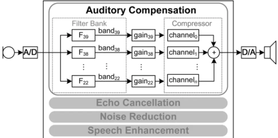
EARING AIDS [1] compensate the hearing loss with the auditory compensation algorithm and improve the speech intelligibility with the echo cancellation, the noise re-duction, and the speech enhancement algorithms. The block di-agram of an advanced digital hearing aid is illustrated in Fig. 1, which comprises the four mentioned function blocks. The audi-tory compensation algorithm makes up for the perceptual dis-tortion, such as the raised hearing thresholds and the squeezed hearing dynamic ranges, by performing the frequency-depen-dent and nonlinear amplification on the input sound. As shown Manuscript received January 12, 2009; revised May 28, 2009 and August 03, 2009; accepted August 27, 2009. Date of publication December 18, 2009; date of current version July 16, 2010. This work was supported in part by the Nation Science Council, Taiwan, under Grant NSC97-2220-E-009-021 and by a grant of making the chip in the National Chip Implementation Center (CIC), Taiwan. This paper was recommended by Associate Editor Y. Lian.Y.-T. Kuo and C.-W. Liu are with the Department of Electronics Engi-neering, National Chiao Tung University, Hsinchu, Taiwan 300. (e-mail: [email protected]).
T.-J. Lin was with the Department of Electronics Engineering, National Chiao Tung University, Hsinchu, Taiwan. He is now with the Microelectronics and In-formation Systems Research Center, National Chiao Tung University, Hsinchu 300, Taiwan 300.
Y.-T. Li was with the Department of Electronics Engineering, National Chiao Tung University, Hsinchu, Taiwan. He is now with MediaTek Inc., Hsinchu, Taiwan 300.
Digital Object Identifier 10.1109/TCSI.2009.2033539
in Fig. 1, the filter bank decomposes the input signal into dif-ferent bands so that the prescribed insertion gains can be applied to compensate the raised hearing thresholds. Then, the com-pressor is applied to reduce the signal’s dynamic range for fitting the output sound into the diminished and limited hearing range of the hearing-impaired person. Since the degree of hearing loss varies a lot for different frequencies, the multi-channel com-pressor, as shown in Fig. 1, is recommended. Modern hearing aids typically have a filter bank with more than 16 bands and a dynamic range compressor with three or four channels.
The auditory compensation, especially the filter bank, is the most important, but power-hungry, function in digital hearing aids because it makes the sound audible for hearing-impaired people. To the best of our knowledge, designing the filter bank for the hearing instruments in the literature can be classified into two categories: uniform filter banks [2], [3] and nonuni-form filter banks [4]–[9]. A 32-band discrete Fourier transnonuni-form (DFT) filter bank is designed in [2], whereas an 8-band filter bank with equal bandwidth finite-impulse response (FIR) fil-ters is implemented in [3]. The main drawback of the uniform filter banks is that they would need more computation complex-ities to meet the non-uniform frequency resolution requirement of human hearing system. Consequently, the nonuniform filter banks, which can go a step further to be classified into octave-band [4]–[6], critical-octave-band [7], and 1/3-octave-octave-band [8]–[10] filter banks, are more suitable.
A 7-band octave filter bank has been designed in [4] and [5], respectively, by using the interpolated FIR (IFIR) filter techniques. On the other hand, Lian and Wei [6] proposed an 8-band octave filter bank with the IFIR and frequency-re-sponse masking (FRM) techniques to reduce the computational complexity. In general, the 8-band filter bank can make good compensation for typical presbycusis hearing loss, whose characteristic is flatter. But more and more people have the noise-induced hearing losses, which may have great losses in some narrow frequency ranges. This kind of hearing losses needs more bands to compensate. A 16-band critical-like filter bank is designed in [7]. The critical bands match the human hearing perception; however, the irregular property of the crit-ical bands makes implementation difficult. The design in [7], for example, develops the 16 critical bands by applying 110-tap FIR filters, which have the significant computation complexity. Even though the critical-band filter bank is good for hearing aids, the desired filter bank should be designed such that each insertion gain obtained by hearing aid prescription formulas can be applied on it accordingly. The well-known hearing aid prescription formula, NAL-NL1 [11], for example, prescribes its insertion gains on 1/3-octave frequencies defined by ANSI S1.11 standard [10]; for Chinese, Chang et al.[12] have de-signed a Mandarin-specific hearing aid prescription formula, 1549-8328/$26.00 © 2010 IEEE
KUO et al.: DESIGN AND IMPLEMENTATION OF LOW-POWER ANSI S1.11 FILTER BANK FOR DIGITAL HEARING AIDS 1685
Fig. 1. Functional block diagram of the advanced hearing aid.
which prescribes gains also on the ANSI S1.11 1/3-octave fre-quencies. Consequently, the design of ANSI S1.11 filter bank will be necessary for the auditory compensation algorithms that are based on these hearing aid prescription formulas.
Most existing ANSI S1.11 filter banks are implemented by infinite-impulse response (IIR) filters [8], [9]. Indeed, the re-searches in psychoacoustics had shown that human ear is not sensitive to phase-distortion. The filter bank with IIR filters may be a good design with low computation complexity; however, FIR filters are still preferred and adopted in [3]–[7], not only for their linear phase but also for the stability and regular struc-ture. The round-off error of FIR filters is easier to analyze and control, which allows designers use simpler hardware [13], [14]. Although normal human ears are not sensitive to phase-delay, to design the filter bank of the auditory compensation with exact linear phase still has some advantages regarding the develop-ment of advanced hearing aids, which not only target at pro-cessing speech but also music signals. It has been shown that lis-teners are sensitive to phase relationships, particularly for tones of low frequency and rich harmonic structure, and hence, the phase has important effects on the perception of music signals [15]. Furthermore, the linear-phase property can make the pro-cessed sound more similar to the sound that users were used to. This could improve the speech intelligibility. In addition, preserving the phase cues helps the bilateral hearing aid users’ sound localization ability [16] and is also important for acoustic cancellation algorithms [7].
Recently, an efficient method for the design of FIR FRM fil-ters with reduced pass-band group delays is proposed in [17]. By incorporating the group delay constraint into the overall de-sign, where the group delay of the filter and its gradient are strongly related to filter coefficients, the optimum FRM filters with minimum pass-band group delay error can be obtained [17]. Besides, a straightforward approach to design FIR filters with piecewise-polynomial impulse responses is proposed in [18]. Compared to IFIR filter designs, the algorithm would have slightly less computation complexity for some cases. But the hardware cost and computation complexity increase greatly if the polynomial degree is higher than four [18]. Besides, due to the complicated design procedures of these two FIR filter design method, it is difficult to apply them for designing a low-com-plexity ANSI S1.11 filter bank. In order to reduce the power and
overall hardware cost of the ANSI S1.11 1/3-octave filter bank, a multi-stage, multirate FIR filter bank design is proposed [19]. In this paper, not only the algorithm development but also the architecture design as well as the silicon implementation of the ultra-low power ANSI S1.11 1/3-octave filter bank is present. Several low-power VLSI techniques are evaluated ex-haustively and then applied on our design. The proposed filter bank has been fabricated in TSMC 0.13- m CMOS technology and the test chip consumes only 87 W, which shows that the proposed design is more energy-efficient than other filter banks for hearing aids in the literature. The rest of this paper is orga-nized as follows. For readers’ reference, the ANSI S1.11 stan-dard will be briefly introduced in Section II. Section III demon-strates the proposed multirate algorithm for the efficient de-sign of ANSI S1.11 1/3-octave filter bank. Then, Section IV presents a systematic design flow for determining the filter co-efficients with minimized filter orders to meet the ANSI S1.11 standard. The hardware architecture and several applicable low-power VLSI techniques are considered in Section V. Finally, Section VI summaries the silicon implementation results and, some concluding remarks can be found in Section VII.
II. ANSI S1.11 STANDARD
The ANSI S1.11 standard [10] defines 43 1/3-octave bands covering the frequency range of 0–20 kHz. Each 1/3-octave band is specified by its mid-band frequency (or central fre-quency) and the bandwidth . The mid-band frequency of the
th band, denoted by , is defined by
(1) where , the reference frequency, is set to 1 kHz. For example, the mid-band frequency of the 22nd 1/3-octave band is 157 Hz and, the mid-band frequency of the 39th band is 8 kHz. With the mid-band frequency , two band-edge frequencies and of the th band are determined by
Fig. 2. ANSI S1.11 class-2 filter specification [10].
In the ANSI S1.11 standard, three classes of filters are described, i.e., class-0, class-1, and class-2. For each class of filters, some parameters regarding performance requirements are concerned, which include the relative attenuation, the linear operating range, the environment sensitivities (e.g., humidity and temperature), the maximum output signal, the terminating impedance, and so on. Fig. 2 illustrates the ANSI S1.11 class-2 filter specification on the th 1/3-octave band, where and denote the limits on the minimum and maximum attenuations of the th band filter, respectively. As shown in Fig. 2, the passband ripple is allowed to be less than or equal to 1 dB, while the filter should have at least 60dB attenuation at
frequencies smaller than and at frequencies
greater than . The relative attenuation is an
important design parameter from the hardware implementation point of view, because it strongly relates to the filter order.
Before leaving this section, we note that the specifications in either class-0 or class-1 filters are stricter than that of class-2 filters. However, the ANSI S1.11 class-2 1/3-octave band is chosen in our design because it has the comparable stopband attenuation requirement compared with other filter banks for hearing aids [3], [7]. On the other hand, the sampling rate is set to 24 kHz in order to provide the good sound quality.
III. MULTIRATEANSI S1.11 FILTERBANK
In this section, we present the complexity-effective design of an 18-band ANSI S1.11 filter bank, which implements the 22nd–39th 1/3-octave bands (denoted by ) for hearing aids. Fig. 3(a) illustrates the desired auditory compen-sation system based on this filter bank, in which the symbols and stand for the input and output sequences, respectively. The 18 bands cover six octaves, which are indexed by , and 6, starting from high frequencies toward low frequencies. With the filter bank, the input is first decomposed into 18 frequency-selected outputs, , as shown in Fig. 3(a). They are separately amplified by the pre-scribed insertion gains and then processed by the compressor. Finally, the outputs will be combined to form the output sequence .
For simplicity, if the filter , is ideal, then we have the following magnitude response
otherwise
Fig. 3. Derivation of the proposed multirate 18-band ANSI S1.11 1/3-octave filter bank for auditory compensation. (a) 18 parallel filters. (b) Multirate filter bank of 18 filters. (c) Reduced synthesis bank.
where and are the upper and lower band-edge fre-quencies of the th 1/3-octave band as described in Section II. According to the specification of ANSI S1.11 1/3-octave bands, we conclude that , the highest frequency in the 2nd oc-tave, is below when the sampling rate is set to 24 kHz. Since each 1/3-octave band in the 2nd octave is band-limited, we can down-sample the 2nd octave by 2 to reduce the com-putation complexity. Similarly, the highest frequency in
KUO et al.: DESIGN AND IMPLEMENTATION OF LOW-POWER ANSI S1.11 FILTER BANK FOR DIGITAL HEARING AIDS 1687
Fig. 4. Illustrations of IFIR implementation and noble identity.
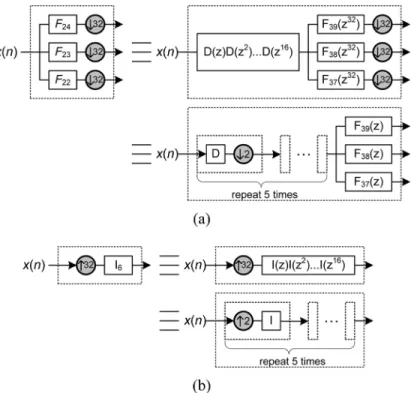
the 3rd octave is below , and so on. In other words, the bandwidth of the th octave only covers the frequencies below . Hence, the three 1/3-octave bands in the th octave can be down-sampled by , as shown in Fig. 3(b). By the theory of multirate systems [20], a synthesis bank with up-sam-plers and interpolation filters are necessary for reconstructing the signals.
The interpolation filters, i.e., in Fig. 3(b), will filter out all imaging distortions due to up-sampling. Recall that the bandwidths of the three 1/3-octave bands in the th oc-tave cover frequencies below . This fact implies that their imaging distortions only appear at frequencies higher than . Then, an ideal low-pass filter , whose response is
otherwise (2)
can be applied to remove the imaging distortions after up-sam-pling. Consequently, one can simplify the synthesis bank in Fig. 3(b) by replacing the three interpolation filters in the th octave with an ideal low-pass filter , as shown in Fig. 3(c). The multirate filter bank in Fig. 3(c) saves computations by re-ducing the sampling rates on the band-limited bands.
Now, let’s consider the 18 1/3-octave filters, i.e., – , in which , and are very narrow-band filters. For reducing the computation complexity, the interpolated FIR filter technique is applied in the following. Assume that the filter is an ideal low-pass filter with the response
otherwise. (3)
Hereafter, the -transform is used for convenience. From (1) and (3), we have
(4)
Then, by applying (4) iteratively, the filter can be deter-mined by
(5) Similarly, assuming the filter to be an ideal low-pass filter with the same response in (3), we can implement the filters
in (2) by cascading the filter . That is,
(6) Consequently, with (5) and (6), by the IFIR techniques and the noble identity [20], we can implement the filters – and
– in Fig. 3(c) with filters , and , as
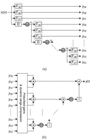
demon-strated in Fig. 4. Moreover, we can restructure the filter bank in Fig. 3(c) to a complexity-effective multirate filter bank, which is displayed in Fig. 5. To be brief, the proposed filter bank com-prises an analysis bank and a synthesis bank, where the former contains filters , and the decimation filter , while the latter contains the interpolation filter . With the developed multirate filter bank architecture, the hardware complexity is greatly reduced because we do not suffer from implementing those narrow-band filters, i.e., , and .
IV. DESIGN& OPTIMIZATION OFFILTERCOEFFICIENTS To realize the multirate filter bank in Fig. 5, the orders of
filters , and should be determined as small
as possible for reducing the computation complexity. Here we use to denote the frequency response of the desired th
Fig. 5. 18-band multirate auditory compensation system. (a) Analysis bank. (b) Dynamic range compressor and synthesis bank.
class-2 ANSI S1.11 1/3-octave band. To meet the specification, as shown in Fig. 2, the filter design constraint is
for
For simplicity, we apply the Parks-McClellan algorithm [21] to design the coefficients of FIR filters.
Due to the complicated multirate structure, it is difficult to de-sign these filters’ coefficients at the same time indeed. The most arduous part is how to determine the filters’ passband ripple, since both filters and as well as filters , and would influence the 18 bands’ frequency responses with each other.
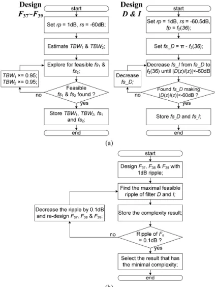
An efficient 2-step filter coefficient design flow, which is out-lined in Fig. 6, is proposed to design and optimize the filter co-efficients. In the first step, as shown in Fig. 6(a), we consider the design of filters , and as well as the design of filters and independently. That is, when designing filters , and , we assume filters and are Y_{36}ideal, and vice versa. The proposed algorithm explores the feasible solutions to make the filter orders as low as possible. After that, the determi-nation of the filters’ passband ripples will be considered in the second step, i.e., Fig. 6(b). Each filter’s ripple has to be refined and adjusted to make all 18 bands’ frequency responses meet the ANSI S1.11 specification. The following details each step of the proposed algorithm.
A. Step1a: Design , and
Consider the design parameters , and
, respectively, of the band-pass filter, as defined in Fig. 7(a).
According to the ANSI S1.11 specification, we set
dB and dB. Then, we need to find the values of
, and for filter , and ,
respec-tively, which however, cannot be straightforwardly derived because the ANSI S1.11 standard also describes the required attenuation in the transition regions (i.e.,
and ). Instead, we consider the following two
transition bandwidths, defined by and
for each filter , and .
The estimation of and of each band-pass
filter is conducted as follows. Note that to maximize (and ) as best as possible leads to minimizing the filter order thereof. For simplicity, we first decompose the ANSI S1.11 class-2 band-pass filter specification into the low-pass and high-pass specifications, respectively, as illustrated in Fig. 8. We then determine the value of by designing a high-pass filter satisfying the high-pass specification with the maximal transition bandwidth. Similarly, we find the value of by designing a low-pass filter satisfying the low-pass specification with the maximal transition bandwidth. Given
these estimated values of and , we then check
their feasibility. That is, we explore the possible values of and , respectively, to find out whether, with parameters
and , there exists feasible and that
make the designed band-pass filter meets the ANSI S1.11 specification. If the pair is not feasible, it will be decreased by 5% each time, i.e.,
until the designed band-pass filter meets the specification.
B. Step1b: Design D and I
Now, for filter and , let’s consider the design parameters and , respectively, of the low-pass filter, as defined in Fig. 7(b). According to the IFIR implementation shown
in Fig. 4(a), is implemented by cascading and
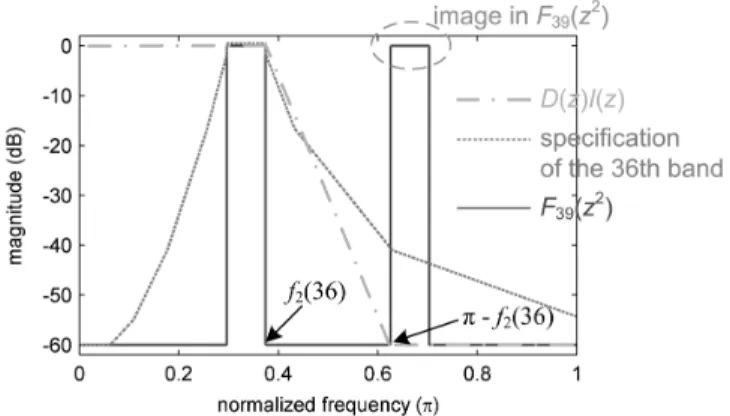
. So we should find a filter such that the response of satisfies the specification of the 36th band. Note that among the three bands in the second octave, here we only need to consider the 36th band because it would poses the strictest constraints on the filter . Besides, other octaves will automatically meet the specification if the second octave does, due to the octave-related bandwidth of this filter bank. Hence, if the 36th band meet the specification, the filter would also make – meet the specifications. Here we denote the passband and stopband frequencies of the filter as and respectively, and assume to be an ideal bandpass filter. Then we have the following constraints according to Fig. 9:
and (7)
Then, we consider 36th band’s output, . By the theory of multirate systems [20], we have
KUO et al.: DESIGN AND IMPLEMENTATION OF LOW-POWER ANSI S1.11 FILTER BANK FOR DIGITAL HEARING AIDS 1689
Fig. 6. Filter coefficient design flow. (a) Step 1: to designF –F and D&I independently. (b) Step 2: to fine-tune and to explore the optimal ripple distribution to jointly consider theF –F as well as D&I.
Hence, should be designed to suppress the distor-tion term, i.e., the second term of the right hand side of (8). Ac-cording to the ANSI S1.11 class-2 filter specification, we
con-clude that dB. On the other hand, the
de-sired term , i.e., the first term of the right
hand side of (8), is subjected to the specification of the 36th ANSI S1.11 class-2 band. Suppose that the passband frequency of the filter is denoted by , from the above discussion, we have following constraints:
and (9)
From (7) and (9), we can set the and to . But
we still need to explore the values of and to make dB.
We explore and ’s values with the flow shown in the right part of Fig. 6(a). The stopband attenuation, i.e., of the filters and , is first set to 60.5 dB, where the 0.5 dB is the design margin for compensating the influence of ’s passband ripple. And, we tentatively set the passband ripple, i.e., of these two filters, to 1 dB. Then, we now want to find the values of and , respectively. The values of
and should be small enough to make smaller
than dB. On the other hand, the values of and
should be as large as possible so that the orders of filters and are minimized. Therefore, we explore the values of and , repectively, by gradually decreasing their values from
until dB is satisfied, as depicted
in Fig. 6(a). The final result shows that and
, respectively.
C. Step2: Ripple Adjustment
In this step, we need to fine tune the passband ripples of filters , and , respectively, with the influences of filters and considered. As shown in Fig. 6(b), the ripple adjustment algorithm decreases the passband ripples of and from 1 to 0.1 dB with 0.1-dB stepping. Then, for each possible passband ripple, we explore how small the passband ripple of filters and should be to make all the 18 1/3-octave bands meet the ANSI S1.11 class-2 filter specification.
Table I summarizes the exploration results of the proposed algorithm. Generally speaking, the ripples of the filters and would decrease if that of the filters – increase. Neverthe-less, if the peaks of the ripples of the filters – are located at the positions where the filters and ’s ripples have valleys, these filters’ ripples would be cancelled by each other and the overall ripple would be reduced. That is why in some cases, as
Fig. 7. Input parameters rp; rs; fs1; fs2; fp1, and fp2 for designing: (a) band-pass and (b) low-pass filters.
Fig. 8. Illustration of dividing the band-pass filter specification in Fig. 2 into the low-pass and high-pass filter specifications, respectively.
shown in Table I, both the ripples of filters and that of filters and increase (e.g., 0.4 dB for , while 0.3 dB for & ).
We conclude from Table I that the optimal tap-lengths of filters , and are 41, 33, 26, 35, and 41, respec-tively. However, for saving the hardware complexity further, it is desirable that the tap-lengths of filters ,
Fig. 9. Suppression of the imaging distortion in the 36th band.
TABLE I
EXPLORATION FOROPTIMALRIPPLEDISTRIBUTION
and are all odd (or all even) so that these filters’ delay-lines can be shared. For this purpose, we redesign with only odd tap-lengths allowed. Then, the tap-lengths of filters , and are 41, 33, 27, 35, and 41, respectively, in our design.
V. LOW-POWERVLSI IMPLEMENTATION
This section considers the low-power VLSI implementation of the proposed multirate 18-band ANSI S1.11 1/3-octave filter bank. Here we only consider the analysis bank, since some ap-plications, such as audiometers or acoustic analyzers, do not need the synthesis bank. Moreover, in the hearing aid SoC, the synthesis bank will likely be merged with the dynamic range compressors for further optimization.
A. Folded Filter Bank Architecture
The proposed ANSI S1.11 1/3-octave filter bank contains six octaves and each octave is based on the identical set of filters , and , as illustrated in Fig. 5(a). For an area-ef-ficient implementation, it is nature to fold these six octaves, as demonstrated in Fig. 10; however, this incurs the scheduling problem. A good scheduling algorithm should avoid computa-tion conflicts (or stalls) and minimize the required storage ele-ments. In this paper, the recursive pyramid algorithm (RPA) [22] is considered. Suppose that each sampling period is divided into two time slots. Then, by RPA, the first octave is calculated every other slot, the second octave is calculated every four slots, the third every eight slots, and so on. Table II lists the computation
KUO et al.: DESIGN AND IMPLEMENTATION OF LOW-POWER ANSI S1.11 FILTER BANK FOR DIGITAL HEARING AIDS 1691
Fig. 10. Area-efficient filter bank with recursive structure [19].
TABLE II RPA SCHEDULING
scheduling of the folded multirate filter bank, in which the vari-ables and are the output of the th band and input of the th octave, respectively, as illustrated in Fig. 5(a). With RPA scheduling, only storage elements are required, where is the number of octaves and is the number of filter taps. (Note that and , respectively, in our design.)
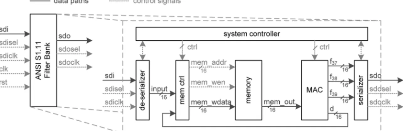
Based on the RPA scheduling, we design the proposed filter bank chip with the hardware block diagram shown in Fig. 11, in which the chip is consisting of modules of the system con-troller, the memory controller , the memory block, the multiply-and-accumulate (MAC) unit, the serializer, and the de-serializer. This chip is designed to operate at the 24-kHz sam-pling rate with 16-bit wordlength. Besides, in addition to the reset and clock signals (i.e., rst, and clk), there are 3-wire serial interfaces for input signals, i.e., sdi, sdisel, and sdiclk, as well as for output, i.e., sdo, sdosel, and sdoclk, in order to reduce the total pin count. The sdi and sdo represent the serial data bits of the input and output samples, respectively. The sdisel (or sdosel) and sdiclk (or sdoclk) pins are the select and word synchronization signals, respectively. The functionality and be-havior of each module would be described in the following.
The system controller coordinates the data flow according to the RPA scheduling algorithm and handles the input and output interfacing. The memory block contains a read-only memory (i.e., the coefficient ROM) that stores the coefficients of filters , and , respectively, as well as a random access memory (i.e., the data RAM) that maintains the delay-line data of the six octaves. Although each octave’s computation involves
four filters, these four filters can share a single delay-line since all of them have odd taps. Thus, only six delay-lines need to be implemented. Besides, since the longest filer’s tap-length is 41, the minimum size of the data RAM is 6 41 16 bits.
The input data of the data RAM may come from two sources: the external input sample and the output of the filter , as shown in Fig. 10. The former is written into the delay-line of the first octave at the beginning of each sampling period, while the latter is written into the delay-line of the th octave when the th octave’s computation is finished. The input data selection is handled by the memory controller, which also decodes the control signals from the system controller to generate appro-priate addresses, i.e., , and write enable signal, i.e.,
, for the memory block.
The datapath of the MAC unit is detailed in Fig. 12, which contains a multiplier, an adder, and a ‘tmp’ register together
with four accumulators, namely , and
, respectively. The MAC unit performs the FIR filtering computations of the four filters, i.e., , and , in an interleaved style. For instance, the computations of the th tap of these four filters are carried out as follows. One delay-line element is first read out from the data RAM and stored in the tmp register. Then, in order to exploit the coefficient symmetry property of linear phase FIR filters, another delay-line element is read out and accumulated into the one stored in the tmp reg-ister. During the third to the sixth cycles, the th coefficients of the four filters are consecutively read out from the coefficient ROM. They are then multiplied with the value stored in the tmp register and the results are, respectively, accumulated into the
corresponding accumulator registers: ,
and . Hence, after performing the computations of each
tap, the four accumulators, , and
would contain the outputs of the filters and ,
respectively.
Note that each tap’s computation requires 6 cycles. And, since the longest tap-length of the filter is 41, as indicated in Section IV.C, there are at most 21 coefficients need to be multiplied through the filtering operations. Consequently, the proposed architecture requires 126 cycles for each octave’s computation. On the other hand, two octaves’ computations will be scheduled in each sampling period with the RPA sched-uling algorithm. The clock period can then be determined by dividing the sampling period by 253, which includes 252 cycles for two octaves’ computations and one more cycle for writing the external input samples into the data RAM. The timing constraint of the chip is thus equal to 163 ns and a 6.13 MHz clock is used.
B. Low-Power Optimizations
The power consumption is indeed a critical issue for hearing aids. In this subsection, we investigate the low-power design techniques, available in the literature, for digital circuits.
1) Selective Coefficient Negation: The selective coefficient
negation technique [23] is intended to reduce the power of the multiplier in the MAC unit by minimizing its switching activity, which is directly affected by the Hamming distance of the two successive inputs. Because the MAC operation can be either
im-plemented as or , where we
Fig. 11. Hardware architecture of the proposed filter bank chip.
Fig. 12. Datapath of the MAC unit.
respectively, one can selectively negate the input to have the chance of reducing the Hamming distance of the data at input . However, this requires the MAC unit being able to perform the multiply-and-subtract operations. For each coefficient, says , either or will need to be stored in the coefficient memory, depending on which value would cause the smaller Hamming distance. The overhead is one additional bit associated with each coefficient, indicating that the coefficient is negated or not.
2) Computation Reordering: In the FIR filtering
computa-tion, we can exploit the commutative and associate properties of the summation operation to reorder the computation of the coefficient products. Thus, it is possible to reduce the Hamming distance in the multiplier’s inputs through exploring the design space of the accumulation orders [23]. Besides, in our design, we can further investigate the computation order with which the four filters , and are calculated in an interleaved style. However, because allowing the coefficient products being accumulated in arbitrary orders may make the system control and address generation complicated. In this paper, only the order in which the four filters are interleaved is explored to minimize the Hamming distance in the multiplier’s inputs.
3) Clock Gating: Considering the datapath of the MAC unit in Fig. 12, we can see that the four
accumu-lators, , and , totally have
bits. These accumulator registers consume significant power indeed. Since the register dissipates power at each transition of the clock signal, it would waste power if its value needs not to be updated. Furthermore, in our design, the computations of the four filters are processed in an interleaved manner, so each accumulator will be updated every 6 cycles. Hence, we can ideally save the accumulators’ power by 83%
Fig. 13. Multi-V implementation for power reduction.
with the clock-gating technique. We note that the clock-gating technique can also reduce the power on the clock tree network [24].
4) Operand Isolation: The aforementioned optimizations
mainly try to reduce the power of the MAC unit. Here we describe the operand isolation technique [24], which is adopted in our design to save the power of the memory block. Recall that the data RAM and the coefficient ROM are exclusively accessed. That is, values stored in the former can be maintained unchanged when the latter is accessed, and vice versa. Hence, the operand isolation technique can be applied, so that the data RAM dissipates no power when the coefficient ROM is accessed, and vice versa.
5) Multi- Implementation: The last low-power
opti-mization technique applied on our design is using multi-implementation. As well known, to lower the supply voltage of the circuit naturally improves the power performance, since the dynamic power dissipation of the CMOS circuit is directly pro-portional to the square of the power supply voltage. Recently, different blocks having different voltage supplies have been integrated in SoC. High voltages can be applied to the circuits on timing critical paths to maintain system performance, while the rest of the chip runs in the lower voltage for saving power. However, this would increase power planning complexity and some voltage level shifters are necessary for the interface across different power domains.
Fig. 13 shows the multi- implementation of our design for further power reduction. Since the reliability of memory block severely degenerates when the supply voltage decreases, we still maintain the supply voltage for the memory block at the nominal value, while , for the other block as shown in Fig. 13, is decreased.
KUO et al.: DESIGN AND IMPLEMENTATION OF LOW-POWER ANSI S1.11 FILTER BANK FOR DIGITAL HEARING AIDS 1693
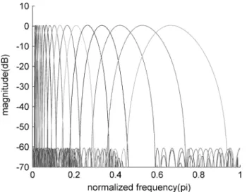
Fig. 14. Magnitude response of the proposed 18-band 1/3-octave filter bank.
VI. SILICONIMPLEMENTATIONRESULTS
A. Filter Response and Computation Complexity
The frequency response of the 18-band multirate FIR filter bank is shown in Fig. 14. For comparison purpose, we have also designed the following three ANSI S1.11 1/3-octave class-2 filter banks: (1) 18 parallel IIR Butterworth filters [12]; (2) the multirate filter bank with IIR Butterworth filters [8]; (3) 18 par-allel FIR filters. All filter coefficients are generated by using the MATLAB filter design toolbox (version 7.2). We note here that though Elliptic filters may have smaller orders than Butterworth filters, the difference can be neglected, since the orders of both filters are quite small. The 24-kHz sampling rate is sufficient to meet the Nyquist sampling theorem for the 22nd–39th ANSI S1.11 1/3-octave bands.
We have compared the frequency response of the narrowest band of the proposed multirate FIR filter bank with that of the other three filter banks [19]. Fig. 15 shows the magnitude re-sponses of the four filter banks’ bands, respectively. We note that all the four filter banks meet the ANSI S1.11 class-2 specification. Moreover, the FIR-based implementations of , as shown in Fig. 15(b) and (d), require a sharper slope in the transition region comparing that with IIR-based ones, as shown in Fig. 15(a) and (c). Because of the influences from decima-tion and interpoladecima-tion filters, the ripple of in Fig. 15(d) is slightly greater than that in Fig. 15(b). Besides, the image dis-tortions, the circled part in Fig. 15(c) and (d), are present in the responses of the two multirate filter banks.
Table III summarizes the numbers of multiplications and additions required for a single input sample being processed through the four filter banks. To meet the specifications of the ANSI S1.11 standard, in our simulation results, with the parallel structure, the FIR filter bank requires filters of order up to 1488, whereas the IIR filter bank requires only an 8-order Butterworth filter for as well as 6-order Butterworth filters for – . To sum up the computation complexity, the straightforward parallel FIR and IIR filter banks require totally 3270 and 192 multiplications, respectively (the coefficient symmetry is considered for FIR filters). On the other hand, the filters and in the proposed multirate FIR filter
Fig. 15. Frequency response of the designedF band in (a) parallel IIR bank, (b) parallel FIR bank, (c) multirate IIR bank, and (d) multirate FIR bank, respectively. The circled parts show the imaging distortion due to the multirate processing.
bank have tap-lengths of 41, 33, 27 and 35, respectively. They require only 21, 17, 14, and 18 multiplications. Besides, half of the outputs of filter are discarded due to the down-sampler. Averagely, the filter requires 9 multiplications. Therefore, each octave requires 61 multiplications. Moreover, the 2nd, 3rd, 4th, 5th, and 6th octaves’ sampling rates are only 1/2, 1/4, 1/8, 1/16, and 1/32 of that of the 1st octave; their computation complexity should be multiplied by 1/2, 1/4, 1/8, 1/16, and 1/32,
TABLE III
COMPUTATIONCOMPLEXITYCOMPARISONS OFFOURAUDITORY
COMPENSATIONSYSTEMS
TABLE IV
COMPARISONS OFSTORAGECOMPLEXITY
respectively. Hence the required multiplications per sample of our design is about 120 (note that the 6th octave doest not contain filter ). This saves about 96% computations of the parallel FIR filter bank. Even though the multirate approach also saves the computations of the IIR filter bank, the saving is not as significant as that in the FIR filter bank. Therefore, the proposed multirate FIR filter bank has comparable computation complexity compared with any IIR one.
We also make a comparison on the storage complexity for the proposed design and the filter banks presented in [6] and [7]. Table IV lists the requirement of delay elements of these filter banks. (Note that here we only consider the delay-lines but not the coefficient memory.) The filter bank in [7] uses a parallel architecture, so its delay-lines of each FIR filters can be shared. Even though it consists of 16 FIR filters with 110 taps, it only requires one delay-line with 110 storage elements. The filter bank in [6] uses the IFIR approach, which requires more delay elements. Although it implements two filters with only 19 and 39 taps respectively, the overall filter bank requires 668 delay elements. Finally, our design requires 246 delay elements as described in Section V-A. Note that the design in [7] uses a dual-port memory but our design uses a single-port one.
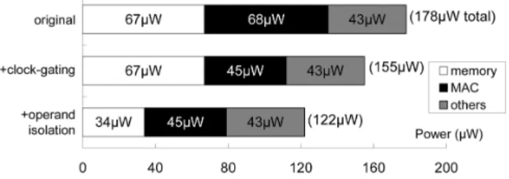
B. Effectiveness of Low-Power Optimizations
For evaluating the effectiveness of each low-power design technique described in Section V.B, we have implemented the proposed filter bank by using the cell-based design flow with the Artisan Metro standard cell library in TSMC 0.13 m tech-nology. The data RAM in the memory block is implemented with a 256 16 bit register file that is generated by Artisan’s Memory Compiler. In this subsection, the power is estimated through the gate-level and circuit-level simulations by using PrimePower and Nanosim, respectively. Three 250-ms input sequences are used for power estimation: the recorded female voice, male voice, and random signals.
As discussed in Section V-B, both the selective coefficient negation and the computation reordering techniques can apply
Fig. 16. Implementation results of applying low-power design techniques on our design.
to reduce the Hamming distance of the input pattern in order to minimize the switching activities of the MAC unit as best as possible to save power. Our simulations show that with the computation reordering, the averaged input Hamming distance is reduced from 6.4 to 5.3. After applying the selective nega-tion technique, the averaged Hamming distance can be further reduced to 3.6. That is, up to 43.75% Hamming distance of the input sequence to the MAC unit is diminished. Consequently, the low-power consumption of the MAC unit is guaranteed.
Now, let’s consider the operand isolation and clock-gating techniques on our design. The topmost bar in Fig. 16 shows the power distribution of the proposed filter bank, where the memory block consumes 67 W and the MAC unit consumes 68 W, respectively, and totally 178 W is dissipated. Applying the clock gating technique, the dissipated power of the MAC unit is reduced to 45 W, as shown in the second bar in Fig. 16. After further applying operand isolation on the memory block, the power of the memory block is saved by 33 W and the total power is reduced to 122 W, as depicted in the undermost bar in Fig. 16.
Finally, we consider the multi- implementation in the following. We first examine the multiplier, which is the main computing functional unit in the MAC unit. Fig. 17 depicts the simulation results of the energy per operation, in terms of pJ, as well as the critical-path delay, in terms of ns, of the multiplier re-lated to different supply voltages. The energy dissipation of the multiplier is lowered, as one expects; however, the critical-path delay increases with the decreasing of the supply voltage. Re-call that, as described in Section V.A, the timing constraint of the proposed architecture is moderate; this chip can operate at a lower supply voltage of 0.6 V without degrading performance. With multi- implementation, as indicated in Fig. 13, we set to 0.6 V, while maintain at 1.2 V. The cir-cuit-level simulation shows that the power consumption of the power domain is reduced to 53 W. Consequently, the proposed design consumes totally 87 W with the multi-implementation.
C. Silicon Implementation
Fig. 18 demonstrates the micro-photo of the test chip and the corresponding gate counts of different modules. The core area is 0.3 mm 0.3 mm (excluding I/O pads). The test chip contains two sets of the power/ground rings around the core. Besides, it has two power cuts on the chip’s right side, which is used to separate the power domains of and , respectively.
Table V summarizes the comparisons between the proposed design and other filter banks in the literature. Note that there is relatively less number of bands in [3] and [5], respectively.
KUO et al.: DESIGN AND IMPLEMENTATION OF LOW-POWER ANSI S1.11 FILTER BANK FOR DIGITAL HEARING AIDS 1695
Fig. 17. Energy dissipations and critical-path delays plot of the multiplier op-erated at different supply voltages.
Fig. 18. Silicon implementation.
Moreover, the filter bank in [5] only has 40 dB attenuation. The power performance of these filter banks may greatly increase if more bands are necessary and the attenuation is required to set to 60dB. On the other hand, the design in [7] is complicated, which implements each of the 16 bands with a 110-tap FIR filter. For the purpose of fair comparison with different process tech-nologies, we normalize the power with respect to the square of supply voltage [25], the process [25], as well as the number of filter bands, that is,
As shown in Table V, we conclude that the proposed multirate ANSI S1.11 1/3-octave filter bank is the most energy-efficient. Compared with other filter banks, our filter bank has the advan-tages of low computation complexity and compliance with the ANSI S1.11 1/3-octave specification. But, the price we pay is the long group delay, which is due to the multirate structure and the severe filter specification. The researches have shown that delays more than 10 ms may cause disturbing perception for hearing aid users listening to their own voices [26]. However, since the proposed iterative, multirate filter bank algorithm is regular and the designed architecture is quite modular, the pro-posed hardware design can then be easily modified so that the number of bands, which is equal to the number of iterations, is programmable. That is, the delay of the proposed filter bank can be reduced gradually if we can use fewer bands, for example, 10, 13, 16, or 18 bands. The programmable filter bank of the audi-tory compensation in the advanced hearing aids is helpful and is the adequate solution for hearing-impaired people. For example, in applications such as watching movies or listening to the radio and music, we can use all of the bands for higher quality, and
TABLE V
COMPARISONS OFFILTERBANKS FORHEARINGAIDS
in applications such as conversation, we can reduce the number of bands for shorter delay. Besides, the experimental results in [27] show that people having profounder hearing loss may be less sensitive to the delay effect. Therefore, if the users have se-vere hearing loss and are less sensitive to delay, they can use all the 18 bands to match the complicated prescriptions. On the contrary, if the users’ prescriptions are flatter, they can use fewer bands to match such prescriptions and thus reduce the hearing aids’ delay. Furthermore, the proposed filter bank not only ap-plies for hearing aids but also for some assistive listening de-vices. For example, some new cell phones are designed for the hearing impaired with built-in hearing loss compensator. And, the classroom broadcasting systems for children with hearing loss [28] also need the auditory compensation function. In these applications, the users would not hear their own voices through the instrument. So, the delay has less effect in these situations and the proposed filter bank is applicable.
VII. CONCLUSION
This paper addresses the low-power filter bank design for advanced digital hearing aids. In the literature, the standard ANSI S1.11 1/3-octave filter bank is rarely adopted in hearing aids due to high computation complexity even though it has the advantage of well matching the human hearing characteristics. We develop an efficient multirate filter bank algorithm to implement an 18-band ANSI S1.11 1/3-octave FIR filter bank. The proposed architecture needs only 4% of multiplications and additions of a straightforward parallel FIR filter bank design. We also investigate and apply several lower-power VLSI techniques, available in the literature, on our design. The clock gating and operand isolation saves a great amount of the power consumption. A test chip of this 18-band ANSI S1.11 1/3-octave filter bank has been fabricated in TSMC 0.13 m CMOS technology. The chip consumes only 87 W for the 18-band 24-kHz audio signal processing. The proposed filter bank is energy-efficient and being able to precisely matching the prescribed gains generated by the widely used NAL-NL1 hearing aid prescription formula. Although the group delay, which is the price paid for the low computation complexity, is long, our design is still very useful for some delay-insensitive applications.
ACKNOWLEDGMENT
This paper was extensively discussed in a series of meetings and extensive exchanges with Prof. S.-T. Young at the National Yang-Ming University, Taipei, Taiwan. The authors would like to thank Prof. Young for providing the Mandarin-specific hearing aid algorithm, the prescription formula, and a lot of constructive advice on this work.
REFERENCES
[1] H. Dillon, Hearing Aids. New York: Thieme Medical Publisher, 2001.
[2] R. Brennan and T. Schneider, “A flexible filter bank structure for ex-tensive signal manipulations in digital hearing aids,” in Proc. IEEE Int.
Symp. Circuits Syst., CA, 1998, pp. 569–572.
[3] H. Li, G. A. Jullien, V. S. Dimitrov, M. Ahmadi, and W. Miller, “A 2-digit multidimensional logarithmic number system filter bank for a digital hearing aid architecture,” in Proc. IEEE Int. Symp. Circuits Syst., AZ, 2002, pp. II-760–763.
[4] T. Lunner and J. Hellgren, “A digital filterbank hearing aid—Design, implementation and evaluation,” in Proc. ICASSP Conf., 1991, pp. 3661–3664.
[5] L. S. Nielsen and J. Sparso, “Designing asynchronous circuits for low power: An IFIR filter bank for a digital hearing aid,” in Proc. IEEE, Feb. 1999, vol. 87, no. 2, pp. 268–281.
[6] Y. Lian and Y. Wei, “A computationally efficient nonuniform FIR dig-ital filter bank for hearing aids,” IEEE Tran. Circuits Syst., vol. 52, no. 12, pp. 2754–2762, Dec. 2005.
[7] K. S. Chong, B. H. Gwee, and J. S. Chang, “A 16-channel low-power nonuniform spaced filter bank core for digital hearing aid,” IEEE Tran.
Circuits Syst., vol. 53, no. 9, pp. 853–857, Sep. 2006.
[8] A. Lozano and A. Carlosena, “DSP-based implementation of an ANSI S1.11 acoustic analyzer,” IEEE Trans. Instrum. Meas., vol. 52, no. 4, pp. 1213–1219, Aug. 2003.
[9] S. B. Davis, “Octave and fractional octave band digital filtering based on the proposed ANSI standard,” in Proc. ICASSP Conf., 1986, pp. 945–948.
[10] Specification for Octave-Band and Fractional-Octave-Band Analog
and Digital Filters, ANSI Standard S1.11-2004.
[11] D. Byrne, H. Dillon, T. Ching, R. Katsch, and G. Keidser, “NAL-NL1 procedure for fitting nonlinear hearing aids: Characteristics and com-parisons with other procedures,” J. Amer. Acad. of Audiology, vol. 12, no. 1, pp. 37–54, Jan. 2001.
[12] J. H. Chang, K. S. Tsai, P. C. Li, and S. T. Young, “Computer-aided simulation of multi-channel WDRC hearing aids,” in Proc. 17th Annu.
Conv. & Expo Amer. Acad. of Audiology, 2005.
[13] E. Ozalevli, W. Huang, P. E. Hasler, and D. V. Anderson, “A recon-figurable mixed-signal VLSI implementation of distributed arithmetic used for finite-impulse response filtering,” IEEE Tran. Circuits Syst. I:
Reg. Papers, vol. 55, no. 2, pp. 510–521, Mar. 2008.
[14] M. Aktan, A. Yurdakul, and G. Dundar, “An algorithm for the design of low-power hardware-efficient FIR filters,” IEEE Tran. Circuits Syst.
I: Reg. Papers, vol. 55, no. 6, pp. 1536–1545, Jul. 2008.
[15] M. Chasm and F. A. Russo, “Hearing aids and music,” Trends in
Am-plification, vol. 8, no. 2, pp. 35–47, 2004.
[16] T. Van den Bogaert, J. Wouters, T. J. Klasen, and M. Moone, “Dis-tortion of interaural time cues by directional noise reduction system in modern digital hearing aids,” in Proc. IEEE Workshop on Appl. of
Signal Process. to Audio and Acoust., 2005.
[17] Y. Z. Liu and Z. P. Lin, “Optimal design of frequency-response masking filters with reduced group delays,” IEEE Tran. Circuits Syst.
I: Reg. Papers, vol. 55, no. 6, pp. 1560–1570, Jul. 2008.
[18] R. Lehto, T. Saramaki, and O. Vainio, “Synthesis of narrowband linear-phase filters with a piecewise-polynomial impulse response,”
IEEE Tran. Circuits Syst. I: Reg. Papers, vol. 54, no. 10, pp.
2262–2276, Oct. 2007.
[19] Y. T. Kuo, T. J. Lin, Y. T. Li, W. H. Chang, and C.-W. Liu, “Design of ANSI S1.11 filter bank for digital hearing aids,” in Proc. ICECS Conf., 2007, pp. 242–245.
[20] P. P. Vaidyanathan, Multirate Systems and Filter Banks. , New Jersey: Prentice Hall, 1993.
[21] L. R. Rabiner and B. Gold, Theory and Application of Digital Signal
Processing. New York: Prentice Hall, 1975.
[22] M. Vishwanath, “The recursive pyramid algorithm for the discrete wavelet transform,” IEEE Trans. Signal Process., vol. 42, no. 3, pp. 673–676, Mar. 1994.
[23] M. Mehendale and S. D. Sherlekar, VLSI Synthesis of DSP
Ker-nels-Algorithmic and Architectural Transformations. Amsterdam, the Netherlands: Kluwer Academic, 2001.
[24] A. P. Chandrakasan and R. W. Brodersen, Low Power Digital CMOS
Design. Amsterdam, the Netherlands: Kluwer Academic, 1995.
[25] T. C. Chen and R. B. Sheen, “A power-efficient wide-range phase-locked loop,” IEEE J. Solid-State Circuits, vol. 37, no. 1, pp. 51–62, Jan. 2002.
[26] M. A. Stone and B. C. J. Moore, “Tolerable hearing-aid delays: III. effects on speech production and perception of across-frequency vari-ation in delay,” Ear and Hearing, vol. 24, no. 2, pp. 175–183, 2003. [27] M. A. Stone and B. C. J. Moore, “Tolerable hearing-aid delays: IV.
Effects on subjective disturbance during speech production by hearing-impaired subjects,” Ear and Hearing, vol. 26, no. 2, pp. 225–235, 2005. [28] D. E. Lewis, “Assistive Devices for classroom listening: FM systems,”
Amer. J. Audiology, vol. 3, pp. 70–83, 1994.
Yu-Ting Kuo received the B.S. and the M.S. degrees in electronics engineering from National Chiao Tung University, Taiwan, in 2004 and 2006, respectively. He is currently working towards the Ph.D. degree in electronics engineering at National Chiao Tung University, Taiwan.
His researches include low-power signal pro-cessing, digital hearing aids, and computer architecture.
Tay-Jyi Lin (S’00–M’06) received the B.S. degree in electrical and control engineering and the Ph.D. degree in electronics engineering, from National Chiao Tung University, Taiwan, in 1998 and 2005, respectively.
He is currently with the Microelectronics and Information Systems Research Center, National Chiao Tung University, as a researcher assistant professor. His research interests include VLSI signal processing, low-power design methodology, and computer architecture.
Yueh-Tai Li received the B.S. degree in electrical and control engineering and the M.S. degrees in elec-tronics engineering from National Chiao Tung Uni-versity, Taiwan, in 2006 and 2008, respectively.
He is currently with MediaTek, Inc. Taiwan.
Chih-Wei Liu (M’03) was born in Taiwan. He re-ceived the B.S. and Ph.D. degrees, both in electrical engineering, from National Tsing Hua University, Hsinchu, Taiwan, in 1991 and 1999, respectively.
From 1999 to 2000, he was an integrated circuits design engineer at the Electronics Research and Ser-vice Organization (ERSO) of Industrial Technology Research Institute (ITRI), Hsinchu, Taiwan. Then, near the end of 2000, he started to work for SoC Technology Center (STC) of ITRI as a project leader and eventually left ITRI at the end of Sept. 2003. He is currently with the Department of Electronics Engineering and the Institute of Electronics, National Chiao Tung University, Hsinchu, Taiwan, as an associate professor. His current research interests are SoC and VLSI system design, processor for embedded computing system, digital signal processing, digital communications, and coding theory.
![Fig. 2. ANSI S1.11 class-2 filter specification [10].](https://thumb-ap.123doks.com/thumbv2/9libinfo/7570862.125186/3.891.467.816.93.908/fig-ansi-s-class-filter-specification.webp)
![Fig. 10. Area-efficient filter bank with recursive structure [19].](https://thumb-ap.123doks.com/thumbv2/9libinfo/7570862.125186/8.891.124.365.99.239/fig-area-efficient-filter-bank-recursive-structure.webp)