In Ga N Ga N nanostripe grown on pattern sapphire by metal organic chemical vapor
deposition
T. S. Ko, T. C. Wang, R. C. Gao, Y. J. Lee, T. C. Lu, H. C. Kuo, S. C. Wang, and H. G. Chen
Citation: Applied Physics Letters 90, 013110 (2007); doi: 10.1063/1.2430487 View online: http://dx.doi.org/10.1063/1.2430487
View Table of Contents: http://scitation.aip.org/content/aip/journal/apl/90/1?ver=pdfcov
Published by the AIP Publishing
Articles you may be interested in
Correlating exciton localization with compositional fluctuations in In Ga N Ga N quantum wells grown on GaN planar surfaces and facets of GaN triangular prisms
J. Appl. Phys. 102, 093502 (2007); 10.1063/1.2802291
Radiative and nonradiative lifetimes in nonpolar m -plane In x Ga 1 x N Ga N multiple quantum wells grown on GaN templates prepared by lateral epitaxial overgrowth
J. Vac. Sci. Technol. B 25, 1524 (2007); 10.1116/1.2746354
Growth of InP self-assembled quantum dots on strained and strain-relaxed In x ( Al 0.6 Ga 0.4 ) 1 x P matrices by metal-organic chemical vapor deposition
J. Appl. Phys. 100, 043511 (2006); 10.1063/1.2244519
Superlattice-like stacking fault and phase separation of In x Ga 1x N grown on sapphire substrate by metalorganic chemical vapor deposition
Appl. Phys. Lett. 77, 247 (2000); 10.1063/1.126939
Phase separation and ordering coexisting in In x Ga 1x N grown by metal organic chemical vapor deposition
Appl. Phys. Lett. 75, 2202 (1999); 10.1063/1.124964
This article is copyrighted as indicated in the article. Reuse of AIP content is subject to the terms at: http://scitation.aip.org/termsconditions. Downloaded to IP: 140.113.38.11 On: Thu, 01 May 2014 01:16:39
InGaN / GaN nanostripe grown on pattern sapphire by metal organic
chemical vapor deposition
T. S. Ko, T. C. Wang, R. C. Gao, Y. J. Lee, T. C. Lu,a兲 H. C. Kuo,b兲 and S. C. Wang
Department of Photonics and Institute of Electro-Optical Engineering, National Chiao Tung University, 1001 Ta Hsueh Rd., Hsinchu 30050, Taiwan, Republic of China
H. G. Chen
Department of Materials Science and Engineering, I-Shou University, Kaohsiung 840, Taiwan, Republic of China
共Received 4 October 2006; accepted 5 December 2006; published online 4 January 2007兲 The authors have used metal organic chemical vapor deposition to grow InGaN / GaN multiple quantum well 共MQW兲 nanostripes on trapezoidally patterned c-plane sapphire substrates. Transmission electron microscopy共TEM兲 images clearly revealed that the MQWs grew not only on the top faces of the trapezoids but also on both lateral side facets along the关0001兴 direction defined by the selected area electron diffraction pattern. Meanwhile, dislocations that stretched from the interfaces between the GaN and the substrates did not pass through the MQWs in the TEM observation. Microphotoluminescence measurements verified that the luminescence efficiency from a single nanostripe was enhanced by up to fivefold relative to those of regular thin film MQW structures. Observation of the cathodoluminescence identified the areas of light emission and confirmed that enhanced emission occurred from the nanostripes. © 2007 American Institute of
Physics. 关DOI:10.1063/1.2430487兴
Group III nitride semiconductors attract much attention because of their applications in light emitting devices such as highly efficient light emitting diodes 共LEDs兲 and laser diodes.1,2Although such LEDs are commercially available, it is difficult to manufacture highly efficient LEDs because a great number of threading dislocation densities occur when group III nitride alloys are grown on c-plane sapphire.3 Moreover, most of the light emitted from the LED active region would remain trapped by the high refractive index of GaN as a result of total internal reflection at the interface between the LED and air.4,5 Recently, Kim et al. demon-strated high-efficiency LEDs from dislocation-free InGaN / GaN multiple quantum well共MQW兲 nanorod arrays prepared using a metal organic chemical vapor deposition 共MOCVD兲 system.6
Fujii et al. improved the luminescence efficiency of LEDs by roughening the sample surface to en-large the emission area.7Wang et al. fabricated a micropillar InGaN / Cu LED combining a patterned sapphire substrate.8 From these previous studies, it is clearly most desirable to grow InGaN / GaN heterostructures that have low dislocation densities and large surface areas in order to increase the emission efficiency. Nanostructure devices could play an im-portant role in overcoming the existing dislocations and dif-ficulties encountered in light extraction. In this letter, we describe high-efficiency InGaN / GaN MQWs embedded in nanostripe structures prepared through MOCVD growth on
c-plane sapphire substrates patterned with trapezoid stripes.
The structural analysis of these materials is discussed in terms of their crystal orientations关observed using scanning electron microscopy 共SEM兲 and transmission electron mi-croscopy共TEM兲兴; the optical characteristics were measured using a microphotoluminescence共-PL兲 system. The
lumi-nescence efficiency 共measured using the -PL兲 and the cathodoluminescence of a single nanostripe were greatly en-hanced in comparison to those of conventional thin film MQW structures. In addition, the MQWs embedded in the nanostripe structures were free of dislocations resulting from the interface between the GaN and the substrate, as observed from TEM images.
All samples were grown through MOCVD in a single-wafer Emcore system with a vertical reactor design. We used SiO2stripes oriented along the关11¯00兴 direction as an etching
mask to define patterns lithographically on a sapphire sub-strate. The dimensions of the mask openings and periods were 6 and 8m, respectively. The sample was wet etched using a H3PO4 base solution at 300 ° C for 30 min.
After-ward, the sample was dipped into a buffered oxide etch 共NH4F : HF, 6:1兲 solution to remove the SiO2 layers for the
following epitaxial growth. The growth parameters of the conventional light-emitting diode on the c plane were used for the epitaxial step, including a 30 nm GaN buffer layer, 1m bulk GaN layer, three pairs of MQWs with 6 nm In0.2Ga0.8N wells and 16 nm GaN barriers, and a 100 nm
GaN capping layer. The surface morphology and microstruc-ture of the as-grown sample were observed using SEM and TEM. A-PL system pumped by a He–Cd laser was used to study the luminescence in the structure, with the spatial reso-lution estimated to be approximately 0.7m. The spatially resolved cathodoluminescence共CL兲 imaging data were ob-tained by scanning the SEM over various parts of the samples.
Figure 1共a兲 provides a schematic diagram of the as-grown sample. For the trapezoidally patterned sapphire, the top width, bottom width, and depth were approximately 450 nm, 6.7m, and 4m, respectively. Figure 1共b兲 dis-plays a top-view SEM image of the as-grown sample. Nanostripes had grown on the top base of the trapezoid.
a兲Electronic mail: [email protected] b兲Electronic mail: [email protected]
APPLIED PHYSICS LETTERS 90, 013110共2007兲
0003-6951/2007/90共1兲/013110/3/$23.00 90, 013110-1 © 2007 American Institute of Physics
This article is copyrighted as indicated in the article. Reuse of AIP content is subject to the terms at: http://scitation.aip.org/termsconditions. Downloaded to IP: 140.113.38.11 On: Thu, 01 May 2014 01:16:39
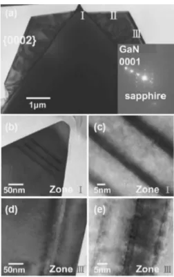
Many V defects and small pits were also widely distributed over the lateral side of the trapezoid. Figure2共a兲presents a typical cross-sectional bright-field TEM image, with differ-ent zones labeled I, II, and III. The nanostripe structures existed on top of the trapezoid pattern of the sapphire sub-strate in zone I. In the TEM images, the MQW structures appeared only in zones I and III. No MQW structures were detected from TEM observation of zone II, indicating that the growth direction might occur only toward the top and lateral facets of the trapezoidally patterned sapphire. Accord-ing to the diffraction pattern, the GaN layer grown epitaxi-ally on the top face of the trapezoid followed typical 兵0001其GaN 储兵0001其sapphireand关112¯0兴GaN 储关1100兴sapphire
crystal-lographic relationships, as presented in the inset to Fig.2共a兲. The crystallographic relationship of the side facets of the trapezoid differed from that of a typical c-plane hexagonal crystallographic geometry, although the crystallographic fac-ets in zone III belonged to the c plane. The exact determina-tion of the crystallographic reladetermina-tionship between the GaN and the inclined sapphire face will require the analysis of more than one diffraction pattern from different zone axes; such a study is in progress. Figures 2共b兲–2共e兲reveal high-resolution TEM images of triple-MQW structures grown on zones I and III, respectively. The thickness of the MQW structure on zone I was larger than that on zone III probably because of the different gas streams caused by the striped patterns on the substrates. From the angle of inclination be-tween the top and side facets of the GaN grown on zone I in this nanostriped structure, we determined that the side facet
was a兵11¯02其 r plane. Moreover, the V-shaped defects com-monly observed under conditions of kinetically limited growth of c-plane GaN and its alloys9 are visible in the bottom-left-hand region of the TEM image in Fig.2共a兲.
A room temperature -PL system equipped with a He–Cd laser was used to study the luminescence of the struc-ture. We obtained PL spectra by focusing the laser beam on zones I and III关as labeled in Fig.2共a兲兴. Figure3共a兲displays the-PL results obtained at the different zones of the struc-ture. The PL maximum at zone I appeared at approximately 460 nm, a longer wavelength than that of zone III. According to the TEM images in Figs.2共b兲and2共d兲, the widths of the wells were approximately 6 and 2.5 nm for zones I and III, respectively. The longer emission wavelength at zone I rela-tive to that at zone III was due to the wider quantum well size having a weaker quantum confinement effect. In addi-tion, the PL intensity from the single nanostripe in zone I was enhanced up to almost fivefold relative to that of zone III and even relative to that of the regular equal pairs of MQWs in the conventional thin film structures. The much-improved emission efficiency might have arisen from en-hanced light extraction efficiency and/or internal quantum efficiency. Because the MQWs were embedded in the trap-ezoidal nanostripe structure, the inclination of the large-area emission surface greatly enhanced the light extraction effi-ciency in comparison with those of conventional flat MQW thin films, where the light emitted only within the cone de-fined by the angle of total internal reflection. We have used TEM to observe the root of the nanostripe structure in zone II. Figure3共b兲 displays the distribution of edge dislocations in a cross-sectional dark-field TEM image of the nanostripe structure. In general, edge dislocations often stretch through to the surface to become V defects. This image, however, FIG. 1. 共a兲 共Color兲 Schematic representation of the nanostripe MQWs
grown on trapezoidally patterned sapphire substrates.共b兲 Top-view SEM images of the as-grown sample.
FIG. 2. 共a兲 Cross-sectional TEM image of the trapezoidal structure. The crystalline orientation between the GaN and sapphire in zone II was defined by the diffraction pattern, as indicated in the inset.共b兲–共e兲 High-resolution TEM images共different magnifications兲 of the MQWs in zones I 关共b兲 and 共c兲兴 and III关共d兲 and 共e兲兴.
013110-2 Ko et al. Appl. Phys. Lett. 90, 013110共2007兲
This article is copyrighted as indicated in the article. Reuse of AIP content is subject to the terms at: http://scitation.aip.org/termsconditions. Downloaded to IP: 140.113.38.11 On: Thu, 01 May 2014 01:16:39
indicated that the edge dislocations were terminated in the growth of the bulk GaN layer below the MQW layers. As a result, the nanostripe structure helped to form MQWs that were free from edge dislocations and facilitated the enhance-ment of internal quantum efficiency.
Figures4共a兲and4共b兲 present spatially resolved cathod-oluminescence images recorded using optical filters at 365 and 460 nm, respectively, from above the sample at room temperature. In Fig.4, zones I and III are the same positions as those defined in Fig.2共a兲. The emissions 365 and 460 nm originated mainly from the contributions of the bulk GaN and the InGaN / GaN MQWs. In Fig.4共a兲, the optically acti-vated region reveals the locations of the bulk GaN, including some areas between the nanostripes and the top face of the trapezoids; in Fig. 4共b兲, however, the bright 460 nm MQW emission lines appear at the top of the trapezoids. Mean-while, zone II also exhibited the MQWs’ luminescence, con-firming the results of the TEM analysis in Fig. 2. We ob-serve, however, that the luminescence intensity from the MQWs on the nanostripe structures is stronger than those on both of the lateral regions. Because the distribution of de-fects and the quality of the crystal can both influence the CL intensity,10the high intensity of the emission from the nanos-tripe structure again suggests the good epitaxial quality—and lack of V defects—of the MQWs grown on the trapezoidally patterned sapphire substrates.
In summary, we have used MOCVD to fabricate InGaN / GaN MQWs nanostripes on trapezoidally patterned
sapphire substrates. A series of special relations and planes of crystallization were defined by diffraction pattern analysis and TEM observations. The results of-PL and CL experi-ments indicate that the intensity of the luminescence from the MQWs embedded in the nanostripe structure was en-hanced up to fivefold relative to those of regular thin film MQWs, probably as a result of much-improved internal and external quantum efficiencies. Therefore, these MQW nanos-tripe arrays are capable of enhancing luminescence and ap-pear to be suitable for application to the fabrication of high-efficiency light-emitting devices.
The authors would like to thank Professor Y. F. Chen of National Taiwan University for CL support. The study was supported by the MOE ATU program and, in part, by the National Science Council of the Republic of China under Contract Nos. NSC 95-2120-M-009-008, NSC 95-2752-E-009-007-PAE, and NSC 95-2221-E-009-282.
1S. Nakamura, Science 281, 956共1998兲.
2H. Morkoç, S. Strite, G. B. Gao, M. E. Lin, B. Sverdlov, and M. Burns, J.
Appl. Phys. 76, 1363共1994兲.
3F. A. Ponce and D. P. Bour, Nature共London兲 386, 351 共1997兲. 4C. Huh, K. S. Lee, E. J. Kang, and S. J. Park, J. Appl. Phys. 93, 9383
共2003兲.
5I. Schnitzer, E. Yablonovitch, C. Caneau, T. J. Gmitter, and A. Scherer,
Appl. Phys. Lett. 63, 2174共1993兲.
6H. M. Kim, Y. H. Cho, H. Lee, S. I. Kim, S. R. Ryu, D. Y. Kim, T. W.
Kang, and K. S. Chung, Nano Lett. 4, 1059共2004兲.
7T. Fujii, Y. Gao, R. Sharma, E. L. Hu, S. P. DenBaars, and S. Nakamura,
Appl. Phys. Lett. 84, 855共2005兲.
8W. K. Wang, S. Y. Huang, K. S. Wen, D. S. Wuu, and R. H. Horng, Appl.
Phys. Lett. 88, 181113共2006兲.
9X. Wu, C. Elsass, A. Abare, M. Mack, S. Keller, P. Petroff, S. Denbaars,
J. Speck, and S. Rosner, Appl. Phys. Lett. 72, 692共1998兲.
10B. A. Haskell, T. J. Baker, M. B. McLaurin, F. Wu, P. T. Fini, S. P.
DenBaars, J. S. Speck, and S. Nakamura, Appl. Phys. Lett. 86, 111917 共2005兲.
FIG. 3.共Color online兲 共a兲 PL spectra recorded at zones I and II and that of a conventional thin film with three pairs of MQWs.共b兲 Cross-sectional dark-field TEM images of the nanostripes.
FIG. 4. Monochromatic top view CL images: 共a兲 =365 nm and 共b兲 =460 nm.
013110-3 Ko et al. Appl. Phys. Lett. 90, 013110共2007兲
This article is copyrighted as indicated in the article. Reuse of AIP content is subject to the terms at: http://scitation.aip.org/termsconditions. Downloaded to IP: 140.113.38.11 On: Thu, 01 May 2014 01:16:39