Influence of thermal annealing on the electron emission of InAs quantum dots
containing a misfit defect state
J. F. Chen, C. H. Yang, R. M. Hsu, and U. S. Wang
Citation: Journal of Applied Physics 105, 063705 (2009); doi: 10.1063/1.3081654 View online: http://dx.doi.org/10.1063/1.3081654
View Table of Contents: http://scitation.aip.org/content/aip/journal/jap/105/6?ver=pdfcov Published by the AIP Publishing
Articles you may be interested in
Presentation and experimental validation of a model for the effect of thermal annealing on the photoluminescence of self-assembled InAs/GaAs quantum dots
J. Appl. Phys. 107, 123107 (2010); 10.1063/1.3431388
Annealing of self-assembled InAs/GaAs quantum dots: A stabilizing effect of beryllium doping Appl. Phys. Lett. 94, 072105 (2009); 10.1063/1.3086298
Effects of alloy intermixing on the lateral confinement potential in In As Ga As self-assembled quantum dots probed by intersublevel absorption spectroscopy
Appl. Phys. Lett. 90, 163107 (2007); 10.1063/1.2724893
Effect of incorporating an InAlAs layer on electron emission in self-assembled InAs quantum dots J. Appl. Phys. 99, 014303 (2006); 10.1063/1.2150258
Widely tunable intersubband energy spacing of self-assembled InAs/GaAs quantum dots due to interface intermixing
J. Appl. Phys. 86, 2687 (1999); 10.1063/1.371111
meV after annealing at 650 and 700 ° C for 1 min, respectively. This emission energy reduction is correlated with the photoluminescence blueshift which is attributed to the interdiffusion of atoms across the QD interface. The electron emission from the QD first excited and ground states is found to be a thermal emission at high temperatures and a tunneling emission at low temperatures. The tunneling energy barrier is found to be comparable to the thermal emission energy, supporting a thermal emission to the GaAs conduction band. This study illustrates a significant effect of a defect state on the electron-emission process in the QDs, suggesting the possibility of modifying the electron emission time of the QDs by purposely introducing a deep defect state. © 2009 American
Institute of Physics.关DOI:10.1063/1.3081654兴
I. INTRODUCTION
Transitions between the conduction-band共CB兲 states of InAs self-assembled quantum dots共QDs兲 共Refs.1–8兲 are in
the long-wavelength infrared region and referred to as intra-band transitions. Understanding the electron emission mechanism9–12is important for infrared applications such as photodetectors.13,14Kapteyn et al.9observed a two-step tron emission process: a thermal emission from the QD elec-tron ground state共EGS兲 to first excited state 共FES兲 and then tunneling to the GaAs CB, rather than a thermal emission from the QD EGS to the GaAs CB. This work and related studies10,11 suggest a significant tunneling emission for the electrons escaping from the QDs. Lowering the background concentration in the GaAs barrier layer is expected to in-crease the tunneling width and suppress the tunneling emis-sion. Another approach is to induce additional carrier deple-tion in the GaAs barrier layer by purposely introducing a deep defect state. Defect-free coherent QDs can be formed by partial strain relaxation. However, when InAs deposition thickness exceeds a critical thickness共⬃3 ML兲, strain is re-laxed by inducing lattice misfits.15,16With an InGaAs strain-reducing capping layer,17 the misfits are confined near the QD bottom interface and behave like electron-trapping cen-ters. These deep levels can cause additional carrier depletion and suppress the tunneling emission, leading to a significant modification of the electron emission process in the QDs. Postgrowth thermal annealing18–22 is expected to shift up-ward the QD electron states because a blueshift of photolu-minescence共PL兲 is usually observed due to the interdiffusion
of atoms across the QD interface. Thus, it would be interest-ing to study the effect of the thermal annealinterest-ing on the elec-tron emission from the QDs and compare the results with the PL spectra. In this work, the electron emission from relaxed InAs QDs, subjected to thermal annealing at different tem-peratures, are systematically investigated using capacitance-voltage共C-V兲 profiling and admittance spectroscopy. Due to the long emission time, the misfit-related defect state is probed by voltage-dependent deep-level-transient spectros-copy共DLTS兲.
II. EXPERIMENTS
The InAs QDs with an InGaAs capping layer were grown on n+-GaAs共100兲 substrates by solid source
molecu-lar beam epitaxy in a Riber machine. On top of a 0.3-m-thick Si-doped GaAs 关共6–10兲⫻1016 cm−3兴 barrier
layer, an InAs layer with different deposition thicknesses from 2 to 3.3 ML was deposited at 490 ° C共at a rate of 0.26 Å/s兲 to form the QDs. The DLTS and cross-sectional trans-mission electron microscopy 共TEM兲 detected no defects when the InAs deposition thickness is less than 3 ML. How-ever, when the InAs deposition thickness exceeds 3 ML, lat-tice misfits and an associated deep level, along with a sudden PL blueshift, are observed,23indicative of strain relaxation in the QDs. Following the growth of the QD layer, a 60-Å In0.15Ga0.85As capping layer and a 0.2-m-thick Si-doped
GaAs关共6–10兲⫻1016 cm−3兴 barrier layer were grown to
ter-minate the growth. Detailed growth conditions can be found elsewhere.24 A typical QD sheet density of about 3 ⫻1010 cm−2 was observed by atomic force microscopy
共AFM兲. Postgrowth annealing was performed by rapid ther-mal annealing. For C-V profiling, Schottky diodes were re-a兲Electronic mail: [email protected].
0021-8979/2009/105共6兲/063705/9/$25.00 105, 063705-1 © 2009 American Institute of Physics [This article is copyrighted as indicated in the article. Reuse of AIP content is subject to the terms at: http://scitation.aip.org/termsconditions. Downloaded to ] IP:
alized by evaporating Al on sample surface. The C-V profil-ing and admittance spectroscopy were performed usprofil-ing HP 4194A impedance analyzer. PL measurements were carried out using a double frequency Nd-doped yttrium aluminum garnet laser at 532 nm.
III. MEASUREMENT AND RESULTS A. Electron distribution in the QDs
To see the electron distribution in the QDs, Fig.1shows the C-V and converted carrier profiling 共at 110 K兲 for as-grown relaxed InAs QDs with InAs deposition thickness of 3.3 ML and for QDs annealed at 650 ° C 共denoted as a650兲 and 700 ° C 共denoted as a700兲 for 1 min, respectively. An-nealing does not much affect the profiling. Two distinct C plateaus starting at about ⫺1.5 and ⫺3.5 V, as denoted by quantum emission 共QE兲 and defect emission 共DE兲, can be seen. Significant leakage current starts to appear after⫺4 V. The QE plateau is converted to a carrier peak near the QD spatial position共0.2 m兲. For the as-grown QDs, the peak is slightly asymmetric with a weak shoulder on the right side 共at 0.23 m兲. Prominent asymmetric shape was observed in defect-free nonrelaxed QDs in which the right shoulder was identified to be the electron emission from the QD EGS and the peak was identified to be the electron emission from the excited state共ES兲 of the QDs 共to be shown兲. Note that for the three samples, the depletion on both sides of the QE peak is rather asymmetric. The valley concentration 共for the as-grown QDs at 1 KHz兲 is 1.5⫻1016 cm−3 on the bottom
GaAs side, which is much smaller than that of 5 ⫻1016 cm−3 on the front GaAs side, and the broadness of
the depletion on the bottom GaAs side is more than double
of that on the front GaAs side. This additional carrier deple-tion on the bottom GaAs side is attributed to the misfit-related defect state induced by strain relaxation in the QDs. This additional carrier depletion can significantly affect the electron emission from the QDs to the GaAs bottom layer. After the QE peak, when reverse voltage is further applied, Fermi level will eventually intersect with the misfit defect state, leading to the emergence of the DE plateau in the C-V profiling. The corresponding deep depth of 0.34 m共for the as-grown QDs兲 cannot be interpreted as the spatial location of the defect state. The defect state is localized near the QD and neighboring GaAs bottom layer. Due to its being deeper in energy, when Fermi level crosses the defect state, the edge of the Schottky depletion region is already moved to a depth of about 0.34 m. From a simple Schottky depletion model, a rough estimation from the spatial separation between the QE and DE peaks yields that the defect state is about 0.3 eV below the QE peak state. This energy position is consistent with that to be revealed by DLTS. The C-V profiling clearly indicates the presence of two electron emissions: one from a shallow QD state and the other from the deep state. Note that as ac frequency is increased, the intensity of the QE peak attenuates, suggesting a resolvable time constant. We will determine its emission time by admittance spectroscopy in Sec. III C. As to the DE peak, due to its long emission time, its time constant is revealed by DLTS.
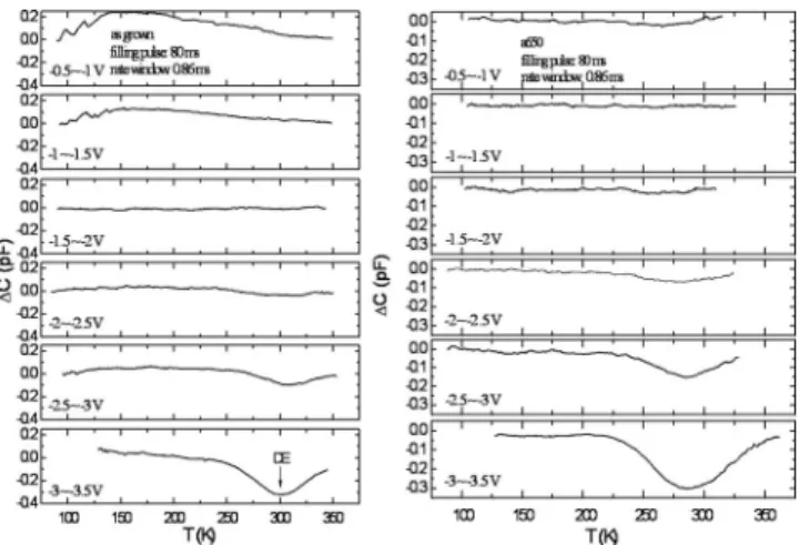
B. DLTS characterization of the misfit defect state Figure2shows the DLTS spectra for the as-grown QDs and a650. To evaluate the spatial location, the quiescent volt-age is decreased with a sweeping step of 0.5 V. The filling pulse duration time is selected to be 80 ms to saturate the intensity of the defect state. Both samples show no signals until the quiescent voltage is decreased to about ⫺3.5 V, corresponding to the starting voltage 共⫺3.5 V兲 of the DE plateau in Fig. 1, and thus the observed trap共at ⬃300 K兲 shall correspond to the DE peak. The Arrhenius plots yield FIG. 1. C-V profiling and converted apparent carrier distributions at 110 K
for relaxed QDs with InAs deposition thickness of 3.3 ML for the as-grown samples and samples annealed at 650 and 700 ° C, respectively. Two capaci-tance plateaus with corresponding carrier peaks, denoted as QE and DE, can be seen. Strain relaxation induces a defect state which causes the DE emis-sion and drastic carrier depletion on the bottom GaAs side.
FIG. 2. DLTS spectra of the relaxed QDs as grown and annealed at 650 ° C, measured at different quiescent voltages with a fixed sweeping step of 0.5 V. In both samples, no signals are observed in the top GaAs layer. For quies-cent voltage of⫺3 V 共⫺3 to ⫺3.5 V兲, a trap signal can be seen at around ⬃300 K with activation energies of 0.38 and 0.36 eV for the as-grown QDs and QDs annealed at 650 ° C, respectively. By comparison with the C-V profiling in Fig.1, this trap corresponds to the DE peak.
063705-2 Chen et al. J. Appl. Phys. 105, 063705共2009兲
filling pulse duration time and found that the amplitude of the defect state saturated when filling pulse duration time was increased to about 1 ms. The feature of saturation sug-gests an isolated point defectlike nature for the misfit defect state. The saturated peak intensity of⌬C=0.3 pF in Fig. 2
yields a sheet density of about 4.1⫻109 cm−2 from NT = ND共⌬C/C02兲A, where ND= 1⫻1017 cm−3, C
0= 200 pF,
area A = 5⫻10−3 cm2, and permittivity =1.14 ⫻10−10 F/m. This density is approximately one order of
magnitude less than the QD sheet density 共about 3 ⫻1010 cm−2 from AFM兲, and thus the concentration of the
defect state is not large enough to cause a complete depletion of the electrons in the QDs. This can explain the observation of the QE peak, consistent with the PL spectra which clearly show the QD ground and first excited transitions at 300 K共to be shown兲.
C. Electron emission from the QDs
We can roughly estimate the density of the electrons accumulated in the QDs by evaluating the underlying area of the QE peak in Fig. 1. From the lowest ac frequency as indicated, we obtain sheet densities of 2.78⫻1011, 2.69 ⫻1011, and 2.06⫻1011 cm−2 for the as-grown QDs and
a650 and a700, respectively. Annealing seems to slightly re-duce the concentration of the electrons in the QDs. A com-parison with the QD density of ⬃3⫻1010 cm−2 suggests
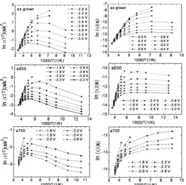
that the electrons fill up to the FES of the QD. The frequency-dependent attenuation of the QE peak allows us to determine the emission time by measuring the conductance as a function of frequency and temperature at the dc voltages corresponding to the QE plateau in Fig.1共⫺2 to ⫺3.4 V for
the as-grown QDs, ⫺1.3 to ⫺3.2 V for a650, and ⫺1.5 to ⫺2.6 V for a700兲. Figure 3 shows the conductance/ frequency-frequency共G/F-F兲 spectra at a dc voltage corre-sponding to the near ending of the QE plateau共the electrons in the QDs are nearly emptied兲 for the as-grown QDS and a650 and a700, respectively. The oscillation level is selected as 10 mV. For each temperature, the G/F curve displays a peak at a frequency corresponding to emission rate. As shown in Fig. 3, for a same temperature, the peak is shifted to a higher frequency after annealing, suggesting that anneal-ing can reduce the emission time. Figure4shows the Arrhen-ius and logarithmic plots of the emission time共the inverse of the emission rate兲 as a function of dc voltage. From the
loga-rithmic plots, the emission time displays a strong ture dependence at a high temperature and a near tempera-ture independence at a low temperatempera-ture. Thus, electron emission from the QDs transits from a thermal emission to a tunneling emission when temperature is lowered. From the Arrhenius plots at high temperatures, the thermal emission energy are obtained to be 91–213 meV from ⫺2 to ⫺3.4 V for the as-grown QDs, 86–193 meV from ⫺1.6 to ⫺3.2 V for a650, and 52–164 meV from ⫺1.6 to ⫺2.6 V for a700. Table I summarizes the bias-dependent emission energies and capture cross sections for the three samples.
The bias-dependent emission energy for the electron emission from the QDs is not due to an electric field effect because increasing the amplitude of the electric field would decrease, not increase, the emission energy. This observation suggests a bandlike electron state for the QDs. As estimated from the area of the QE peak, the QE peak shall consist of the QD EGS and FES. Thus, the observed energy from 91 to 213 meV for the as-grown QDs may represent the two states and the 213 meV is the highest bound of the EGS. As shown in Fig. 1, the QE peak for the as-grown QDs is asymmetric FIG. 3. The G/F-F spectra measured on the QE peaks for the as-grown relaxed InAs QDs and those annealed at 650 and 700 ° C, respectively. The dc voltages correspond to the near emptying of the QD electron GS.
with a right shoulder. When temperature is lowered below 100 K, the QE peak starts to split into two peaks, as shown in Fig.5. Since Fermi level first crosses the higher energy state when reverse dc voltage is applied, the peaks at 0.25 and 0.28 m shall be the QD FES共denoted as ES兲 and the EGS 关denoted as GS 共for ground state兲兴, respectively. Let us try to distinguish the spectral ranges of the two states. In Fig.5共a兲, the indicated voltage of ⫺2.25 V represents the dc voltage for the near emptying of the electrons of the FES and starting to deplete the EGS and the voltage of⫺3.4 V represents the emptying of the EGS. Thus, we use the corresponding emis-sion energy of 119 meV for ⫺2.25 V to separate the two states. As a result, the energy from 91 to 119 meV is consid-ered as the FES and the energy from 119 to 213 meV as the
TABLE I. Electron thermal emission energies and capture cross sections of the QDs, measured at different dc biases for the as-grown samples and samples annealed at 650 and 700 ° C.
3.3 ML, as grown 3.3 ML, annealed at 650 ° C 3.3 ML, annealed at 700 ° C
Bias 共V兲 Ea 共meV兲 Capture cross section 共cm2兲 Bias共V兲 Ea 共meV兲 Capture cross section 共cm2兲 Bias 共V兲 Ea 共meV兲 Capture cross section 共cm2兲 ⫺2 90.64 1.97⫻10−20 ⫺1.3 86.3 2.81⫻10−18 ⫺1.5 51.67 2.91⫻10−19 ⫺2.2 119.35 4.09⫻10−18 ⫺1.4 92.77 3.66⫻10−18 ⫺1.7 70.42 1.56⫻10−18 ⫺2.4 144.03 1.03⫻10−17 ⫺1.6 109.87 1.11⫻10−17 ⫺1.8 87.45 3.15⫻10−18 ⫺2.6 169.47 2.64⫻10−17 ⫺1.8 122.61 1.87⫻10−17 ⫺2.0 91.60 3.51⫻10−18 ⫺2.8 191.56 6.18⫻10−17 ⫺2.2 122.61 1.48⫻10−17 ⫺2.2 95.53 3.72⫻10−18 ⫺3.0 200.27 8.11⫻10−17 ⫺2.4 148.10 4.29⫻10−17 ⫺2.4 112.78 7.02⫻10−18 ⫺3.2 201.88 8.75⫻10−17 ⫺2.6 161.21 7.00⫻10−17 ⫺2.6 164.30 5.36⫻10−17 ⫺3.4 212.74 1.96⫻10−16 ⫺2.8 171.22 1.02⫻10−16 ⫺3.0 184.92 1.84⫻10−16 ⫺3.2 192.71 2.78⫻10−16
FIG. 4. Arrhenius and logarithmic plots of the electron emission times in the relaxed QDs as grown and annealed at 650 and 700 ° C, respectively. The strong temperature dependence at high temperatures suggests a thermal emission. The near temperature independence at low temperatures suggests a tunneling emission.
FIG. 5.共a兲 Temperature-dependent C-V profiling and corresponding 共b兲 car-rier distributions of the as-grown relaxed InAs QDs. When temperature is below 100 K, the QE plateau is split into two plateaus corresponding to the QD FES and the GS. The dc voltage of⫺2.25 V represents the near emp-tying of the FES and the beginning depopulation of the GS. Its correspond-ing emission energy of 119 meV is used to distcorrespond-inguish the two states. The averaged GS and FES are separated by 61 meV.
063705-4 Chen et al. J. Appl. Phys. 105, 063705共2009兲
EGS, yielding spectral broadness of 28 and 94 meV for the FES and EGS, respectively. By taking the averaged value as the energy position, assuming the emission energy is relative to the GaAs CB, the FES and EGS are 105 and 166 meV, respectively, below the GaAs CB, as shown in Fig. 5共a兲. These confinement energies are close to 96 and 190 meV reported by Kapteyn et al.,9and 60 and 140 meV reported by Brunkov et al.26 for similar InAs QDs. This comparability supports the assignment of the QE peak as electron emission from the QDs, rather than from some defect states.
As aforementioned, the misfit defect state is about 0.3 eV below the QE peak state. If we take the FES共105 meV兲 as the peak state, the misfit defect state would be at about 0.4 eV below the GaAs CB, which is close to the activation energy 共0.38 eV兲 of the trap observed by the DLTS. This consistency confirms that the defect state is localized near the QDs and the observed emission is relative to the GaAs CB. In order to confirm whether the electronic band structure in Fig. 5共a兲is related to the FES and EGS of the QDs, we compare it with PL spectra. Figure 6 shows the 300-K PL spectra of the as-grown QDs, a650, and a700, respectively, under the excitation of 3.3 mW. Except for the spectrum for the as-grown QDs, which displays an additional peak at 1307 nm, each spectrum displays the ground 共as indicated by 1215, 1198, and 1170 nm, respectively兲 and first excited tran-sitions of the QDs. The peak at 1307 nm for the as-grown QDs is considered as a transition from another group of the QDs. In order to show this, Fig.7共a兲illustrates the tempera-ture dependence of the as-grown QDS under an excitation power of 10 mW. When temperature is lowered, the ground 共1215 nm兲 and the first excited 共1150 nm兲 transitions signifi-cantly increase in intensity accompanied by a blueshift of about 50 meV 共from 300 to 50 K兲, which is comparable to that observed in nonrelaxed QDs. In comparison, the inten-sity of the transition at 1307 nm only slightly increases, sug-gesting that the related group of the QDs are much smaller in number and are nearly filled up with carriers at 300 K,
rela-tive to the group of the QDs that give the 1215-nm transition. Increasing excitation power can lead to the emergence of the second excited transition of the QD group that gives the 1215-nm ground transition, as shown in the 300-K PL spec-tra in Fig. 7共b兲. The spectra are normalized by the ground transition at 1215 nm to illustrate the relative intensity FIG. 6. 300-K PL spectra of relaxed InAs QDs for the as-grown QDs and
samples annealed at 650 and 700 ° C, respectively. Transitions from the QD GS and FES can be clearly seen. Blueshifts of 15 and 39 meV can be seen after annealing at 650 and 700 ° C, respectively. The inset shows the fitting of the spectra of the annealing at 650 ° C by three Gaussians corresponding to the ground, first excited, and second excited transitions.
FIG. 7. 共a兲 Temperature-dependent PL spectra of the as-grown QDs under an excitation power of 10 mW, illustrating a ground transition at 1215 nm and a first excited transition at 1150 nm.共b兲 Power-dependent PL spectra at 300 K. In order to show the relative intensity change, the spectra are nor-malized by the ground transition关denoted by 共1兲兴. As excitation power in-creases, the first excited关denoted by 共2兲兴 and second excited 关denoted by 共3兲兴 transitions are enhanced with respect to the ground transition. 共c兲 The deconvolution of the 300-K PL spectra.
change. As power increases, in contrast to the transition at 1307 nm, the first excited关indicated by 共2兲兴 and second ex-cited关indicated by 共3兲兴 transitions are enhanced with respect to the ground transition. This feature reflects limited filling of the GS and the filling of the ES by additional photogenerated carriers. Thus, transitions 共1兲–共3兲 should belong to the same group of the QDs. Increasing power does not appreciably enhance the 1307-nm transition, reflecting the fact that the related QDs are very low in number and are already filled up with carriers at low powers. From the deconvoluted 300-K spectra 关Fig. 7共c兲兴, the energy separations between the ground and first excited transitions and between the first and second excited transitions for the predominant group of the QDs are obtained as 59 and 45 meV, respectively, which are close to those observed in nonrelaxed QDs. Thus, the 1215-nm transition is considered as the ground transition of the predominant group of the QDs.
The detailed nature of the transition at 1307 nm is not fully understood. However, it is suspected to be a transition from some QDs that remain nonrelaxed. Note that its wave-length is close to the achievable longest wavewave-length before the onset of strain relaxation. When the InAs deposition thickness is below a critical relaxation thickness of 3 ML, increasing the InAs deposition thickness can redshift the ground transition to about a maximum of 1310 nm共at 300 K兲. When the InAs deposition thickness exceeds 3 ML, the ground transition undergoes a sudden blueshift of about 70 meV due to strain relaxation. Further increasing the InAs deposition thickness can further increase the blueshift. The longest wavelength achievable before strain relaxation is about 1300 nm. Thus, we suspect that at the onset of strain relaxation, due to size dispersion, a few QDs whose size is still below the critical size 共with equivalent wavelength of 1300 nm兲 are probably not relaxed and give rise to the 1307-nm transition. Further increasing the InAs deposition thickness would enhance the degree of strain relaxation and reduce the numbers of these nonrelaxed QDs, which can ex-plain the experimentally observed decreasing intensity of this transition. Figure 6 shows that the 1307-nm transition be-comes invisible after annealing, suggesting that annealing probably can probably provide thermal energy for these re-maining nonrelaxed QDs to relax and to blueshift its transi-tion. In view of the above discussions, the nonrelaxed QDs are very few in number. Electron emission from these non-relaxed QDs is expected to be very weak and fast, and thus electron emission from them is not considered. In fact, as shown in Fig.5共b兲, the carrier distribution at 90 K exhibits a very weak bump at 0.33 m. This bump is seen after the GS
of the relaxed QDs, consistent with its relative long PL wavelength. Thus, this bump is likely related to the 1307-nm transition.
As shown in Fig.6, the ground transition is blueshifted from 1.0206 to 1.0351 eV and further to 1.0598 eV after annealing at 650 and 700 ° C, respectively. This blueshift is usually explained by the interdiffusion of atoms across the QD interface. The observation of these transitions suggests that the QD sates are not severely degraded by strain relax-ation. Thus the electron emission from the related electron states is expected to be observed. We fit each spectrum by three Gaussians corresponding to the ground, first excited, and second excited transitions, as shown in the inset of Fig.
6 for a650. Table II shows the obtained full widths at half maximum共FWHMs兲 of the ground and first excited PL tran-sitions 共denoted as GS and ES兲 for the as-grown QDs and a650 and a700, respectively. For the as-grown QDs, the FWHMs are 68 and 41 meV for the ground and first excited transitions, which are close to 94 and 28 meV for the broad-ness of the QD EGS and FES shown in Fig. 5共a兲. The PL spectra show energy separation of 59 meV between the ground and first excited transitions, which is closed to that of 61 meV between the EGS and FES in Fig. 5共a兲. This com-parability suggests a very small energy separation between the hole GS and FES, as previously claimed.26As shown in Table II, the total FWHM of the ground and first excited transitions for a650 is 107 meV, which is close to the whole range of 106 meV共from 86 to 193 meV兲 observed from the electron-emission energy from the QDs共C-F spectra兲. Simi-lar closeness is observed for a700. This comparison shows comparable broadness and separation of the electron energy states and the corresponding PL transitions, supporting that the QE peak is originated from the QD EGS and FES.
Annealing can decrease the electron-emission energies of the QDs. For example, the highest-bound emission energy of the EGS decreases from 213 to 193 meV and to 164 meV after annealing at 650 and 700 ° C, respectively. This implies upward energy shifts of 20 and 49 meV, which are close to the 300-K PL blueshifts of 15 meV共from 1.0206 to 1.0351 eV兲 and 39 meV 共from 1.0206 to 1.0598 eV兲 as shown in Fig.6. Thus, the reducing emission energy of the QD states can be correlated to the PL blueshift which is attributed to the interdiffusion of atoms across the QD interface. This re-sult suggests that most of the energy shift induced by anneal-ing is in the CB, consistent with the result of a theoretical calculation.27The consistency of the energy shift further sup-ports the assignment of the QE peak as electron emission from the QDs, rather than from the misfit defect state to the QD state as previously suspected.17Since if it were, the up-TABLE II. Ranges of electron thermal emission energies of the QDs and the FWHMs of the PL GS and first
excited state共ES兲 transitions for the as-grown samples and samples annealed at 650 and 700 °C.
As grown a650 a700
C-F 90.6共ES兲–212.7 共GS兲 86.3共ES兲–192.7 共GS兲 51.7共ES兲–164.3 共GS
共Ea兲 䊐E=122.1 meV 䊐E=106.4 meV 䊐E=112.6 meV
PL 68.2共GS兲 and 41.1 共ES兲 77.3共GS兲 and 30.0 共ES兲 67.2共GS兲 and 30.6 共ES兲
共FWHM兲 䊐E=109.3 meV 䊐E=107.3 meV 䊐E=97.8 meV
063705-6 Chen et al. J. Appl. Phys. 105, 063705共2009兲
ward shift of the QD state by annealing as implied by the PL blueshift would increase the emission energy, rather than de-crease as experimentally observed. Hence, the QE peak is proved to be an electron emission from the QDs.
D. Electron emission mechanism from the relaxed QD The logarithmic plots of the emission times in Fig. 4
suggest a combination of a thermal emission and a tunneling emission as expressed by the equation en= eth+ etun.28 Here
eth=␥T2
nexp共−Ea/kT兲 is the thermal emission rate where
␥= 2.28⫻1020 cm−2s−1K−2for n-type GaAs, Eais the ther-mal emission barrier andnis the capture cross section, and
etun=共qF/4
冑
2mⴱEh兲exp关−共4/3兲共冑
2mⴱEh3/qបF兲兴 is the tun-neling emission rate, where F is the electric field and Eh is the tunneling barrier height. From the Arrhenius plots at high temperatures, values of Eaandn have been determined as listed in TableI. Values of the tunneling barrier height Ehcan be fitted by the emission times at low temperatures in Fig.4. We found that the fitted Ehis very close to Ea. This isillus-trated in Fig.8, in which the experimental data points can be fitted by the above theoretical expression共solid curves兲 using
Eh= Ea. To further illustrate this point, Fig.9 shows the ex-perimental tunneling times 共observed at low temperatures兲 for the as-grown QDs and a650 and a700 follow the theoret-ical tunneling time expressiontun= 1/etunwith Eaas Eh. The fact that the thermal emission barrier is the tunneling barrier indicates that at high temperatures, electrons are thermally emitted from the QD states to the GaAs CB. This electron emission process is quite different from that observed in defect-free nonrelaxed QDs.9,17
E. Comparison with defect-free nonrelaxed QDs For comparison, Fig.10shows 80-K C-V profiling and converted electron distribution for a nonrelaxed InAs QDs 共capping with an InGaAs layer兲 with InAs deposition thick-FIG. 8. Logarithmic plots of the electron emission times in the relaxed QDs
for the as grown, annealing at 650 and 700 ° C, respectively. These emission times can be well fitted by a combination of a thermal emission and a tunneling emission with the thermal emission barrier as the tunneling barrier.
FIG. 9. The experimental tunneling times vs the thermal emission energies for the as-grown QDs and QDs after annealing at 650 and 700 ° C, respec-tively. These data points follow the theoretical tunneling expression with the thermal emission barrier as the tunneling barrier.
FIG. 10. Electron distribution and corresponding C-V profiling共in the inset兲 for nonrelaxed InAs QDs with InAs deposition thickness of 2.4 ML. One carrier peak at 0.25 m with a shoulder at 0.26 m is seen. The ES peak is attributed to the electrons tunneling from the QD ESs to the GaAs CB. The GS shoulder is attributed to a thermal excitation from the QD ground to FES and subsequently tunnels to the GaAs CB.
ness of 2.4 ML. Electron emission from the QDs results in a capacitance plateau 共⫺1.5 to ⫺3 V兲 and its corresponding carrier peak at 0.25 m共denoted as ES兲 with a clear shoul-der bump at 0.26 m共denoted as GS兲. Besides this plateau, no further plateau, such as the DE plateau observed in the relaxed QDs, is seen. Furthermore, the carrier depletion is rather symmetric on both sides of the peak. The ES peak is attributed to electrons in the QD ESs tunneling9–11 to the GaAs CB. The emission time of this peak is too short to be resolved up to 1 MHz at 10 K. The GS shoulder shows frequency-dependent attenuation with an emission time on the order of 10−6 s 共at 70 K兲 and with emission energy of ⬃60 meV,17
as indicated in Fig.11. This emission energy is comparable to the PL energy spacing between the ground and first excited transitions, and thus the shoulder bump is attributed to a thermal excitation from the QD EGS to FES and subsequently tunnels to the GaAs CB, in a two-stage emission process previously described,9 as illustrated by a CB schematic diagram共nonrelaxed兲 in Fig.11. The two-step emission mechanism for nonrelaxed QDs was previously corroborated by capping the InAs QDs with an InAlAs layer to increase the energy spacing between the EGS and FES and a comparable increase in this energy spacing and in the en-ergy spacing between the PL ground and first excited transi-tions was ovserved.29 Detailed discussions on the emission process in nonrelaxed QDs can be found elsewhere.9,14
When the InAs deposition thickness exceeds 3 ML, strain relaxation in the QDs occurs, accompanied with a sud-den PL blueshift of about 70 meV in the ground transition18 and the generation of a misfit defect state near the QD if the QD is capped with an InGaAs layer. Without the InGaAs capping layer, strain relaxation would generate additional threading dislocations in the top GaAs barrier layer.30Hence, the InGaAs capping layer can effectively relieve the strain in the top GaAs layer, leading to the occurrence of strain relax-ation near the QD bottom interface. With the InGaAs cap-ping layer, strain relaxation does not deplete much the carri-ers in the QDs. However, the induced misfit defect state can cause additional carrier depletion on the GaAs bottom side and suppress the tunneling emission from the QDs. As a
result, electrons escaping out of the EGS and FES occur through a thermal emission to the GaAs CB 共at high tem-peratures兲, as illustrated in the schematic diagram 共relaxed兲 in Fig. 11, in which the detailed CB protrusion due to the additional carrier depletion is not shown. Highest-bound thermal emission energy of 213 meV is observed for the QD EGS for the as-grown QDs, with respect to 60 meV in the nonrelaxed QDs. Figure 11shows that strain relaxation sig-nificantly elongates the emission time of the QD EGS. An-nealing at 650 ° C can reduce the highest-bound emission energy of the EGS to 193 meV and further to 164 meV after annealing at 700 ° C. Figure11shows the emission times of the EGS for dc biases corresponding to the peak of the EGS. At low temperatures, inevitable tunneling emission appears. The tunneling times for the FES are on the order of 10−6 s, relative to an irresolvable short time in the nonrelaxed QDs. Since annealing does not much affect the concentration and emission parameters of the misfit defect state as implied by the DLTS, the decrease in the emission time and energy by annealing cannot be explained by the effect of the defect state. Judging from a comparable energy blueshift in the PL transition, the decrease in the emission time is attributed to an upward energy shift of the QD electron states due to in-terdiffusion of atoms across the QD interface. The results of the present studies illustrate a significant effect of a defect state on the electron-emission process in the QDs, offering the possibility of modifying the electron emission time of the QDs by purposely introducing a deep defect state.
IV. CONCLUSIONS
Electron distribution and emission in strain relaxed InAs QDs subjected to thermal annealing are investigated. Strain relaxation can introduce additional capacitance plateau due to the generation of a misfit defect state, leading to additional carrier depletion in the GaAs bottom side. This carrier deple-tion can suppress the tunneling emission from the QDs and change the electron emission process. Without the defect state, electrons escape from the GS through a thermal emis-sion to the FES and then tunneling to the GaAs bottom layer. With the defect state, at high temperatures, electrons escape from the GS and FES via a thermal emission to the GaAs CB, leading to a significant increase in the emission time and energy. Annealing can reduce the emission time and energy due to an upward energy shift of the QD electron states, as evident from the observation of a similar energy shift in the PL transitions of the QDs. These results suggest that a defect state can be purposely introduced to modify the electron-emission time of the QDs.
ACKNOWLEDGMENTS
The authors are grateful to Dr. J. Y. Chi and R. S. Hsiao for sample preparation and would like to thank the National Science Council of Taiwan for financially supporting this research under Contract No. NSC-97-2112-M-009-014-MY3. This work was partially supported by MOE ATU pro-gram.
1F. Heinrichsdorff, M. H. Mao, N. Kirstaedter, A. Krost, and D. Bimberg,
FIG. 11. Logarithmic plots of the electron emission times of the QD EGSs for the nonrelaxed InAs QDs共with emission energy of 60 meV兲, and relaxed InAs QDs as grown and annealed at 650 and 700 ° C, respectively. CB schematic diagrams illustrate the emission processes for the nonrelaxed and relaxed InAs QDs.
063705-8 Chen et al. J. Appl. Phys. 105, 063705共2009兲
and J. I. Chyi,Phys. Rev. B64, 125315共2001兲.
12X. Letartre, D. Stievenard, and M. Lanoo,J. Appl. Phys.69, 7336共1991兲. 13H. Drexler, D. Leonard, W. Hansen, J. P. Kotthaus, and P. M. Petroff,
Phys. Rev. Lett.73, 2252共1994兲.
14S. Sauvage, P. Boucaud, F. H. Julien, J.-M. Gerard, and J.-Y. Marzin,J. Appl. Phys.82, 3396共1997兲.
15J. S. Wang, J. F. Chen, J. L. Huang, P. Y. Wang, and X. J. Guo,Appl. Phys. Lett.77, 3027共2000兲.
16Y. Uchida, H. Kakibayashi, and S. Goto,J. Appl. Phys.74, 6720共1993兲. 17J. F. Chen, R. S. Hsiao, C. K. Wang, J. S. Wang, and J. Y. Chi,J. Appl.
P. N. Brunkov, A. Patane, A. Levin, L. Eaves, P. C. Main, Y. G. Musikhin, B. V. Volovik, A. E. Zhukov, V. M. Ustinov, and S. G. Konnikov,Phys. Rev. B65, 085326共2002兲.
27O. Gunawan, H. S. Djie, and B. S. Ooi,Phys. Rev. B71, 205319共2005兲. 28J. Ibanez, R. Leon, D. T. Vu, S. Chaparro, S. R. Johnson, C. Navarro, and
Y. H. Zhang,Appl. Phys. Lett.79, 2013共2001兲.
29J. F. Chen, R. S. Hsiao, M. F. Hsieh, J. S. Wang, and J. Y. Chi,J. Appl. Phys.99, 014303共2006兲.
30J. F. Chen, R. S. Hsiao, W. D. Huang, Y. H. Wu, L. Chang, J. S. Wang, and
J. Y. Chi,Appl. Phys. Lett.88, 233113共2006兲.