Fabrication of sub-60-nm contact holes
in silicon dioxide layers
Fu-Hsiang Ko
a,*, Hsin-Chiang You
b, Tieh-Chi Chu
c, Tan-Fu Lei
b,
Chun-Chen Hsu
c, Hsuen-Li Chen
aa
National Nano Device Laboratories, 1001-1, Ta-Hsueh Road, Hsinchu 300, Taiwan
b
Institute of Electronics Engineering, National Chiao Tung University, Hsinchu 300, Taiwan
c
Department of Atomic Science, National Tsing Hua University, Hsinchu 300, Taiwan Available online 14 March 2004
Abstract
We have developed a fabrication technique, comprising electron-beam writing, chemical shrinking, and silicon dioxide etching, for the fabrication of sub-60-nm contact holes. The dimensions of the contact holes after the electron-beam writing, chemical shrinkage, and plasma etching steps were 140, 93, and 53 nm, respectively. We carefully evaluated the critical process parameters, such as mixing-bake temperature, mixing-bake time, plasma etch selectivity, and the profile shapes. A higher mixing-bake temperature led to an overhang of the contact hole in the resist; the optimal mixing-bake conditions occur when heating at 110°C for 70 s. A fluorinated mixture of gases (CHF3/CF4¼ 1:1) was used to etch the
nano-scale contact holes in the silicon dioxide layer. The formation of side-wall polymers during the plasma etch phase contributed further to the contact hole shrinkage in addition to resist chemical shrinkage. The ratio of the holeÕs perimeter to its area affects the shrinkage dimensions of the etch process, especially for smaller contact holes. The pattern reduction due to side-wall polymer deposition in etch process has the inverse relationship with the diameter of contact hole. Ó 2004 Elsevier B.V. All rights reserved.
Keywords: Electron-beam writing; Chemical shrink; Contact hole; Side-wall polymer
1. Introduction
The progress of research into integrated circuits (ICs) is focused mainly on two goals: (1) increasing circuit performance (mainly by increasing circuit speed) and (2) increasing the functional complexity of the circuits. Scaling down device sizes is
con-sidered a very effective means of achieving these goals, but discovering technologies for achieving sub-60-nm contact holes is still a challenge [1,2].
The ITRS 2002 Update [2] predicts that, for ASIC fabrication, the critical dimensions (CDs) for con-tact holes after etching will be required to be 65 and 45 nm by 2007 and 2010, respectively. Technologies that use chemical shrinkage for patterning sub-100-nm contact holes in resists have been reported previously [3]. In that report, the authors proposed using a polymeric shrinking agent that cross-links on
*
Corresponding author. Tel.: +886-35726100x7618; fax: +886-35722715.
E-mail address:[email protected](F.-H. Ko).
0167-9317/$ - see front matter Ó 2004 Elsevier B.V. All rights reserved. doi:10.1016/j.mee.2004.02.061
the patternÕs sidewalls at a suitable mixing-bake temperature, but such a shrinkage technique faces the problem of defect formation in the resist pattern at higher mixing-baking temperatures. Therefore, such chemical shrinkage technology has not been used previously for the generation of sub-60-nm features. Solving this problem, and to achieve the goal of preparing sub-60-nm contact holes in a sili-con dioxide layer, requires sili-controlling the shrinkage temperature for the ca. 90-nm contact holes in the resist and improving the etch process that allows further shrinkage to occur.
In this paper, we investigate chemical shrinkage process parameters that are used in conjunction with electron-beam lithography for preparing con-tact holes during ASIC fabrication. We have eval-uated the various bake processes and process stabilities, and we discuss the cross-sectional images of holes formed by the chemical shrinkage process at various mixing temperatures. Upon completing the chemical shrinkage procedure, we also evaluated a series of dry etch recipes for the silicon dioxide layer.
2. Experimental
Table 1 lists the experimental flows and param-eters used for preparing the sub-60-nm contact holes in the silicon dioxide layer. Electron-beam exposure was performed on a Leica Weprint 200 stepper. The silicon dioxide layer was grown by wet oxidation using a mixture of hydrogen (8000 cm3/
min) and oxygen (4999 cm3/min) gases at 978°C in
a low-pressure furnace. The electron-beam energy was 40 keV, the beam size was 20 nm, and the ex-posure dose was 14 lC/cm2. The developer for the
JSR positive electron-beam resist (MES-1EG) was an aqueous 2.38% tetramethylammonium hydrox-ide (TMAH) solution. A positive-tone electron-beam resist was spin-coated on a silicon wafer (150 mm diameter) and baked at 110°C for 120 s. The thickness of the resist film was ca. 650 nm. After exposure and a post-exposure bake (110°C for 120 s), the wafer was developed using the TMAH so-lution. Again, a hard-bake was applied to the wafer (110°C for 120 s). A chemical shrinkage procedure was then applied. The chemical shrinking agent (AZ R-200, Clariant) was coated over the resist
pattern, and the wafer was again soft-baked. The film thickness was ca. 400 nm. A mixing-bake step at 110 °C for 70 s was then undertaken. The chemical shrinking agent reacted with the resist acid that diffused from the resist pattern. A cleaning step, using AZ R-2, which can wash away unre-acted materials, was applied to the process. A hard-bake step was performed at 110 °C for 2 min. Finally, we applied a plasma process using a mix-ture of CHF3and CF4gases to etch the underlying
silicon dioxide layer. Critical dimensions were evaluated using either an in-line scanning electron microscope (SEM, Hitachi S-6280) or a cross-sec-tional SEM (Hitachi S-4000).
3. Results and discussion
3.1. Chemical shrinkage processes for the electron-beam resist
As has been reported previously [3], the mixing-bake temperature and time are the critical factors
Table 1
Process conditions for the fabrication of sub-60-nm contact holes in a silicon dioxide layer
Oxidation processes
Oxidation temperature 978°C, SiO2thickness 150 nm
Gas components H2(8000 cm3/min)/O2
(4999 cm3/min) Lithography processes Spin speed 2500–5000 rpm, 30 s Resist thickness 650 nm Exposure dose 14 lC/cm2 Soft-bake 110°C, 120 s Post-exposure bake 110°C, 120 s Development TMAH, 60 s Hard-bake 110°C, 120 s Chemical shrink processes
Soft-bake 85°C, 70 s Mixing-bake 110°C, 70 s
AZ remover (R-2) 10% IPA and 90% H2O,
two puddles 40/20 s Hard-bake 110°C, 120 s Etch and resist stripping processes
Etch time 60 s
Gas components CF4, 20 sccm/CHF3, 20 sccm
Chemicals H2SO4/H2O2¼ 3:1, 120 °C,
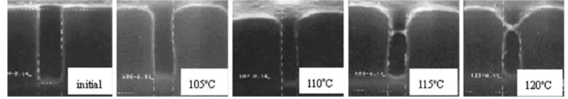
for fabricating sub-100-nm contact holes in a resist when using the chemical shrinkage technique. Basically, the residual acid in the resist pattern diffuses into the side-wall regions of the shrinkage agent, which leads to cross-linkage reactions of the shrinkage agent. The extent of hole shrinkage in the positive resist depends upon the intrinsic acid diffusion behavior, such as its diffusion coefficient, and the time. Fig. 1 illustrates the effect of mixing-bake temperature on the CDs of various contact holes for the positive electron-beam resist. Char-acterization using top-down SEM clearly indicates that the CDs of contact holes at any size gradually narrow as the mixing-bake temperature is in-creased from 100 to 120°C. An initial hole size of 140 nm formed by electron-beam patterning is suitable for shrinking down to the sub-100-nm level. We evaluated the profile of the contact holes at various mixing-bake temperatures by using cross-sectional SEM. The SEM pictures in Fig. 2 clearly illustrate the profile of the contact holes. Initially (prior to applying the chemical shrinkage
agent), the contact holes have vertical sidewalls and a smooth surface. After a 105°C mixing-bake (subsequent to applying the chemical shrinkage agent), the sidewalls and surface covered with shrinkage agent appear to be slightly distorted. When the mixing-bake temperature was increased to 110 °C, the contact holes remain open, but we observe an overhang effect in the contact holes formed after heating at either 115 or 120 °C. We attribute this finding to the effect of thermal flow of the shrinkage agent on the resistÕs sidewalls at higher bake temperatures. This type of defect is not observed when viewing from by SEM from above the surface, but is very apparent from the cross-sectional SEM image. Clearly, the upper limit of the mixing-bake temperature for the chemical shrinkage technique is 110°C.
Fig. 3 demonstrates the effect of mixing-bake times on the CDs of various contact holes for the positive resist at 110°C. We observe that the hole dimensions decrease rapidly during the first 60 s, but then gradually reach a plateau. Therefore, we believe that the optimal time for the mixing-bake process in this study is 70 s. The reason for this trend with respect to mixing-bake time is that the process is dependent on the abundance of diffusion acid in the resist pattern, which is limited. If the amount of acid in the resist is increased, the CD will become narrower. The initial 140-nm hole formed by electron-beam patterning is the only one of the holes that we have studied that is suit-able for being shrunk down to a sub-100-nm hole. Next, we compare the effects of the soft-bake, mixing-bake, and hard-bake processes after ap-plying the chemical shrinkage agent. The control conditions for soft-baking, mixing-baking, and hard-baking are 85°C for 70 s, 110 °C for 70 s, and 110 °C for 2 min, respectively. Fig. 4 clearly indi-cates that the hard-bake temperature has no sig-nificant effect on the hole shrinkage ratio. The
Fig. 2. Cross-sectional SEM image of contact holes in the resist after various mixing-bake temperatures. Fig. 1. Dependence of various mixing-bake temperatures for 70
s on the critical dimensions (CDs) of contact holes formed by the chemical shrinkage technique. The initial hole sizes were 140, 180, 240, and 360 nm, respectively; top-down SEM was used to measure CD.
soft-bake temperature does have a significant effect above 110°C, which we ascribe to the thermal flow effect discussed earlier. Among these baking pro-cesses, the mixing-bake temperature exhibits the most significant effect on the hole shrinkage ratio. The hole shrinkage mechanism is closely de-pendent on the abundance of residual acid in the resist pattern. We exposed the wafer in the clean-room environment (class 10) after initial contact hole definition for various delay hours. Fig. 5 in-dicates that the shrinkage ratio fluctuates between 33% and 34% after various delay times. Although not illustrated here, the SEM images for these holes taken from above are very similar. It has been reported in the literature that a chemically amplified resist is sensitive to the molecular base, and leads to T-top and footing problems for the
positive resist when not immediately developed (post-exposure delay) [4]. The molecular base in the cleanroom might have reacted to some extent with the surface acid. Most acids under the resist film, however, are not influenced by the molecular base from the air in the cleanroom. Therefore, the diffusion of the acids out of the resist still occurs during the mixing-bake process and the delay time has no effect.
3.2. Fabrication of 53-nm contact holes
The fabrication of sub-60-nm contact holes in a silicon dioxide layer by the chemical shrinkage technique has not been reported previously. To ensure the applicability to nano-fabrication tech-niques, the resist should tolerate the etching pro-cess. Fig. 6 depicts the etch selectivity that we estimate from the ratio of the plasma etch rates of silicon dioxide and the positive resist under various mixtures of gases. The selectivity gradually in-creases upon increasing the ratio of CHF3 from 0
to 0.75, and then increases abruptly upon a further increase in the gas ratio to 1. It has been suggested in the literature [5] that oxygen byproducts formed during silicon dioxide etching can react with car-bon residues, especially at fluorine/carcar-bon ratio <2. Hence, the polymer formation blocks any further etching process.
The positive resist (650 nm thick) was coated onto a wafer upon which a silicon dioxide film had been grown. A variably shaped electron-beam was
Fig. 3. Dependence of various mixing-bake times on the CDs of contact holes formed by the chemical shrinkage technique. The initial hole sizes were 140, 180, 240, and 360 nm, respec-tively; top-down SEM was used to measure CD.
Fig. 4. The effects of the various bake processes and tempera-tures on the shrinkage ratios of the contact holes.
Fig. 5. The effect of delay time on the shrinkage ratio (delay time¼ the period of time between the formation of the initial hole in the resist and the application of the shrinkage agent).
used to pattern a 140-nm hole in the positive resist (Fig. 7(a)). The chemical shrinkage process was then undertaken by spin-coating the shrinkage agent onto the resist pattern, followed by a soft-bake at 85°C for 70 s. The wafer was then sub-jected to a mixing-bake at 110 °C for 70 s. The residual acid diffuses out from the resist pattern
into the shrinkage agent, which leads to acid-in-duced cross-linkage reactions taking place. After washing off the unreacted shrinkage agent and baking again at 110°C for 2 min, the contact hole in the resist layer now has a 93-nm diameter (Fig. 7(b)). At the stage, the shrinkage ratio is ca. 33.6%. After the resist pattern had shrunk, the wafer was sent for plasma etching to fabricate a contact hole. Interestingly, the dimension of the contact hole in the silicon dioxide is not 93 nm: Fig. 8 indicates that the hole size is 53 nm. The total shrinkage ratio of the hole diameter after the chemical shrinkage and plasma etch processes is 62.1%. What happens to the contact holes in the silicon dioxide layer during the plasma etch pro-cess? The side-wall deposition of residual polymers during the plasma etch process plays a significant role in narrowing the contact hole dimensions.
The etch mechanism for contact hole fabrica-tion in a silicon dioxide layer is very complicated, with the dimensions of the pattern formed during the etch process being controlled by a balance
Fig. 8. Top-down SEM images of the 53-nm contact hole in the SiO2layer obtained: (a) prior; (b) after stripping of the resist; (c)
cross-sectional SEM image of (b).
Fig. 6. The dry etch selectivity of SiO2 to resist at different
CHF3ratios.
between the amount of polymer deposited and the etch conditions. Explanations have been proposed in the literature [6–9] regarding micro-loading and aspect ratio-dependent etching (ARDE) to explain the observations made during etch processes. Mi-cro-loading describes the variations of the etch rate between areas having different pattern densi-ties, with features in low-pattern-density areas etching faster than features in high-pattern-density areas. Effects that are due to the pattern dimen-sions, which includes effects related to transport of etchant species into the pattern, or transport of etch products out of the pattern, are generally re-ferred to as ARDE. Table 2 lists a series of data
for the contact holes obtained after the chemical shrinkage and dry etch processes. The smaller holes exhibit a higher shrinkage percentage for the etch process than the larger holes. We attribute this observation to the pattern dimension effect. As the pattern size is reduced, the probability for the flux of incoming polymer species to interact with the sidewall of the contact hole increases. Fig. 9 depicts the relationship between the ratio of the hole dimension before and after etching and the ratio of the hole perimeter to the hole area of these nano-scale contact holes. We find that a linear dependence exists for the series of holes studied. This finding suggests the pattern reduction arising from side-wall polymer deposition during the etch process has an inverse relationship to the pattern diameter. The probability of transportation of a polymer species onto the sidewall of a contact hole is related linearly to the inverse of the contact hole size (after chemical shrinking). As a consequence, the contact hole in the silicon dioxide layer be-comes smaller than expected after the etching process. We estimate that the uniformities (1 sig-ma) of the proposed method for contact hole formation after the processes of lithography, chemical shrinkage, and plasma etching are 3.21, 3.16, and 2.76 nm, respectively.
4. Conclusions
We have established a successful fabrication technique for preparing sub-60-nm contact holes in a silicon dioxide layer by electron-beam lithog-raphy. We have discussed in detail the many fac-tors that influence the performance of the
Table 2
The diameters of contact holes formed after the processes of chemical shrinkage and plasma etching in SiO2, and their ratios (R¼ hole
radius)
Hole diameter after chemical shrinkage (x) (nm)
Hole diameter after dry etching in SiO2(y) (nm) y=x(%) Perimeter/area (2pR=pR2) 246 233 94.7 0.0163 149 128 85.9 0.0268 133 98 73.6 0.0301 119 79 66.6 0.0336 93 53 53.3 0.0430
Fig. 9. Linear dependence between the ratio of the hole di-mension after and before etching and the ratio of the hole pe-rimeter to hole area during the etching of the nano-scale contact holes.
shrinkage process, such as the mixing-bake tem-perature, mixing-bake time, and hole dimensions before and after chemical shrinkage. Using this chemical shrinkage technique (mixing-bake of 110 °C for 70 s) and an etch gas of CHF3/CF4(1:1), we
obtained a minimum hole dimension of 53 nm. This technology meets the requirements [2] for contact hole fabrication in the year 2009. We propose that a nano-hole effect occurs during the etch-assisted shrinkage reaction because smaller holes have a higher percentage of polymer depo-sition in the resist sidewall than do larger holes.
Acknowledgements
The authors thank the National Science Coun-cil, Taiwan, for supporting this research financially through Contract No. NSC92-2722-2317-200.
References
[1] T. Ishibashi, T. Toyoshima, N. Yasuda, T. Kanda, H. Tanaka, Y. Kinoshita, N. Watase, R. Eakin, Jpn. J. Appl. Phys. 40 (2001) 419.
[2] Semiconductor Industry Association, International Tech-nology Roadmap for Semiconductor 2002 Updated, SIA publication, 2002, p. 56.
[3] H.-L. Chen, F.-H. Ko, L.-S. Li, C.-K. Hsu, B.-C. Chen, T.-C. Chu, Jpn. J. Appl. Phys. 41 (2002) 4163.
[4] P. Rai-Choudhury, Handbook of Microlithography, Mi-cromachining and Microfabrication, Vol. 1: Microlithogra-phy, SPIE Press, WA, 1997 (Chapter 4).
[5] H. Xiao, Introduction to Semiconductor Manufacturing Technology, Prentice Hall, NJ, 2001 (Chapter 9).
[6] R.J. Davis, Appl. Phys. Lett. 59 (1991) 1717.
[7] R.A. Gottscho, C.W. Jurgensen, D.J. Vitkavage, J. Vac. Sci. Technol. B 10 (1992) 2133.
[8] K. Kurihara, M. Sekine, Plasma Sources Sci. Technol. 5 (1996) 121.
[9] S. Samukawa, T. Mukai, J. Vac. Sci. Technol. B 18 (2000) 166.