Research Article
Enabling Lambertian-Like Warm White Organic Light-Emitting
Diodes with a Yellow Phosphor Embedded Flexible Film
Cheng-Chang Chen,
1Huang-Yu Lin,
2Cheng-Hung Li,
1Jin-Han Wu,
1Zong-Yi Tu,
2Li-Ling Lee,
1Ming-Shan Jeng,
1Chien-Chung Lin,
3Jwo-Huei Jou,
4and Hao-Chung Kuo
21Green Energy and Environment Research Laboratories, Industrial Technology Research Institute (ITRI), 195, Section 4, Chung Hsing Road, Chutung 31040, Taiwan
2Department of Photonics and Institute of Electro-Optical Engineering, National Chiao Tung University, Hsinchu 30010, Taiwan 3Institute of Photonic System, National Chiao Tung University, Tainan 711, Taiwan
4Department of Materials Science and Engineering, National Tsing Hua University, Hsinchu 30013, Taiwan
Correspondence should be addressed to Chien-Chung Lin; [email protected]
Received 14 March 2014; Revised 26 May 2014; Accepted 17 June 2014; Published 16 July 2014
Academic Editor: Liang-Sheng Liao
Copyright © 2014 Cheng-Chang Chen et al. This is an open access article distributed under the Creative Commons Attribution License, which permits unrestricted use, distribution, and reproduction in any medium, provided the original work is properly cited.
We demonstrate in this report a new constructive method of fabricating white organic light-emitting devices (OLEDs) with a flexible plastic film embedded with yellow phosphor. The flexible film is composed of polydimethylsiloxane (PDMS) and fabricated by using spin coating followed by peeling technology. From the results, the resultant electroluminescent spectrum shows the white OLED to have chromatic coordinates of 0.38 and 0.54 and correlated color temperature of 4200 K. The warm white OLED exhibits the yield of 10.3 cd/A and the luminous power efficiency of 5.4 lm/W at a luminance of 1000 cd/m2. A desirable Lambertian-like far-field pattern is detected from the white OLEDs with the yellow phosphor containing PDMS film. This method is simple, reproducible, and cost-effective, proving to be a highly feasible approach to realize white OLED.
1. Introduction
In recently years, there have been great demands to replace the traditional lighting sources with more energy efficient ones. White organic light-emitting devices (OLEDs) are one of the most promising technologies for display and lighting applications owing to their advantages of low power consumption, large viewing angle, high contrast ratio, and short response time. Thus, the OLED has been considered as a possible solution for the next generation of light sources [1–
3]. To meet the required standard, the electroluminescence (EL) of OLEDs should contain broad emissions that cover the entire visible range of the spectrum with Commission International de l’Eclairage (CIE) chromaticity coordinates of (0.33, 0.33).
Many methods have been developed to generate the white light emission of OLED by the partial energy trans-fer, such as host materials that are doped with fluores-cence/phosphorescence dyes [4–13]. Several researchers have
developed the mixing of the EL from the host molecules with the excimer/exciplex emissions to yield white light emission [14–16]. Other methods are to stack red-, green-, and blue-emissive components to fabricate OLEDs. By stacking RGB components and charge generation layer (CGL), a tandem structure could demonstrate good luminous efficiency [17–
22]. However, the tandem structure has a major challenge of carrier transport in the junction interface and the multiple-stacking structure is complex.
On the other hand, the white light LEDs combined blue GaN chip and phosphors are quite common [23] and commercially available these days. This technology is mature and applied widely in many fields. In this study, a novel method to combine the feature of OLED and phosphor-based technology is proposed and demonstrated.
The fabrication of the phosphor embedded PDMS film of white OLED is easy to correlate the ordinary process of white OLED. A simplest white OLED consists of two kinds of emissive layer which can emit the complementary color light:
Volume 2014, Article ID 851371, 6 pages http://dx.doi.org/10.1155/2014/851371
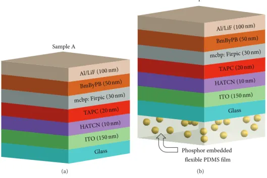
Sample A Al/LiF (100nm) BmByPB (50nm) mcbp: Firpic (30 nm) TAPC (20nm) HATCN (10nm) ITO (150 nm) Glass (a) Phosphor embedded flexible PDMS film Al/LiF (100 nm) BmByPB (50 nm) mcbp: Firpic (30nm) TAPC (20 nm) HATCN (10 nm) ITO (150 nm) Glass (b)
Figure 1: Schematic structures of OLEDs device (a) without a yellow phosphor embedded flexible film as a reference and (b) with a yellow phosphor embedded flexible film.
blue and yellow. Each layer of organic materials was subject to temperature-gradient sublimation under high vacuum before use. The organic layer and metal layers were deposited by vacuum vapor deposition in a vacuum chamber. Fabricating white OLED is complicated due to the modification of multi-emissive layers. The PDMS film is also easy to fabricate and has the ability to resist moisture and heat resistance. The large-area and cost-effective phosphor-embedded PDMS film is utilized to attach with regular OLED cell to provide a new direction for light sources. In the following test, the fabrication steps and results will be discussed in detail.
2. Materials and Fabrication Process
The blue fluorescence of the bottom-emitting OLEDs without PDMS film was fabricated as a reference. Each layer of organic materials was subject to temperature-gradient sublimation under high vacuum before use. OLEDs were fabricated on the ITO-coated glass substrates between the transparent bottom indium-tin-oxide (ITO) anode and the top metal cathode. The organic and metal layers were deposited by vacuum vapor deposition in a vacuum chamber with a base pressure of <106torr. The deposition system permitted the fabrication of the complete device structure in a single vacuum pump-down without breaking vacuum. The deposition rate of organic layers was kept at∼0.1 nm/s. The active area of the device is 0.3 × 0.3 cm2, which is defined by the shadow mask for cathode deposition. After fabricating the OLED devices, the method of glass-to-glass OLED package with desiccant was used in a glove box. Before packing, the glass would be pretreated by solvent cleaning and UV-curing in order to
remove the moisture and particle, increasing the adhesion between the glass lid and substrate, simultaneously. Then we used the packing machine to drop the UV glue on the substrate and made the glass lid and substrate closer by exerting forward force. Finally, the device was treated with UV curing of 110 seconds.
The OLED device structures were glass substrate/ITO (150 nm)/HATCN (10 nm)/TAPC (30 nm)/mcbp: FIrpic (10 wt.%, 20 nm)/BmByPB (50 nm)/LiF (1 nm)/Al (100 nm)/. Indium-tin-oxide (ITO) was used as the bottom anode, Dipyrazino[2,3-f:2,3 -h]quinoxaline-2,3,6,7,10,11-hexacarb-onitrile(HATCN) as the hole-injection layer, 4,4 -cyclohex-ylidenebis[N,N-bis(4-methylphenyl)benzenamine](TAPC) as the hole-transport layer, 3,5-di(9H-carbazol-9-yl)biph-enyl(mcbp): bis(3,5-difluoro-2-(2-pyridyl)phenyl-(2-carbox-ypyridyl)iridium(III)(FIrpic) as the emitting layer, 1,3-bis[3,5-di (pyridin-3-yl)phenyl]benzene(BmByPB) as the electron-transport layer, thin LiF as the electron injection layer, and Al as the top cathode. Illustrations of the reference and white light OLEDs structures are shown in Figures1(a)
and1(b), respectively.
The flexible PDMS film was fabricated using the spin coating and peeling technology as the following steps [23]. First, yellow phosphor (Y3Al5O12:Ce3+) with the particle size of 10𝜇m is blended with the silicone to form the phosphor-suspension slurry. Then the solution is dropped and spin coated for 500 rpm for 30 s on the glass substrate, and then baked it in an oven at about 80∘C. Finally, the PDMS film is peeled off from the glass substrate then put the film on the OLED’s glass substrate.Figure 2shows the magnified image of the PDMS film from an angle-view. The size distribution of yellow phosphor embedded in PDMS film can also been
100 𝜇m
220 𝜇m
Figure 2: The angle-view SEM image of the yellow phosphor embedded flexible PDMS film.
400 450 500 550 600 650 700 750 0.0 0.2 0.4 0.6 0.8 1.0 1.2 N o rm alized EL in te n si ty (a.u .) Wavelength (nm) Sample A Sample B (a) Sample A Sample B 0 10 20 30 40 50 0 1000 2000 3000 4000 5000 6000 7000 L umina n ce (cd/m 2 )
Current density (mA/cm2)
(b) Sample A Sample B 0 10 20 30 40 50 0 2 4 6 8 10 12 L umino us efficienc y (cd/A)
Current density (mA/cm2)
(c) Sample A Sample B 0 10 20 30 40 50 0 2 4 6 8 10 12 L umino us p o w er efficienc y (lm/W)
Current density (mA/cm2)
(d)
Figure 3: (a) The measured EL spectra in the normal direction of Sample A and Sample B. (b) Luminance, (c) current efficiency, and (d) luminous power efficiency characteristics of Sample A and Sample B as a function of current density.
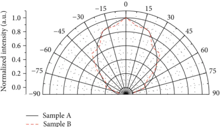
0.0 0.2 0.4 0.6 0.8 1.0 −90 −75 −60 −45 −30 − 15 0 15 30 45 60 75 90 N o rm alized in te n si ty (a.u .) Sample A Sample B
Figure 4: Measured far-field pattern for the OLEDs devices of Sample A and Sample B.
0.0 0.1 0.2 0.3 0.4 0.5 0.6 0.7 0.8 0.0 0.2 0.4 0.6 0.8 1.0 (0.38, 0.54) (0.19, 0.39) y x CIE Illuminant Sample A Sample B (0.33, 0.33) (a) (b) (c)
Figure 5: (a) The CIE coordinates of Sample A and Sample B. (b) The blue light photography of Sample A. (c) Warm white light photography of Sample B.
seen inFigure 2, in which yellow phosphor has a size of 10𝜇m. The thickness of the PDMS layer is measured approximately 220𝜇m.
3. Results and Discussion
To characterize the light emission properties of white organic light-emitting devices, a UV/VIS spectrometer was used and two OLEDs devices (samples A and B) were prepared. Sample B is the organic light-emitting diode with a yellow phos-phor embedded PDMS film and Sample A has an identical OLEDs device without flexible PDMS film.Figure 3(a)shows the electroluminescent (EL) measured spectra from OLEDs devices of Sample A (black curve) and Sample B (red curve) in the normal direction. The wide spectral of the Sample B becomes broad and the emitting wavelength has a red shift that can be seen as energy transfer between the blue OLED and phosphor.
As expected, the emission peaks of Sample A are 470 nm and 500 nm. The emission peak of Sample B is 525 nm, and the spectrum has the visible range from 400 nm to 750 nm due to color mixing.
The luminance current efficiency and luminous power efficiency as a function of current density of the OLEDs device were investigated. Figures 3(b), 3(c), and 3(d)show the results of Sample A and Sample B measured in the nor-mal direction. As presented, Sample A has high luminance and maximum luminous efficiency over 5,000 cd/m2 and 16.5 cd/A. Sample B has a yield of 10.3 cd/A at a luminance of 1000 cd/m2. The maximum luminous power efficiencies of Sample A and Sample B are 9.4 lm/W with the current density of 7.9 mA/cm2 and 5.4 lm/W with the current density of 9.9 mA/cm2, respectively. The phosphoresce emission OLED containing FIrpic has the lifetime of 200 hr [24]. The lifetime of both Sample A and Sample B is the same.
The measured far-field emission profiles of Sample A and Sample B are shown inFigure 4. As shown inFigure 4, Sample A has the Lambertian-like radiation pattern at the full-width at half-maximum of±30∘ along the surface normal view. A desirable Lambertian-like far-field pattern is also observed from Sample B due to the randomness particles of phosphor embedded flexible PDMS film. The CIE coordinates of EL at normal direction from Sample A and Sample B are at (0.19, 0.39) and (0.38, 0.54) with correlated color temperature of 4200 K, shown inFigure 5(a). The CIE coordinates of EL from sample A was obviously shifted and, hence, the corresponding emission color is changed.
Figures5(b)and 5(c)show the photography of OLEDs devices during measurement. Blue light and warm white light regions are corresponding to Sample A and Sample B. The combination of OLEDs with a yellow phosphor embedded flexible film possesses many possibilities for in solid state lighting.
4. Conclusions
In summary, a warm white organic light-emitting diode was demonstrated by attaching a yellow phosphor embedded flexible PDMS film. The flexible PDMS film was fabricated
using the spin coating and peeling technology. From the mea-sured results, the warm white organic light-emitting diode has an efficiency of 10.3 cd/A, luminous power efficiency of 5.4 lm/W, and the CIE coordinate of (0.38, 0.54) with correlated color temperature of 4200 K at a luminance of 1000 cd/m2. We believe that this approach of the fabricating method offers a viable solution to realize that white OLEDs and Lambertian-like profile shaping are suitable for applica-tions in lighting and displays.
Conflict of Interests
The authors declare that there is no conflict of interests regarding the publication of this paper.
Acknowledgment
The authors would like to gratefully acknowledge the Bureau of Energy, Ministry of Economic Affairs of Taiwan, for financially supporting this research.
References
[1] J. Kido, M. Kimura, and K. Nagai, “Multilayer white light-emitting organic electroluminescent device,” Science, vol. 267, no. 5202, pp. 1332–1334, 1995.
[2] B. W. D’Andrade and S. R. Forrest, “White organic light-emitting devices for solid-state lighting,” Advanced Materials, vol. 16, no. 18, pp. 1585–1595, 2004.
[3] C. W. Ko and Y. T. Tao, “Bright white organic light-emitting diode,” Applied Physics Letters, vol. 79, p. 4234, 2001.
[4] J. Kido, K. Hongawa, K. Okuyama, and K. Nagai, “White light-emitting organic electroluminescent devices using the poly(N-vinylcarbazole) emitter layer doped with three fluorescent dyes,”
Applied Physics Letters, vol. 64, no. 7, pp. 815–817, 1994.
[5] J. Kido, H. Shionoya, and K. Nagai, “Single-layer white light-emitting organic electroluminescent devices based on dye-dispersed poly(N-vinylcarbazole),” Applied Physics Letters, vol. 67, no. 16, p. 2281, 1995.
[6] S. Tokito, T. Iijima, T. Tsuzuki, and F. Sato, “High-efficiency white phosphorescent organic light-emitting devices with greenish-blue and red-emitting layers,” Applied Physics Letters, vol. 83, no. 12, pp. 2459–2461, 2003.
[7] L. Wang, G. Lei, and Y. Qiu, “Bright white organic light-emitting diodes based on two blue emitters with similar molecular structures,” Journal of Applied Physics, vol. 97, no. 11, Article ID 114503, 2005.
[8] Y. Sun, N. C. Giebink, H. Kanno, B. Ma, M. E. Thompson, and S. R. Forrest, “Management of singlet and triplet excitons for efficient white organic light-emitting devices,” Nature, vol. 440, no. 7086, pp. 908–912, 2006.
[9] J. Huang, W. J. Hou, J. H. Li, G. Li, and Y. Yang, “Improving the power efficiency of white light-emitting diode by doping electron transport material,” Applied Physics Letters, vol. 89, no. 13, Article ID 133509, 2006.
[10] J. H. Seo, J. H. Park, Y. K. Kim et al., “Highly efficient white organic light-emitting diodes using two emitting materials for three primary colors (red, green, and blue),” Applied Physics
role possessed di(triphenyl-amine)-1,4-divinyl-naphthalene,”
Organic Electronics, vol. 8, no. 6, pp. 735–742, 2007.
[12] J. H. Jou, Y. S. Chiu, C. P. Wang, R. Y. Wang, and H. C. Hu, “Efficient, color-stable fluorescent white organic light-emitting diodes with single emission layer by vapor deposition from solvent premixed deposition source,” Applied Physics Letters, vol. 8, Article ID 193501, 2006.
[13] Y. C. Tsai and J. H. Jou, “Long-lifetime, high-efficiency white organic light-emitting diodes with mixed host composing double emission layers,” Applied Physics Letters, vol. 89, Article ID 243521, 2006.
[14] B. W. D’Andrade, J. Brooks, V. Adamovich, M. E. Thompson, and S. R. Forrest, “White light emission using triplet excimers in electrophosphorescent organic light-emitting devices,”
Advanced Materials, vol. 14, no. 15, pp. 1032–1036, 2002.
[15] E. L. Williams, K. Haavisto, J. Li, and G. E. Jabbour, “Excimer-based white phosphorescent organic light emitting diodes with nearly 100 % internal quantum efficiency,” Advanced Materials, vol. 19, no. 2, pp. 197–202, 2007.
[16] J. Kalinowski, M. Cocchi, D. Virgili, V. Fattori, and J. A. G. Williams, “Mixing of excimer and exciplex emission: a new way to improve white light emitting organic electrophosphorescent diodes,” Advanced Materials, vol. 19, no. 22, pp. 4000–4005, 2007.
[17] Z. Shen, P. E. Burrows, V. Bulovi´c, S. R. Forrest, and M. E. Thompson, “Three-color, tunable, organic light-emitting devices,” Science, vol. 276, no. 5321, pp. 2009–2011, 1997. [18] L. S. Liao, K. P. Klubek, and C. W. Tang, “High-efficiency
tandem organic light-emitting diodes,” Applied Physics Letters, vol. 84, no. 2, pp. 167–169, 2004.
[19] H. Kanno, R. J. Holmes, Y. Sun, S. Kena-Cohen, and S. R. Forrest, “White stacked electrophosphorescent organic light-emitting devices employing MoO3 as a charge-generation layer,”
Advanced Materials, vol. 18, no. 3, pp. 339–342, 2006.
[20] M. H. Ho, T. M. Chen, P. C. Yeh, S. W. Hwang, and C. H. Chen, “Highly efficient p-i-n white organic light emitting devices with tandem structure,” Applied Physics Letters, vol. 91, no. 23, Article ID 233507, 2007.
[21] T. W. Lee, T. Hoh, B. K. Choi, M. S. Kim, D. W. Shin, and J. Kido, “High-efficiency stacked white organic light-emitting diodes,”
Applied Physics Letters, vol. 92, no. 4, Article ID 043301, 2008.
[22] L. Liao, W. K. Slusarek, T. K. Hatwar, M. L. Ricks, and D. L. Comfort, “Tandem organic light-emitting diode using hexaaza-triphenylene hexacarbonitrile in the intermediate connector,”
Advanced Materials, vol. 20, no. 2, pp. 324–329, 2008.
[23] K. Chen, H. Chen, K. Tsai et al., “Resonanta-enhanced fulla-color emission of quantuma dot-based display technology using a pulsed spray method,” Advanced Functional Materials, vol. 22, no. 24, pp. 5138–5143, 2012.
[24] M. S. Weaver, Y. J. Tung, B. D’Andrade et al., “11.1: invited paper: advances in blue phosphorescent organic light−emitting devices,” SID Symposium Digest of Technical Papers, vol. 37, no. 1, pp. 127–130, 2006.