1154 IEEE ELECTRON DEVICE LETTERS, VOL. 34, NO. 9, SEPTEMBER 2013
Electrical Performance Enhancement of
Al–Zn–Sn–O Thin Film Transistor by
Supercritical Fluid Treatment
Li-Feng Teng, Po-Tsun Liu, Senior Member, IEEE, and Wei-Ya Wang
Abstract— In this letter, a low-temperature supercritical fluid
(SCF) treatment was employed to enhance the electrical and opti-cal properties of amorphous Al–Zn–Sn–O thin film transistors (a-AZTO TFTs) for flat-panel displays. The carrier mobility and threshold voltage of a-AZTO TFT were improved significantly after SCF process because of the reduction of trap density in the a-AZTO active layer. In addition, the SCF-treated a-AZTO TFT exhibited superior electrical reliability and less degradation after negative gate bias illumination stress. X-ray photoelectron spectroscopy analysis confirmed that the proposed SCF treatment could effectively oxidize a-AZTO film and change the oxidation states of Sn, resulting in the improvement of a-AZTO TFT device characteristics.
Index Terms— Al–Zn–Sn–O thin film transistor (Al–Zn–Sn–O
TFT), supercritical fluid (SCF), transparent amorphous oxide semiconductor (TAOS).
I. INTRODUCTION
T
HIN film transistors (TFTs) using transparent amorphous oxide semiconductor (TAOS) have attracted great atten-tions for the backplane technology of a large-sized liquid-crystal displays and active matrix organic light-emitting diode displays because of its superior characteristics of high mobil-ity, room temperature deposited, good uniformmobil-ity, and com-patibility with present display industry [1]–[3]. Transparent metal oxide TFTs using In–Zn–O [4], Hf–In–Zn–O [5], In–Zn–Sn–O [6], and In–Ga–Zn–O [7] as an active channel layer have been widely studied in the recent years. Although those TFTs performed good electrical performance, containing the rare-dispersive elements will be a critical issue for the long-term applications [8]. Therefore, rare elements-free transparent metal oxide semiconductors are considered to be the promising candidates for the next generation display technologies [9]. In this letter, a TAOS material, Al–Zn–Sn–O (AZTO), is employed as active channel layer of TFTs. All components in AZTO are plenty and universal in the earth. Some previous literatures reported AZTO active layer could be deposited at room temperature and the TFTs exhibit prominent electricalManuscript received June 18, 2013; revised June 30, 2013; accepted June 30, 2013. Date of publication August 2, 2013; date of current version August 21, 2013. This work was supported by the National Science Council of Taiwan under Contract NSC 100-2628-E-009-016-MY3. The review of this letter was arranged by Editor K.-S. Chang-Liao.
L.-F. Teng is with the Department of Photonics and Institute of Electro-Optical Engineering, National Chiao Tung University, Hsin-Chu 30010, Taiwan.
P.-T. Liu and W.-Y. Wang are with the Department of Photonics and Display Institute, National Chiao Tung University, Hsin-Chu 30010, Taiwan (e-mail: [email protected]).
Digital Object Identifier 10.1109/LED.2013.2272117
performance [10]. In this letter, a supercritical fluid (SCF) technology is proposed at 150 ◦C to enhance the electrical performance and reliability of AZTO TFTs. The SCF provides good liquid-like solvency and high gas-like diffusivity, giving it excellent transport capacity [11], [12]. The oxidant is also easily dissolved in SCF with specific surfactants. It is thereby allowed for the SCF to transport the oxidant and penetrates the active layer for trap passivation and interface oxidation at low temperature for promoting the electrical characteristics of AZTO TFT. Photoreaction of the SCF-treated AZTO TFT also is discussed to further examine the potential of AZTO TFT for flat-panel display backplane technologies.
II. DEVICEFABRICATION
TFT devices were fabricated on the silicon wafer with a bottom-gated inverted-staggered structure. First, a 100-nm-thick thermal oxide was thermally grown on n+ heavily doped (100) silicon substrate, which acted as a gate electrode. The active channel layer of a 25-nm-thick AZTO layer was formed by RF reactive sputtering with a power of 80 W at room temperature in a mixture of argon and oxygen with target of 3:67:30 mol% (Al2O3:ZnO:SnO2). The flow rates of
argon and oxygen gases were 10 and 2 SCCM, respectively. Then, a 100-nm-thick indium tin oxide was formed serving as source/drain electrodes by RF sputtering system and all the layers were defined by shadow masks. Both the channel width and length of AZTO TFTs were varied from 1000 to
200 μm. Sequentially, all samples were thermally annealed
at 450 °C for 1 h in a furnace with N2 gas flow rate of
10L/h under atmosphere pressure, and denoted as the standard samples. It was followed that the samples were posttreated and divided into two groups for study in this letter. In the first group, the sample was placed in a SCF system at 150 °C for 1 h, where it was injected with 2000–3000 psi of super-critical CO2 (SCCO2) fluid that were mixed with 5 vol% of
propyl alcohol and 5 vol% of pure H2O. The propyl alcohol
acts as a surfactant between nonpolar-SCCO2fluid and
polar-H2O molecules, such that the H2O molecules are uniformly
distributed in supercritical CO2 fluid. The SCCO2fluid acted
as a transporter to carry the H2O molecules into metal oxide
films [13]. In the second group, samples were immersed in pure H2O vapor at 150 °C for 1 h for comparison to clarify
the effects of H2O vapor. All electrical measurements were
carried out by using the semiconductor parameter analyzer, Keithley 4200. The material analysis of X-ray photoelectron
TENG et al.: ELECTRICAL PERFORMANCE ENHANCEMENT OF Al–Zn–Sn TFT 1155 Gate Voltage (V) -10 0 10 20 30 40 Drain Current (A) 10-13 10-12 10-11 10-10 10-9 10-8 10-7 10-6 10-5 10-4 10-3 Standard SCF Water vapor Stress Time (s) 0 500 1000 1500 2000
Threshold Voltage Shift
(V) -1 0 1 2 3 4 5 PGBS_Standard PGBS_SCF PGBS_Water vapor NGBS_Standard NGBS_SCF NGBS_Water vapor (b) (a)
Fig. 1. (a) Drain current (ID) versus gate voltage (VG) curves of a-AZTO
TFT devices with different posttreatments at a drain-to-source voltage of 11 V. Inset: device parameters, including threshold voltage (Vth), subthreshold swing (SS), and mobility (μ). (b) Threshold voltage shifts of a-AZTO TFT devices with different posttreatments as a function of gate bias stress. The conditions of GBS test were under the positive and negative gate bias with an electrical field of 2.5 MV/cm and source/drain were grounded for 2000 s.
Fig. 2. XPS analysis of Sn 3d5/2spectrum for the a-AZTO thin films after (a) standard process, (b) SCF posttreatment, and (c) water vapor treatment.
spectroscopy (XPS) was also performed to examine the evo-lution of chemical bondings for 25 nm-thick AZTO thin films with different posttreatments.
III. RESULTS ANDDISCUSSION
Fig. 1(a) shows the transfer characteristics of AZTO TFTs with different posttreatments. The drain-to-source voltage
(VDS) was 11 V. The extracted threshold voltage (Vth),
sub-threshold swing (SS), and carrier mobility of each AZTO TFT are also compared in the inset. The mobility was extracted by the slope of |ID|1/2 − VG plot as equation,
μ = 2L/WCOX(∂|ID|1/2/∂VG)2. It is clearly observed that
after SCF process, the threshold voltage of AZTO TFT decreased from 10.84 to 4.93 V, and the value of SS also was improved from 1.76 to 0.77 V/decade. In addition, the mobility was enhanced significantly from 3.16 to 5.51 cm2/Vs. Trap densities (Nt) can be estimated from SS value with the follow-ing formula. SS= loge10 × (kBT /e)[1 + e(tNt+ Dit)/Ci], where kBis the Boltzmann constant, T is the temperature, e is
the elementary electric charge, t is the thickness of the AZTO active layer, and Dit is the interface trap density, assuming
the trap tNt dominated and Dit is negligible [14], [15].
Gate Voltage (V)
-20 -10 0 10 20 30 40
Drain Current (A)
10-13 10-12 10-11 10-10 10-9 10-8 10-7 10-6 10-5 10-4 Dark 800 nm 700nm 600 nm 550 nm 500 nm 450 nm 400 nm Stress Time (s) 0 500 1000 1500 2000
Threshold Voltage Shift (v)-6
-4 -2 0 Standard SCF Water vapor (b) (a) Optical band-gap (eV) Standard 3.61 SCF 3.68 Water vapor 3.62
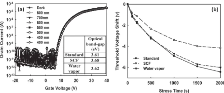
Fig. 3. (a) Transfer characteristics of the a-AZTO TFTs without any posttreatments under light radiation. Inset: corresponding values of opti-cal energy bandgap (Eg) of a-AZTO films after different posttreatments.
(b) Threshold voltage shifts of a-AZTO TFT devices with different posttreat-ments as a function of negative GBS under light illumination.
The Nt value of a-AZTO TFT for the standard, SCF-treated,
and the water vapor process was 1.02 × 10¹⁸, 2.48× 10¹⁸, and 1.49 × 1018 cm−3, respectively. This indicated that the proposed SCF treatment effectively decreased the trap density of AZTO active layer and improved the electrical performance of AZTO TFTs. In contrast, the performance of AZTO TFTs with H2O vapor treatment was also improved. Chen et al.
[11] reported that the H2O absorbed in metal oxide thin films
was dissociated into H and OH groups. The hydrogen atoms could be incorporated into metal oxide thin film to form hydrogen-related donors, whereas the dangling bonds or traps in the metal oxide thin film could be passivated by OH and form M–OH bonds (M is a metal cation). The passivation effect of OH on the amorphous AZTO film with large amount of dangling bonds will be more significant. In addition, Nomura et al. [14] reported that the OH bonds in metal oxide film would react with neighboring hydrogen and generate H2O
molecules by the following equation: M−OH+ M−OH → Vö+ M − O − M + H2O↑ +2e−, where M is a metal cation
and Vö is an ionized oxygen vacancy. It was also consisted
with the experiment results, both SCF and H2O vapor could
improve the electrical performance of AZTO TFTs. The results of gate bias stress (GBS) are shown in Fig. 1(b). In this measurement, an electric field of 2.5 MV/cm was applied to gate electrode and source/drain electrodes were grounded. The instability of SCF treated a-AZTO TFT was improved effectively, and the value of Vthshift after positive GBS testing
was 2.81 V, whereas it was 4.15 V for the a-AZTO TFT without SCF treatment. Comparatively, the improvement in
Vth shift was not observed for the H2O vapor-treated one.
It indicated that the effects of SCF treatment were dif-ferent from the H2O vapor treatment. The XPS analysis
was used further to identify the physical mechanism for electrical enhancement of a-AZTO TFTs. Fig. 2 shows the XPS of Sn 3d5/2 spectrum for the a-AZTO thin film
with different posttreatments. The peak of Sn 3d5/2 signal
has two components with binding energies of 486.6 and 485.9 eV, respectively, which were fitted by Gaussian– Lorentzian deconvolution. The higher binding energy centered at 486.6 is originated from the Sn4+ bonding state, whereas the lower binding energy centered at 485.9 is attributed to the Sn2+ binding state [16]. The ratio of Sn4+ compo-nent, which was defined as Sn4+/(Sn4++Sn2+) were 81.1%, 89.1%, and 82.6% for the a-AZTO film with the standard
1156 IEEE ELECTRON DEVICE LETTERS, VOL. 34, NO. 9, SEPTEMBER 2013
process, SCF treatment, and H2O treatment, respectively.
The performance of a-AZTO TFTs was strongly dominated by Sn4+, because the field-effect carrier mobility of amor-phous oxides was controlled by heavy metal cations with (n−1)d10ns0(n≥4) electronic configurations. In the a-AZTO
thin film, Sn4+ with the electron configuration of 4d105s0 dominated the mobility owing to 5s0 orbital of Sn4+ being larger than 4s0 orbital of Zn2+ [10]. After SCF treatment, the ratio of Sn4+ increased from initial 81.1% to 89.1%. This indicated SCF process could effectively oxidize the a-AZTO thin film and transform Sn2+ to Sn4+. The SCCO2
fluid owns superior capability to transport H2O molecules
into metal oxide film, even arriving the interface and causing oxidation reaction [13]. This treatment has superior ability for oxidation and changes the Sn2+into Sn4+. The improvement of interface could explain the enhancement of GBS test. The modification on the oxidation state of Sn ion enhanced the electrical performance and stability of a-AZTO TFTs. The electrical characteristics of standard a-AZTO TFTs under light radiation with wavelengths ranging from 800 to 400 nm were studied. Fig. 3(a) shows the Vth value kept intact
under visible-light illumination. The same phenomenon was also observed for the case of a-AZTO TFTs with SCF process or H2O vapor treatments (not shown). This inset of
Fig. 3(a) extracted the optical band gap (Eg) of a-AZTO
films with different posttreatments by using Tauc’s model [17]. All the a-AZTO thin films performed Eg larger than
3.62 eV, explaining that electrical characteristics of a-AZTO TFTs were not affected by visible-light illumination because of the large band gap of active layer. Therefore, a-AZTO films would not easily absorb the light with wavelengths ranging from 800 to 400 nm. The negative gate-bias illumination stress (NGBIS) was also examined further for the consider-ation of TFT-backplane technology as shown in Fig. 3(b). In the stress testing, source/drain electrodes were grounded and 25 V was applied to gate electrode. The light illumina-tion with the intensity of 740 mW/cm2 and wavelength of 546 nm was employed as radiation source. The Vth shift of
the SCF-treated a-AZTO TFT was only −4.17 V, whereas it was −6.44 and −6.01 V for the standard and H2O-vapor
treated ones, respectively. Although the a-AZTO layer has no optical absorption at 546 nm, the light illumination would effectively excite the oxygen vacancies (Vo) to become the
charged oxygen vacancy (V2o+) [18]. The generated V2o+states act as the positive fixed charges, which were trapped at the interface by negative gate bias. Therefore, the effective gate bias was changed by those trapped charges resulting in a negative shift in transfer characteristics of a-AZTO TFT. The Vth shift of SCF-treated a-AZTO TFT after NGBIS for
2000 s was less than the others because of the less trap density in the active a-AZTO layer. These above results indicated that the SCF process not only improved the electrical performance and stability of a-ATZO TFTs, but also reduced the electrical degradation after negative gate bias illumination stress.
IV. CONCLUSION
In summary, this letter has demonstrated the effects of low-temperature SCF on the a-AZTO TFTs. The SCF process
could effectively oxidize the a-AZTO thin film and modify the oxidation states of Sn, resulting in the improvement of electrical performance and stability of a-AZTO TFTs. In addition, the optical band gap increased after SCF process. After NGBIS, the Vth shift of the SCF treated a-AZTO TFT
was reduced significantly than the one without SCF post-treatment. Owing to its low process temperature and efficient trap passivation in active layer, the SCF posttreatment is highly promising for emerging amorphous oxide TFT manufacturing.
REFERENCES
[1] K. Nomura, H. Ohta, A. Takagi, et al., “Room-temperature fabrication of transparent flexible thin-film transistor using amorphous oxide semi-conductors,” Nature, vol. 432, no. 7016, pp. 488–492, Nov. 2004. [2] D. Geng, D. H. Kang, M. J. Seok, et al., “High-speed and
low-voltage-driven shift register with self-aligned coplanar a-IGZO TFTs,” IEEE
Electron Device Lett., vol. 33, no. 7, pp. 1012–1014, Jul. 2012.
[3] J. S. Park, W. J. Maeng, H. S. Kim, et al., “Review of recent develop-ments in amorphous oxide semiconductor thin-film transistor devices,”
Thin Solid Films, vol. 520, no. 6, pp. 1679–1693, Jan. 2012.
[4] P. T. Liu, Y. T. Chou, and L. F. Teng, “Environment-dependent metasta-bility of passivation-free indium zinc oxide thin film transistor after gate bias stress,” Appl. Phys. Lett., vol. 95, no. 23, pp. 233504-1–233504-3, Dec. 2009.
[5] J. S. Park, T. S. Kim, K. S. Son, et al., “High-performance and stable transparent Hf–In–Zn–O thin-film transistors with a double-etch-stopper layer,” IEEE Electron Device Lett., vol. 31, no. 11, pp. 1248–1250, Nov. 2010.
[6] B. J. Kim, H. J. Kim, T. S. Yoon, et al., “Effects on annealing tem-perature for solution-processed IZTO TFTs by nitrogen incorporation,”
Electrochem. Solid-State Lett., vol. 13, no. 12, pp. H419–H422, Sep.
2010.
[7] J. S. Lee, S. Chang, S. M. Koo, et al., “High-performance a-IGZO TFT With Zr2O5gate dielectric fabricated at room temperature,” IEEE
Electron Device Lett., vol. 31, no. 3, pp. 225–227, Mar. 2010.
[8] Y. S. Rim, D. L. Kim, W. H. Jeong, et al., “Effect of Zr addition on ZnSnO thin-film transistors using a solution process,” Appl. Phys. Lett., vol. 97, no. 23, pp. 233502-1–233502-3, Dec. 2010.
[9] P. K. Nayak, J. V. Pinto, G. Goncalves, et al., “Environmental, optical, and electrical stability study of solution-processed Zinc–Tin–Oxide thin-film transistors,” J. Display Technol., vol. 7, no. 12, pp. 640–643, Dec. 2011.
[10] D. H. Cho, S. Yang, C. Byun, et al., “Transparent Al–Zn–Sn–O thin film transistors prepared at low temperature,” Appl. Phys. Lett., vol. 93, no. 14, pp. 142111-1–142111-3, Oct. 2008.
[11] M. C. Chen, T. C. Chang, S. Y. Huang, et al., “A low-temperature method for improving the performance of sputter-deposited ZnO thin-film transistors with supercritical fluid,” Appl. Phys. Lett., vol. 94, no. 16, pp. 162111-1–162111-3, Apr. 2009.
[12] P. T. Liu, C. T. Tsai, T. C. Chang, et al., “Effects of supercritical fluids activation on carbon nanotube field emitters,” IEEE Trans. Nanotechnol., vol. 6, no. 1, pp. 29–34, Jan. 2007.
[13] P. T. Liu, C. T. Tsai, and P. Y. Yang, “Effects of supercritical CO2fluid on sputter-deposited hafnium oxide,” Appl. Phys. Lett., vol. 90, no. 22, pp. 223101-1–223101-3, May 2007.
[14] K. Nomura, T. Kamiya, H. Ohta, et al., “Defect passiva-tion and homogenizapassiva-tion of amorphous oxide thin-film transis-tor by wet O2 annealing,” Appl. Phys. Lett., vol. 93, no. 19, pp. 192107-1–192107-3, Nov. 2008.
[15] L. F. Teng, P. T. Liu, Y. J. Lo, et al., “Effects of microwave annealing on electrical enhancement of amorphous oxide semiconductor thin film transistor,” Appl. Phys. Lett., vol. 101, no. 13, pp. 132901-1–132901-4, Sep. 2012.
[16] M. Kwoka, L. Ottaviano, M. Passacantando, et al., “XPS study of the surface chemistry of L-CVD SnO2thin films after oxidation,” Thin Solid
Films, vol. 490, no. 1, pp. 36–42, Oct. 2005.
[17] D. L. Wood and J. Tauc, “Weak absorption tails in amorphous semiconductors,” Phys. Rev. B, vol. 5, no. 8, pp. 3144–3151, Apr. 1972.
[18] H. Oh, S. M. Yoon, M. K. Ryu, et al., “Photo-accelerated nega-tive bias instability involving subgap states creation in amorphous In–Ga–Zn–O thin film transistor,” Appl. Phys. Lett., vol. 97, no. 18, pp. 183502-1–183502-3, Nov. 2010.