電信工程研究所
碩 士 論 文
一個時脈為
320MHz 訊號頻寬 10MHz 之十二位元
CMOS 連續時間積分三角調變器
A 320 MHz CMOS Continuous-Time Sigma-Delta Modulator
with 10 MHz Bandwidth and 12-bit Resolution
研究生:洪國哲
指導教授:闕河鳴 博士
A 320 MHz CMOS Continuous-Time Sigma-Delta Modulator
with 10 MHz Bandwidth and 12-bit Resolution
研 究 生:洪國哲 Student: Kuo-Che Hong 指導教授:闕河鳴 博士 Advisor: Professor Herming Chiueh, Ph.D.
國 立 交 通 大 學
電 信 工 程 研 究 所
碩 士 論 文
A Thesis
Submitted to Institute of Communications Engineering College of Electrical and Computer Engineering
National Chiao Tung University in Partial Fulfillment of the Requirements
for the Degree of Master of Science in Communication Engineering January 2010 Hsinchu, Taiwan 中 華 民 國 九 十 九 年 一 月
一個時脈為
320MHz 訊號頻寬 10MHz 之十二位元 CMOS
連續時間積分三角調變器
研究生:洪國哲 指導教授:闕河鳴 博士 國立交通大學 電信工程研究所 碩士論文摘要
使用超取樣技巧的積分三角類比數位轉換器由於具有高動態範圍以及低功 率消耗的優點,它被廣泛地使用在特別應用的積體電路之上。由於先進製程技術 的進步以及結合連續時間類比濾波器的技巧,連續時間積分三角類比數位轉換器 的使用近幾年來越來越受到歡迎。因為使用了非取樣式的迴路濾波器,連續時間 積分三角類比數位轉換器是可以同時達到高解析度以及10MHz 以上的訊號頻寬 需求,因此能成為一種在功率消耗以及面積使用上都更有效率的類比數位轉換 器。 本論文提出一個頻寬為10MHz 的寬頻連續時間積分三角調變器,並使用台 積電的 0.18 微米製程實現。為了達到所需要的規格,所提出的調變器包含了一 個三階主動式電阻電容積分器以及操作頻率為320MHz 之 4 位元量化器。為了降 低時脈抖動的敏感度,使用了不歸零式的數位類比轉換器脈衝整形來做實現。回 授路徑的時間延遲被設定為半個取樣頻率週期並使用數位式微分器來補償。本論 文所提出的積分三角類比數位轉換調變器在10MHz 訊號頻寬的操作之下可以達 到 74dB 以上之訊號雜訊比,功率消耗在 1.8V 之供應電壓之下為 36mW。這樣 的規格是可以被使用於生醫影像處理以及無線通訊的應用之上。A 320 MHz CMOS Continuous-Time Sigma-Delta
Modulator with 10 MHz Bandwidth and 12-bit Resolution
Student: Kuo-Che Hong Advisor: Professor Herming Chiueh, Ph.D.SoC Design Lab, Institute of Communications Engineering,
College of Electrical and Computer Engineering, National Chiao Tung University Hsinchu 30010, Taiwan
Abstract
Over-sampling ΣΔ ADCs are widely used in application-specific ICs due to their high dynamic range and low power consumption. Thanks to the advance CMOS processes and continuous-time (CT) analog filter technique, the popularity of CT ΣΔ ADCs has been growing recently. Due to the non-sampling loop filter, it is feasible to build high-resolution CT ΣΔ ADCs with a bandwidth up to MHz at the same time, leading to more power- and area-efficient ADCs.
In this thesis, a wide-bandwidth low-power CT ΣΔ modulator with 10 MHz signal bandwidth is implemented in TSMC 0.18 μm CMOS process. To realize such application scenario, the proposed CTSDM comprises a third-order active-RC loop filter and a 4-bit internal quantizer operating at 320 MHz clock frequency. To reduced clock jitter sensitivity, non-return-to-zero (NRZ) DAC pulse shaping is used. The excess loop delay is set to half the sampling period of the quantizer and the excess loop delay compensation is achieved by the discrete-time derivator structure. The proposed CTSDM achieves above 74 dB SNDR (12 ENOB) over a 10 MHz signal band. The power dissipation is 36 mW from a 1.8 V supply and the energy per conversion is 235 fJ from post-layout simulation. The proposed circuitry can be utilized in low-power medical imaging and modern wireless communications.
Acknowledgements
本篇碩士論文能夠順利完成,首先要感謝的是我的指導教授闕河鳴博士;在 碩士班的日子裡,闕老師給予我許多研究上寶貴的建議,讓我在遇到問題時能夠 找到解決的方法並且突破瓶頸。除了專業知識的指導以外,老師平日特別注重學 生獨立思考、分析問題的能力,以及口語表達和思路上面的邏輯性,對於我在研 究以及論文的完成上有很大的幫助。 此外,也感謝實驗室的佐昇、嘉儀、順華、江俊、信太、俊誼、秉勳、凱迪、 明君學長和春慧學姊在研究以及日常生活上對我的照顧與指導;也謝謝是瑜、鎮 宇、鼎國、燦杰同學、登政學弟及筱筑助理在我的課業及生活上的陪伴與幫忙; 也謝謝文仲、維盈學弟及鄭錡、舜婷學妹的支持與鼓勵。另外還要特別謝謝仿生 中心的林俐如博士和勝豪學長,在我研究遇到困難時能夠給予適當的建議和討論 讓我能夠有所突破。有了各位的陪伴,才能讓我在這兩年半的日子裡有如此快樂 且充實的研究生活。 最後我要感謝我的父母,讓我在經濟上沒有後顧之憂,能夠全心在學業上的 完成。也謝謝所有關心我的家人與朋友,謝謝大家的愛護跟幫忙,讓我能順利的 完成學業。 洪國哲 January, 2010 於新竹
Table of Contents
中文摘要
………..…….. I
English Abstract……….. II
Acknowledgement……….
III
Content………....
IV
List of Tables………..
VI
List of Figures………VII
Chapter 1 Introduction………..…1
1.1 Introduction of High Speed ADC………...…..….……… 1
1.2 Motivation………..………..…….3
1.3 Thesis Organization………..…..6
Chapter 2 Fundamentals of ΣΔ Modulator……..………....…8
2.1 Sampling and Quantization…………..………..………..…8
2.2 Oversampling……….………….11
2.3 Noise Shaped ΣΔ Modulator……….…………..13
2.4 Multi-Stage and Multi-bit ΣΔ Modulator………17
2.5 Continuous-time ΣΔ Modulator………..19
Chapter3 Design Issues of CT ΣΔ Modulator……..………..21
3.1 Non-idealities of CT Integrator…...………21
3.1.1 Leaky CT Integrator………22
3.1.2 Finite Gain Bandwidth of Opamp………..23
3.1.3 RC Time Constant Variation………25
3.2 Excess Loop Delay………..………27
3.3 Clock Jitter Influence……….……….28
Chapter 4 System Level Design….………..31
4.1 System Level Parameters…..………..31
4.2 CT ΣΔ Modulator Topology……..………..33
4.3 Architecture of the Loop Filter…….………...33
4.4 Loop Filter Coefficients.……….35
5.1 Active-RC Integrator……..……….38
5.1.1 Resistor and Capacitor Considerations………38
5.1.2 Two-Stage Opamp………40
5.2 Current-steering DAC………44
5.3 4-bit Quantizer……….47
5.4 Clock Generator………49
5.5 Transistor Level Simulation………50
5.6 Layout Consideration and Post-layout Simulation………53
Chapter 6 Test Setup and Experimental Results….………....59
6.1 Test Board Design………...…59
6.2 Test Environment Setup………..…61
6.3 Measurement Results………..…62
6.3.1 The Tuning Mechanism of the Proposed CTSDM………62
6.3.2 Measurement Results………...…64
6.4 Discussion………...…66
6.4.1 The Noise Problem………..………..…66
6.4.2 RC Variation Consideration………..…69
6.4.3 Power Supply Noise Effect………70
6.4.4 Summary of the Problems of Proposed CTSDM……….………73
6.4.5 Discussion: FOM Improvement Can Be More……….74
Chapter 7 Conclusion and Future Work………….…………..………..75
7.1 Conclusion………...…………75
7.2 Future Work……….…………75
List of Tables
Table 1.1 Comparison of CTSD- and pipelined ADC...3
Table 1.2 Comparison of DT- and CT-ΣΔ ADCs….………...4
Table 4.1 Proposed loop filter coefficients for CTSDM………..36
Table 5.1 Resistor and capacitor value of the proposed CTSDM………39
Table 5.2 SNDR V.S. GBW of opamp………...42
Table 5.3 Performance of the two-stage opamp………...………..43
Table 5.4 Summary of the circuit level simulation result……….51
Table 5.5 Summary of the post-layout simulation result………..……55
Table 5.6 Comparison of the pre-layout and post-layout simulation result………….55
Table 5.7 Comparison of this work and previous researches………...…56
Table 5.8 Comparison of CTSD- and pipelined ADC...57
Table 6.1 Comparison of measurement and simulation results………65
List of Figures
Figure 1.1 Digital signal processing of analog signals……….………...………3
Figure 1.2 Sigma-delta ADC block diagram and bandwidth resolution tradeoffs…..5
Figure 1.3 Multi-channel real-time bio-signals monitoring system………....5
Figure 2.1 Nyquist rate sampling……….….……….………..…..…9
Figure 2.2 1-bit quantization………..……….………10
Figure 2.3 Block diagram and model of a conventional ADC……….…………...…10
Figure 2.4 Quantization noise power spectral density for oversampled conversion.12 Figure 2.5 Oversampled conversion system.………...………...12
Figure 2.6 Oversampling ADC example………..…….………..13
Figure 2.7 First order ΣΔ modulator in ADC system……….…………...……14
Figure 2.8 Second order ΣΔ modulator……….………..….….15
Figure 2.9 Example of 2-2 cascaded DT ΣΔ modulator…….……….………..17
Figure 2.10 Conventional CTSDM block diagram……….……..19
Figure 2.11 First order CTSDM……….20
Figure 3.1 Commonly used CT integrator……….…..………..…21
Figure 3.2 Multi-input active-RC integrator……….……….23
Figure 3.3 Non-dominant pole cancellation……….………..25
Figure 3.4 SNDR V.S. time constant variation………..26
Figure 3.5 Tunable capacitor array………..27
Figure 3.6 Different types of DAC pulse shaping………...27
Figure 3.7 Clock jitter model for feedback DAC…….……….………..……29
Figure 3.8 Clock jitter in different types of DAC pulse shaping………29
Figure 4.1 CIFB and CIFF…….………..33
Figure 4.2 Combination of FF and FB architecture CTSDM………..…35
Figure 4.3 Continuous-time NTF design flow………..………..35
Figure 4.4 Simulink model of the proposed CTSDM………..37
Figure 4.5 Ideal FFT of the proposed CTSDM……….37
Figure 5.1 Tunable capacitor array of the proposed CTSDM……….………..40
Figure 5.2 Two-stage opamp and CMFB circuit………..41
Figure 5.3 Frequency response of the two-stage opamp……….43
Figure 5.4 Multi-bit current-steering DAC……….………..44
Figure 5.5 Low-crossing point switch driver circuit………..46
Figure 5.6 Excess loop delay compensation by using DT derivator………47
Figure 5.7 Additional current source to compensate the common mode offset……47
Figure 5.10 The proposed clock generator……….………49
Figure 5.11 Overall circuit implementation of the proposed CTSDM...50
Figure 5.12 Circuit level simulation of the proposed CTSDM………51
Figure 5.13 Fully differential input signal and the third integrator output.…………..52
Figure 5.14 Dynamic range of the proposed CTSDM………..……….53
Figure 5.15 Current-steering DAC layout with symmetrical sequence………54
Figure 5.16 Layout of the proposed CTSDM and chip die photo………...54
Figure 5.17 FFT of the post-layout simulation result………..….55
Figure 5.18 Comparison of CTSD- and pipelined ADC………..….57
Figure 6.1 Top layer and bottom layer of the PCB……….60
Figure 6.2 Typical application of LM1117 and LTC3025 regulator………60
Figure 6.3 Test environment………..………..…61
Figure 6.4 Test environment and PCB photo………..…62
Figure 6.5 Tuning mechanism of proposed CTSDM………..…63
Figure 6.6 Output spectrum of measurement results……….…………..…65
Figure 6.7 Comparison of measurement and simulation output……...…………..…66
Figure 6.8 Comparison of measurement and simulation output in MATLAB…….…67
Figure 6.9 Output waveform of digital output in oscilloscope……….…………..…67
Figure 6.10 Output waveform of digital supply voltage in oscilloscope………..…68
Figure 6.11 Crossed over power line buses…….………..…71
Chapter 1
Introduction
___________________________________________________
1.1 Introduction of High Speed ADC
For modern wireless communications and medical imaging applications, a high-performance analog-to-digital converter (ADC) is the core building block of analog front-ends. Such system-on-chip (SoC) applications are often accompanied by digital-signal-processing (DSP), which requires an implementation in deep-submicron technology. As the interface between analog and digital data, ADCs must provide higher dynamic range (DR) for the increasing system performance. In addition, ADCs with increasing bandwidth (BW) and resolution are required to support new standard and higher data rates of wireless communications. For example, WiFi and WiMAX standards require that data are transferred in a channel bandwidth above 5 MHz and 10-bit resolution; commercial image sensors need ADCs with above 8-bit resolution and a few 10 MHz clock frequency. Typically, subranging or pipelined ADCs are employed for these applications. However, the linearity of pipelined ADC is limited by the finite opamp gain especially in low voltage process [35]. To compensate these non-idealities, digital calibration [31][32][35] and additional high gain opamp structure must be used to achieve the resolution higher than 10 bits. Thus, the power consumption and chip area will increase largely. Thus, it is less efficient to achieve high resolution with pipelined architecture.
high dynamic range and low power consumption. Traditionally, discrete-time (DT) ΣΔ ADCs, implemented in switched-capacitor (SC) technique, are suitable for low-bandwidth (less than a few MHz) and high-resolution (above 14-bit) applications. Thanks to the advance CMOS processes and continuous-time (CT) analog filter technique, the popularity of CT ΣΔ ADCs has been growing recently. More discussions about the possibility of building a high speed and high resolution CT ΣΔ ADC for those applications are presented. In [1], the feedback delay problems of CT ΣΔ ADCs were compensated by an additional feedback signal path, and high-resolution performance was achieved by multi-bit quantization; [3] employed multi-stage low-order modulators for stable system and high bandwidth realization; a design-optimized methodology for CT ΣΔ modulator was proposed in [6], resulted in very low power consumption in even high speed operation.
The comparison of recent researches in CTSD- and pipelined ADC is shown in Table 1.1, and the figure of merit (FOM) is calculated according to Eq. 1.1. Assuming that the power consumption of decimator is the same as that of modulator in CTSD-ADC, and we can find out that CTSD-ADCs can achieve better performance than pipelined architecture.
2206 2206 1103 18 8.35 52 50 1.8 180 [8] 2007 CICC 972 972 486 100 13.33 82 20 1.8 180 [9] 2008 ISSCC 2844 2844 2844 233 12 74 20 1.8 180 [32] ISSCC 10590 10590 5295 122 10.17 63 20 1.8 180 [3] 2004 JSSC 460 468 631 1154 489 814 1184 FOM2 (Normalized) 244 122 20 12.00 74 40 1.2 130 [5] 2006 JSSC 460 230 7.5 10.67 66 20 1.8 180 [6] 2007 TCASI* 4866 2433 62 13.50 83 2.2 3.3 500 [1] 2004 JSSC 4364 1847 814 4477 FOM1 4364 231 11.37 70.2 20 3.3 350 [35] 2009 JSSC 1847 19.5 9.01 56.0 20.48 1.5 350 [34] 2006 TCASI 814 22 10.40 64.2 20 1.8 180 [33] 2005 JSSC 4477 254 11.47 70.8 20 3.3 350 [31] 2004 JSSC FOM Power (mW) ENOB (bit) SNDR (dB) Conversion Rate (MHz) VDD (V) Tech (nm) 2206 2206 1103 18 8.35 52 50 1.8 180 [8] 2007 CICC 972 972 486 100 13.33 82 20 1.8 180 [9] 2008 ISSCC 2844 2844 2844 233 12 74 20 1.8 180 [32] ISSCC 10590 10590 5295 122 10.17 63 20 1.8 180 [3] 2004 JSSC 460 468 631 1154 489 814 1184 FOM2 (Normalized) 244 122 20 12.00 74 40 1.2 130 [5] 2006 JSSC 460 230 7.5 10.67 66 20 1.8 180 [6] 2007 TCASI* 4866 2433 62 13.50 83 2.2 3.3 500 [1] 2004 JSSC 4364 1847 814 4477 FOM1 4364 231 11.37 70.2 20 3.3 350 [35] 2009 JSSC 1847 19.5 9.01 56.0 20.48 1.5 350 [34] 2006 TCASI 814 22 10.40 64.2 20 1.8 180 [33] 2005 JSSC 4477 254 11.47 70.8 20 3.3 350 [31] 2004 JSSC FOM Power (mW) ENOB (bit) SNDR (dB) Conversion Rate (MHz) VDD (V) Tech (nm) ) / ( ) 2 ( ) 2 2 ( f fJ conversion Power BW Power FOM S ENOB ENOB⋅ ⋅ = ⋅ = (1.1)
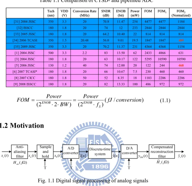
1.2 Motivation
) (t xc xa(t) ) (jΩ Haa ) ( 0 t x xˆ n[ ] yˆ n[ ] yDA(t) ) ( ~ Ω j Hr ) ( ˆ t yrFig. 1.1 Digital signal processing of analog signals
Fig. 1.1 demonstrates the traditional Nyquist-rate ADCs operation in a DSP system. Compared with Nyquist-rate ADC, over-sampling ΣΔ ADC trades digital signal processing complexity for relaxed requirements on the analog components, so the advance digital CMOS process can be fully utilized. Moreover, CT ΣΔ ADCs exhibit an inherent anti-alias filter function, thus the power-hungry high performance anti-alias filters can be avoided, resulting a low-power DSP system implementation. These unique features are important for mobile applications such as wireless communications or instrument, since these are battery powered and limited in available space. Due to the non-sampling loop filter, it is feasible to build high-resolution CT ΣΔ ADCs with a BW up to MHz at the same time, leading to more
resolution at low power consumption, the popularity of CT ΣΔ ADCs has been growing.
Table 1.2 compares DT- and CT ΣΔ ADCs, and we can find out that: First, the inherent anti-aliasing characteristics of CT ΣΔ ADCs avoid using a power-hungry front-end filter, hence reduce the power consumption of the whole system. Second, the bandwidth requirement of operational amplifiers in CT filter is much lower than that in DT ones, so CT ΣΔ ADCs can apply for high speed operation easily, and provide high DR as well; but for the CT filters which employ absolute value of passive device to map the filter coefficients, the matching of device element (resistor and capacitor) could be a large uncertainty. Otherwise, more accurate and low-jitter sampling clock is required for CT ΣΔ ADCs driving, or the whole system may be unstable and the operation will be failed.
Table 1.2 Comparison of DT- and CT-ΣΔ ADCs
DT ΣΔ ADCs CT ΣΔ ADCs
Input signal Sampled signal Continuous signal
Signal BW ~a few 10 KHz ~a few 10 MHz
OSR Relatively high Relatively low
Loop filter type Switched-capacitor CT loop-filter
Settling requirement Critical Relaxed
Sampling frequency <100-150 MHz >400 MHz
Anti-aliasing Need extra filter Inherent filter
Coefficients mismatch Very good (0.1%) Worse (30%)
digital decimator (Fig. 1.2(a)). According to multi-channel real-time bio-signals monitoring system (Fig. 1.3) requirements, the thesis proposes a CMOS CT ΣΔ modulator (CTSDM) with 10 MHz signal bandwidth and 12 effective number of bit (ENOB). By combining the over-sampling technique and blackened signal processing, a single SDM is utilized to sample 1024 signals from an electrode array with the signal bandwidth of 9 KHz for high frequency EEG detections. The target performance also promotes CT ΣΔ ADCs as alternative to other types of ADCs for wireless communications and medical imaging requirements. For the higher requirements of next generation applications in the future, the possibility of building CT ΣΔ ADCs will arise more by applying modern CMOS technology and new circuit technique (Fig. 1.2(b)).
(a) (b)
Fig. 1.2 (a) Sigma-delta ADC block diagram (b) Bandwidth resolution tradeoffs
... ... ...
Fig. 1.3 Multi-channel real-time bio-signals monitoring system
Sigma-delta modulator
Decimation filter
Analog input Digital output Sigma-delta ADC This work Discrete-time Sigma-delta Successive Approximation Subranging, Pipelined Continuous-time Sigma-delta Flash Signal Bandwidth Converted
1.3 Thesis Organization
This thesis covers theoretical analysis of CTSDM and practical circuit design implementation. After introducing the fundamentals of ΣΔ modulator, the design challenge of CTSDM is discussed. According to the target specifications of the CTSDM, the design procedure from system level to transistor level is detailed. The transistor level simulation and prototype chip measurement are also presented. The thesis is organized as following:
Chapter 1 consists of simple introduction and motivation of this thesis.
Chapter 2 is an overview of general ΣΔ modulator. The fundamental of A/D conversion is introduced briefly, such as sampling and quantization. The principles of oversampling and noise shaping are also described. Furthermore, advance techniques such as multi-stage or multi-bit ΣΔ modulator are introduced, which can achieve higher resolution. Finally, the basic CTSDM architecture is introduced, and the inherent anti-alias filter function is also discussed.
In Chapter 3, some main design issues of CTSDM are considered. Here discusses the non-idealities of CT integrator, including finite gain and unity gain bandwidth of the amplifier. The variation of filter time constant is also covered. After them, the excess loop delay problem is introduced, and some solution of prior work is described. The clock jitter effect is presented finally, which may cause the degradation of the resolution of whole modulator.
Chapter 4 proposes the system level design procedure. Due to the CMOS process limitations and reliability, the system level parameters must be designed carefully. For such a high speed applications, appropriate modulator architecture is very important.
modified form ideal value. The system simulation result of overall modulator is presented in the last part.
In Chapter 5, practical circuit design and implementation is introduced. Some non-idealities of practical circuit implementation are considered. The building block designs of proposed CTSDM are detailed. Finally, the transistor level simulation of CTSDM is presented.
Chapter 6 covers the test environment and the experimental result. Chapter 7 concludes the thesis and discusses some future work.
Chapter 2
Fundamentals of ΣΔ Modulator
_________________________________________
In this chapter, the basic concepts of ADC are introduced, including sampling and quantization. Then the fundamentals of ΣΔ ADCs are illustrated, the over-sampling and noise-shaping techniques are described. Above introduction about general ΣΔ A/D conversion is based on [21]. For high speed applications, multi-stage or multi-bit modulator architecture is often used to achieve higher SNR. Finally, the CTSDM topology is introduced. The inherent anti-aliasing filtering effect of CTSDM is presented by an example.
___________________________________________________
2.1 Sampling and Quantization
Analog to digital conversion is described in terms of two main operations: sampling in time domain, and quantization in signal amplitude. In the sampling
process, a analog continuous-time signal is sampled at a unit time interval,T , S
resulting the discrete sampled signal, which can be represented asx[n]=x(nTS). The effect of sampling process in the frequency domain is to create periodically repeated
versions of the signal spectrum at multiples of the sampling frequency fS =1/TS,
which can be written in Eq. 2.1:
∑
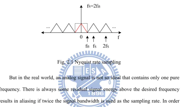
∞ −∞ = − = k S S S X f kf T f X ( ) 1 ( ) (2.1)Assuming the sampling frequency is twice the signal bandwidth, as shown in Fig. 2.1, then the repeated signal spectrum will not overlap in frequency domain exactly, and this signal can be perfectly reconstructed back to continuous time. In other words,
a signal with bandwidth fB must be sampled at a rate greater than twice the
bandwidth, fS ≥2fB, which is known as Nyquist rate theorem.
Fig. 2.1 Nyquist rate sampling
But in the real world, an analog signal is not so ideal that contains only one pure frequency. There is always some residual signal energy above the desired frequency results in aliasing if twice the signal bandwidth is used as the sampling rate. In order to avoid this problem, an anti-aliasing filter is often used to ensure that the signal is indeed band limited to half the sampling frequency. However, the analog anti-aliasing filter preceding the sampler must have very sharp cutoff frequency characteristic, which is very power- and area- hungry.
Once sampled, the signal must be quantized to a finite set of output values, and the quantized output amplitudes are usually represented by a digital code word composed of a finite number of bits. In Fig. 2.2, a 1-bit ADC example is shown. If the input signal (x axis value) is greater than 0, than it is quantized to output level V (y axis value), which is mapped to digital code “1.” On the other hand, the ADC output will be -V if the input is smaller than 0, and the mapping digital code is “0.”
V -V
y
x 0
Fig. 2.2 1-bit quantization
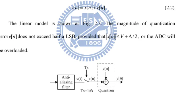
For the tractable analysis of the ADC, the behavior of quantization can be modeled as a linear noise source. Here defines the least significant bit (LSB) of an
ADC with Q quantization levels is equivalent toΔ=2V/(Q−1). The quantization
error can be represented as an additional noise source, and the output of ADC is shown as: ] [ ] [ ] [n xn en y = + (2.2)
The linear model is shown as Fig. 2.3. The magnitude of quantization errore[n]does not exceed half a LSB, provided thatx[n] ≤ V+Δ/2, or the ADC will
be overloaded.
Fig. 2.3 Block diagram and model of a conventional ADC
In general, the quantization error is a white noise process. Consider an N bit
ADC with N
Q=2 quantization levels, i.e., withΔ=2V/(Q−1)=2V/(2N −1). For a
zero meane[n], its varianceσe2or power is:
12 / ) 2 2 ( ) 1 2 2 ( 12 2 2 2 2 N N e V V ≈ − = Δ = σ (2.3)
If the signal is treated as a zero mean random process and its power isσx2, then the signal to quantization noise ratio is:
) ( 02 . 6 77 . 4 ) log( 10 ) log( 10 2 2 2 2 dB N V SNR x e x = + + = σ σ σ (2.4)
Thus, for each extra bit of resolution in the ADC, there is about 6 dB improvement in the SNR. For a sinusoidal input, the dynamic range of the ADC is
defined as the ratio of the signal power of a full scale sinusoid ( 2/2
V ) to the signal
power of a small sinusoidal input that results in a SNR of 1 (or 0 dB,Δ2/12). The
dynamic range expression and the result value is:
) ( 76 . 1 02 . 6 ) 12 ) 2 / 2 ( / 2 ( ) 12 / 2 ( 2 2 2 2 dB N DR V V V N + = ≈ Δ (2.5)
The value of Eq. 2.5 is just the peak SNR of the ADC for a sinusoidal input, i.e., the dynamic range of the Nyquist rate ADC is the same as its peak SNR.
2.2 Oversampling
Oversampling analog-to-digital conversion is a technique that improves the
resolution obtained from traditional Nyquist-rate conversion. The improvement is achieved by sampling the signal with a sampling rate which is much faster than Nyquist rate. As shown in Fig. 2.2(a), the same noise power in Nyquist rate case has
been spread over a bandwidth equal to the sampling frequency, fS, while this sampling
frequency is much greater than the original signal bandwidth, fB. Thus, only a small
fraction of the total noise power falls in the range between -fB and fB, and the
Fig. 2.4 Quantization noise power spectral density for oversampled conversion After the digital low-pass filter, the signal will be downsampled to the Nyquist rate. The operation of digital low-pass filtering and downsampling is called decimation, and the block diagram of the oversampling ADC model can be shown as Fig. 2.5.
Fig. 2.5 Oversampled conversion system
Assuming that the back-end digital filter is ideal, then the in-band noise power σey2 of the ADC output is:
) 2 ( 2 ) ( 2 ) ( 2 0 2 0 2 S B e f S e f ey f f ey ey f f df f df f P df f P B B B B σ σ σ =
∫
=∫
=∫
= − (2.6)The maximum achievable SNR is:
) ( ) 2 log( 10 ) log( 10 ) log( 10 ) log( 10 2 2 2 2 dB f f SNR B S ey x ey x = − + = σ σ σ σ (2.7)
Here define the oversampling ratio (OSR) as 2r
=fS/2fB, Eq. 2.7 can be expressed
) ( 01 . 3 ) log( 10 ) log( 10 ) log( 10 2 2 2 2 dB r SNR x ey ey x = − + = σ σ σ σ (2.8)
From Eq. 2.8, for every doubling the oversampling ratio r, the SNR of the ADC improves by about 3 dB (0.5 bit resolution). It means that to achieve the same SNR compared with Nyquist rate ADC, the resolution of internal quantizer in oversampling ADC can be much lower than that of the overall conversion resolution, i.e., the analog circuit complexity is simplified by oversampling the signal.
In addition, due to the oversampling technique, the front-end analog anti-aliasing filter does not need a very sharp cutoff frequency. For example in Fig. 2.6, the signal is sampled at four times the signal bandwidth. Here, the anti-aliasing filter can have a transition band between fB and fS/2, while it still attenuate the out-of-band noise power
very well. The design effort in analog circuit can be relaxed more. Sampling at four times the
signal bandwidth fS=4fB 0 ... ... fB fS 2fS f
Fig. 2.6 Oversampling ADC example
2.3 Noise Shaped ΣΔ Modulator
In general, the z-domain output of an ADC can be written as: ) ( ) ( ) ( ) ( ) (z X z H z E z H z Y = x + e (2.9)
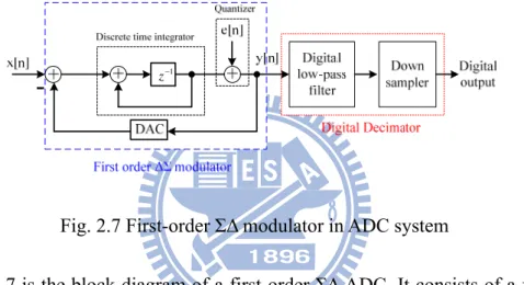
function (NTF). For oversampled ADC, He can be designed to be different fromH . x NTF can be modified, which attenuates the in-band noise and amplifies it outside the signal band. The technique is the so called noise shaping or modulation. Just like the oversampled ADCs, the modulator output then is low-pass filtered and finally is downsampled to the Nyquist rate. By oversampling and noise shaping, ΣΔ ADC can achieve very high resolution with relaxed analog circuit requirements, while the price of the improvement in SNR is the increased complexity of the digital hardware.
1 −
z
Fig. 2.7 First-order ΣΔ modulator in ADC system
Fig. 2.7 is the block diagram of a first-order ΣΔ ADC. It consists of a front-end modulator and following a digital decimator. The analog modulator covers an integrator, a quantizer and a digital-to-analog converter (DAC).If the DAC is ideal,
the z-domain modulator outputY(z)is given by:
) 1 )( ( ) ( ) ( = −1+ − −1 z z E z z X z Y (2.10)
The STF is z-1 and the NTF is (1-z-1) in Eq. 2.10. In ΣΔ ADCs, it is common to use
1-bit DAC and a corresponding 1-bit quantizer for the perfect linearity. And the total in-band noise power of the modulator is:
3 2 2 2 ) 2 ( 3 S B e ey f f π σ σ = (2.11)
The SNR in dB is: ) ( ) 2 log( 30 ) 3 log( 10 ) log( 10 ) log( 10 ) log( 10 2 2 2 2 2 dB f f SNR B S ey x ey x = − − + = σ σ π σ σ (2.12)
With OSR defined as 2r
=fS/2fB, we obtain: ) ( 03 . 9 ) 3 log( 10 ) log( 10 ) log( 10 ) log( 10 2 2 2 2 2 dB r SNR x ey ey x = − − + = σ σ π σ σ (2.13)
From Eq. 2.13, for every doubling the oversampling ratio r, the SNR of the ADC improves by about 9 dB (1.5 bits resolution).
+
+
1 − z+
x[n] e[n] y[n] DAC Discrete time integratorQuantizer
+
+
Discrete time integrator
1 −
z
Fig. 2.8 Second-order ΣΔ modulator
Then we consider a second-order ΣΔ modulator, which is widely used in many applications. In Fig. 2.8, the modulator realizes STF is z-1 and NTF is (1-z-1)2, the
output Y(z) is:
2 1 1 ( )(1 ) ) ( ) (z =X z z− +E z −z− Y (2.14)
Compared with first-order ΣΔ ADC, the second order NTF provides more quantization noise suppression in the signal band and pushes more this noise power to high frequency which is out of band. Again assuming that the second-order ΣΔ modulator output is filtered by an ideal low-pass filter, the in-band SNR is given that:
) ( ) 2 log( 50 ) 5 log( 10 ) log( 10 ) log( 10 ) log( 10 2 2 2 2 2 dB f f SNR B S ey x ey x = − − + = σ σ π σ σ (2.15) Letting 2r =fS/2fB, we obtain: ) ( 05 . 15 ) 5 log( 10 ) log( 10 ) log( 10 ) log( 10 2 2 2 2 2 dB r SNR x ey ey x = − − + = σ σ π σ σ (2.16) From Eq. 2.16, for every doubling the oversampling ratio r, the SNR of the ADC improves by about 15 dB (2.5 bits resolution).
Finally, we discuss a standard Lth-order ΣΔ modulator based on the extension of the first and second order ones. By realizing higher order NTF, ΣΔ modulator can push more quantization noise outside the signal band and attenuate the in band noise more, thus the higher SNR can be achieved. In other words, the same resolution can be achieved by a lower sampling rate combined with a high order ΣΔ modulator. Thus, the speed requirements on the analog hardware can be relaxed.
The Lth-order NTF is given by (1-z-1)L, and the STF is z-1. The ideal in-band
SNR achieved by the Lth-order modulator is :
) ( ) 2 log( ) 10 20 ( ) 1 l 2 log( 10 ) log( 10 ) log( 10 ) log( 10 2 2 2l 2 2 dB f f L SNR B S ey x ey x + + + − − = = σ σ π σ σ (2.17) From Eq. 2.17, for every doubling the oversampling ratio r, the SNR of the ADC improves by about (6L+3) dB (L+0.5 bits resolution). However, unlike first- and
second-order modulator, high order filter do face the stability problem. The quantizer of the modulator could overload due to the saturation of the integrator output. This is a main concern of designing high order modulator.
2.4 Multi-Stage and Multi-bit ΣΔ Modulator
From above discussion, high order ΣΔ modulator can achieve higher SNR but also suffers from stability problem. In additional to single-loop architecture, high order noise shaping can be realized by cascading independent modulator stages.
1 1 1 − − − z z 1 1 1 − − − z z 1 1 1 − − − z z 1 1 1 − − − z z 2 − z 2 1) 1 ( − z−
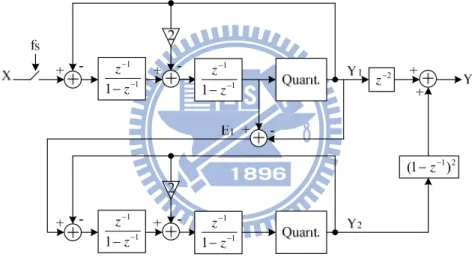
Fig. 2.9 Example of 2-2 cascaded DT ΣΔ modulator
For example in Fig. 2.9 [3], the output of the first modulator stage is connected to the second modulator input, the expression of Y1(z) and Y2(z) is:
2 1 2 1 2 2 2 1 1 2 1 ) 1 )( ( ) ( ) ( ) 1 )( ( ) ( ) ( − − − − − + − = − + = z z E z E z z Y z z E z X z z Y (2.18)
To obtain the final output Y(z), the Y1(z) and Y2(z) are passed through a digital delay
(z-1) and a digital differentiator (1-z-1) first, then the sum result of Y
1 and Y2 is : 4 1 2 4 ( ) ( )(1 ) ) ( = − + − − z z E z X z z Y (2.19)
Finally, the fourth-order quantization noise suppression can be achieved by cascading two single-loop second-order ΣΔ modulators. This implies that the SNR of the cascaded modulator is as high as single loop fourth-order modulator, and the system is guaranteed to be stable the same time. This is the main advantage of the cascaded (or multi-stage) ΣΔ modulator topology.
However, the cascaded structure requires perfect matching between analog and digital transfer function. Otherwise, the quantization noise of first-stage modulator can not be cancelled completely, which may cause significant degradation in overall SNR. Generally, extra calibration circuit must be designed to compensate the mismatch for avoiding this problem.
So far, aforementioned discussions focus on the ΣΔ modulators with only one-bit internal quantizer and DAC. In fact, multi-bit quantization is widely used to achieve even higher resolution. From Eq. 2.5, it is easy to see that for each additional bit used in the internal quantizer, the 6 dB improvement in SNR can be obtained. The behavior of a multi-bit ΣΔ modulator system is more closed to the linear model of quantization noise, and the stability of high order loop modulator using multi-bit quantization is more accurately predicted. Thanks to this technique, the sampling rate can be reduced while keeping the resolution the same, and the speed requirement of analog circuit is relaxed more. Nevertheless, the linearity of the multi-bit DAC in VLSI is a main issue while applying multi-bit ΣΔ modulators. To achieve sufficient linearity needed for high resolution conversion, digital dynamic element matching (DEM) or additional calibration circuits are used. Moreover, multi-bit digital output of the modulator complicates the digital low-pass filter design, and the hardware cost is increased in digital circuit.
2.5 Continuous-time ΣΔ Modulator
H(s) DAC Analog input Digital output sampler+
-Loop filter Ts Quantizer
Ts
Fig. 2.10 Conventional CTSDM block diagram
Compared with discrete-time architecture incorporating switch-capacitor circuits, more ΣΔ modulator implementations employing continuous-time loop filter have been presented in recent years. A simple CTSDM block diagram is show in Fig. 2.10, which comprises a continuous-time loop filter, a quantizer and a feedback DAC. Traditionally, the maximum sampling frequency which discrete-time ΣΔ modulators can achieve is limited to the operational amplifiers (opamps) requirement. To reduce the settling error and distortion in switch-capacitor circuit, the sampling rate must be as high as five times the gain-bandwidth product (GBW) of the opamps. For CTSDM, this requirement can be relaxed. According to [16], GBW in continuous-time integrators can be as low as sampling frequency without significant degradation of SNR. In other words, CTSDM is more suitable for high speed operation compared with discrete-time one. Besides, due to the non-sampling input stage, CTSDM exhibits an inherent anti-alias filter function.
Σ τ s 1 DAC ) ( ˆ t u fS=1/TS ) ( ˆ t x x(n) y(n) ) ( ˆ t y Fig. 2.11 First-order CTSDM
In Fig. 2.11, a first-order low-pass CTSDM is shown as a simple example [16]. The modulator compromises a single continuous-time integrator, a comparator (1-bit quantizer) and a corresponding 1-bit non-return-to-zero (NRZ) DAC. The quantizer input expression in time domain can be obtained:
dt t u n y T n x n x S S T n nT S +
∫
+ − = +1) ( ) ( ) 1 ( 1) ˆ( ) ( τ τ (2.20)The input signal uˆ t( ) will be integrated over one clock (TS) before sampling, and the
input integral can be written as:
) / ( sin ) ( ˆ ) ) 1 ( , ( ) ( ˆ ) ( ˆ ) 1 ( S S S T n nT u t dt u t rect nT n T U s c f f S S ⋅ = + ∗ =
∫
+ (2.21)Consequently, the input spectrum is multiplied by a sinc function, which has spectral
nulls at frequencies±αfS,α ≥1. In CTSDM, the anti-aliasing property just arises
because the sampling happens after the integrator, while the order of the anti-aliasing filter will be increased as well as that of the modulator. Therefore, a high cost analog front-end filter can be avoided in whole ADC system. Above these discussions, continuous-time ΣΔ ADC can achieve high resolution and high speed operation at the same time. Compared with pipelined or subranging type converters, this approach can be more power- and area-efficient for the equivalent SNR and bandwidth,
Chapter 3
Design Issues of CT ΣΔ Modulator
_________________________________________
While realizing the CTSDM with practical circuits, the non-idealities of the analog blocks must be considered. These effects may influence the performance of the modulator as well as the stability of the whole system. In this chapter, the main design issues of CTSDM are discussed, covering the non-idealities in CT integrators, excess loop delay and clock jitter. Especially in high speed operations, these errors could degrade the SNR achieved by the modulator significantly. In recent years, many related discussions and compensation methods are presented.
_____________________________________________________________________
3.1 Non-idealities of CT Integrator
Fig. 3.1 Commonly used CT integrator
The commonly used CT integrators are active-RC integrators and Gm-C integrators, as shown in Fig. 3.1. RC integrators combine passive device with opamp
output experience very small signal swing, resulting in very good linearity. On the contrary, Gm-C integrators operate under open-loop condition, and the linearity will be decreased due to the large swing of the input. The main advantage of Gm-C ones is the achieved bandwidth can be relative high. The power consumption will be lower than RC integrators for the same speed requirement.
When the RC integrators are employed to build CTSDM, the virtual ground provided by the closed-loop opamp applications can greatly increase the linearity of the feedback DAC whose output is connect to the input of opamp. For Gm-C integrators, the linearity of DAC will be decreased due to the large swing of the integrator output, which is directly connected with DAC output. According to the above analysis, hybrid integrators have been used for the different requirement in multi-stage loop filters [1]. Here, the active-RC integrators are preferred for its good linearity and reasonable power consumption with the target speed requirement, so only the non-idealities of the RC integrators will be discussed.
3.1.1 Leaky CT Integrator
In CTSDM, the first integrator is the most critical and main power-consuming circuit of whole system. Because any errors of this integrator will add to the modulator input directly, the performance of the ADC will be degraded seriously. Thus, its specification requirements should be considered in detail according to the trade off between distortion and power consumption.
First, the dc gain of opamp is discussed. Unlike ideal opamp which has infinite dc gain, the finite gain of real opamp will cause additional parasitic pole in CT integrators. The practical transfer function of the CT integrator due to this effect can be expressed as [13]:
0 0 0 0 1 , 1 ) 1 ( 0 A f A A s f A s I I A + = + = + + + γ α γ ε (3.1)
A0 represents the finite dc gain of the opamp, and fI is the inverse of the
integrator time constant. α and γ represent the integrator gain error and the pole
displacement. In order to minimize the degradation in SNR due to this non-ideality, the gain requirement can be obtained by computing the in-band noise effect. From [13], the critical gain of a third-order CTSDM is :
π ζ ζ OSR A dB ) 1 10 ( 5 21 10 0 − ≈ (3.2)
ζ represents the loss of the SNR while only leakage is considered. If other
distortion and noise are taken into account also, the required dc gain has to be much higher than Eq. 3.2.
3.1.2 Finite Gain Bandwidth of Opamp
1
1
-+
o
n
n
) (s Athe transfer function of the amplifier is given byA(s). Thus, one can calculate that the output of this integrator can be expressed as [17]:
∞ → ≈ + + =
∑
= ) ( , ) ( 1 ) ) ( 1 1 ( ) ( 1 s A s f k f k s A s A s f k s ITF i I N l l I I i i (3.3) ik denotes the scaling coefficient of the ith integrator. Compared with ideal
opamps, the dc gain and the gain bandwidth product of a real opamp are finite, resulting in an additional non-dominant pole in integrators. This will degrade the loop stability of the entire modulator by pushing the poles closer to the imaginary axis. The transfer function of a real opamp comprises a finite dc gain and several poles and zeros. Taking the influence of finite gain bandwidth into account, the behavior of the simplified non-ideal amplifier can be expressed as:
] / [ , 1 ) ( GBW A rad s s A s A dc A A dc ω ω = + = (3.4) A
ω is the dominant pole of the amplifier inside the integrator, and A represents dc
the finite dc gain. Incorporating Eq. 3.4 into Eq. 3.3, the entire transfer function is:
s p GBW s i l l s l l s s i i s GBW f GBW c s GE s f k f k GBW s f k GBW GBW s f k ITF π ω 2 1 1 | | | | | ) ( = + = + + + ≈
∑
∑
(3.5)As a rule of thumb, c=2 is a conservative chose that performance loss is negligible and the amplifier do not waste much power at the same time. In CTSDM, some papers found that the GBW could even be as low as sampling frequency.
Fig. 3.3 Non-dominant pole cancellation
In order to cancel the parasitic pole, a resistor rz can be added in front of the
integration capacitor. As shown in Fig. 3.3, the value of this resistor is [26]:
C GBW r sRC sCr ITF z z ⋅ ≈ → + = 1 1 (3.6)
3.1.3 RC Time Constant Variation
Because the transfer function of CT integrators is related to the RC time constant which can vary largely due to the process variation and temperature, this non-ideality becomes a challenge in CTSDM design. In modern CMOS technology, the absolute value of resistors and capacitors can vary as large as 10-20%, thus the resulting integrator gain error could be more than 30%. For a real CT integrator, the RC time
constant variation can be considered asΔ in transfer function, which can be RC
expressed as [17]: s f k GE k s f C sR ITF i I RC i I RC i RC = Δ + = Δ + = ) 1 ( ) 1 ( 1 (3.7) The effect of RC time constant can be observed form system simulation incorporating Eq. 3.7 as a non-deal model. Generally, the result will be like Fig. 3.4, which is just an example diagram:
SNDR V.S. Normalized Time Constant
70
75
80
85
90
0.5
0.6
0.7
0.8
0.9
1
1.1
1.2
1.3
1.4
1.5
Normalized Time Constant (Ts)
S
NDR
(
dB
)
unstable
Fig. 3.4 SNDR V.S. time constant variation
The normalized RC time constant is set to be 1 in Fig. 3.4. When the RC tine constant is smaller, a better SNR can be obtained due to the higher gain of loop filter. However, the modulator could be unstable when the gain becomes too larger. On the other hand, a RC time constant is larger than 1 will lead to a more stable modulator, but the achieved SNR will decrease due to the less efficient noise shaping. To compensate this variation, a convenient method can be used by implementing the integration capacitor with tunable capacitor array [1]. As shown in Fig. 3.5, the number of digital control word bit can be designed according to the tuning accuracy requirement.
Fig. 3.5 Tunable capacitor array
3.2 Excess Loop Delay
In practical circuit implementation, the speed of transistors is infinite. It means that the delay between sampling clock and circuit output is non-zero. This delay, which is known as excess loop delay, usually consists of quantizer, DAC and loop filter delay. Sometimes, dynamic element matching technique will be employed to enhance the linearity of the multi-bit DAC. However, this extra signal processing will lead to more serious problem.
In general, there are two types of impulse response for feedback DAC output. In Fig. 3.6, return-to-zero (RZ) and non-return-to-zero (NRZ) pulse shaping including the excess loop delay (td) are shown:
hRZ(t)
0 td Ts/2+td Ts t
hNRZ(t)
0 td Ts/2 Ts Ts+td t
order of the DT loop filter equivalent to CT one will be higher by one, and the modulator will be unstable. Moreover, excess loop delay could also degrade the effect of noise shaping as well as SNR and dynamic range of modulator. Traditionally, the RZ pulse shaping can be used to relax the excess loop delay. As shown in Fig. 3.6, if the delay is smaller than half the sampling clock period, then the falling edge of DAC pulse is indeed within the range between Ts/2 and Ts, and the order of the equivalent DT loop filter is the same as CT one. Nevertheless, for very high sampling frequency in wideband CTSDM, RZ pulse shaping is more sensitive to clock jitter than NRZ one. Recently, the common solution to the excess loop delay is to use NRZ DAC pulse incorporating an explicit full clock delay in the feedback path. Thus, the varying quantizer delay and other delays caused by digital logic circuit can be absorbed. Besides, in order to compensate the response sample in the CT loop filter, an extra feedback branch will be added directly to the quantizer input to make the impulse response of CT loop equivalent to DT one [1].
3.3 Clock Jitter Influence
In CTSDM, there are two points in Fig. 2.10 where sampling clock jitter will occur and affect the performance of the modulator. First, the sampling error due to the clock jitter in quantizer input will be suppressed due to the high gain of the noise shaping filter, hence the SNR degradation could be negligible. However, the sampling uncertainties of the feedback DAC will produce errors into the modulator input at every sampling instant. These timing errors will appear at the modulator without any attenuation, which may cause the performance degradation of the whole system directly. Thus, the DAC clock jitter is one of the most important issues that should be considered carefully while designing wideband CTSDM.
area. The equivalent additive errors can be expressed as [2]: T n T n y n y T n A n e n T n y n y n A DAC j DAC ] [ ]) 1 [ ] [ ( ] [ ] [ ] [ ]) 1 [ ] [ ( ] [ Δ ⋅ − − = Δ = Δ ⋅ − − = Δ (3.8) ] [n TDAC
Δ is the DAC sampling uncertainty and T is the ideal sampling clock
period. According to [2], Eq. 3.8 can be utilized in system simulation model to observe the effect of clock jitter noise, and the requirement of the rms clock jitter can be predicted for the whole system, as shown in Fig. 3.7. In [2], the modulator remains stable without significant SNR degradation up to a rms jitter of 30ps at a nominal sampling clock of 300 MHz. 1 1) 1 ( −z− T− ] [n TDAC Δ ] [n ej
Fig. 3.7 Clock jitter model for feedback DAC
NRZ DAC I , Δ NRZ DAC I ,
Fig. 3.8 Clock jitter in different types of DAC pulse shaping
In order to reduce the clock jitter sensitivity, multi-bit NRZ DAC pulse shaping is widely used instead of traditional RZ one. To ease the analysis of the jitter noise, one can assumes that the noise introduced by the clock jitter is a white noise spectrum.
same area of the output waveform, the amplitude of RZ DAC pulse is twice the NRZ DAC output. As the analysis in [1], the SNR improvement of NRZ pulse shaping over RZ pulse shaping can be derived:
dB SNR NRZ DAC NRZ DAC I I RZ NRZ ) 8 ( log 10 , , 2 2 10 Δ − ⋅ = σ σ (3.9) where IDAC,NRZ 2
σ is the variance of the NRZ DAC output current, and IDAC,NRZ
2 Δ
σ is the
Chapter 4
System Level Design
_________________________________________
In this chapter, the system level design of the proposed CTSDM is described in detail. The top-to-down design flow is introduced, and many system level considerations are discussed, which include the system level parameters, the architecture of the modulator, the loop filter coefficients. In the last part, the overall system simulation is shown.
_____________________________________________________________________
4.1 System Level Parameters
As described in chapter 1, the target resolution of the proposed CTSDM is 12-bit ENOB with 10 MHz signal bandwidth. Once the specifications of the modulator are decided, the system parameters must be designed carefully to achieve these targets. The ENOB and the corresponding peak SNR (the same as dynamic range) of a SDM can be calculated by the following equation:
02 . 6 76 . 1 − =DR ENOB (4.1) 1 2 2 2 )(2 1) 1 2 ( 2 3 + − × + = N L L OSR L DR π (4.2)
The system parameters in Eq. 4.2 [2] include the resolution of internal quantizer (N), the loop filter order (L) and the oversampling ratio (OSR).
overdesign specification to 14-bit ENOB (peak SNR = 86 dB), then the decision of the above system parameters is discussed as following: first, one can start from the OSR, which is related to the operating speed of the modulator. Because the target signal bandwidth is as high as 10 MHz, taking the 0.18-μm CMOS process limit and the trade off between GBW and power consumption of opamp into account, a sampling rate of 500 MHz is a reasonable upper bound [8]. In addition, OSR is usually a power of two to simplify the back-end decimation filter design, so the OSR can be 2, 4, 8, 16 or 32 (corresponding sampling rate is 640 MHz). In [8], an OSR smaller than 10 implies that the GBW of the opamp must be high enough than the situation that OSR larger than 10 to provide the loop gain for linear operation. Based on the above discussion, an OSR of 16 (sampling rate is 320 MHz) is an appropriate choice for the modern CMOS process limitation. Second, the loop filter order can be considered for the modulator stability and design effort. A filter order larger than 3 may cause the quantizer overloaded easily and result an unstable system. Moreover, high order loop filter means that the number of the corresponding system coefficients is much more than the low order one, which may complicate the system design. Third, due to the relatively lower OSR in CTSDM than in DT one, multi-bit quantizer is commonly used to achieve the same SNR. Finally, it can be seen that a loop filter order of 3 combined with a 4-bit quantizer is a suitable solution in considering the modulator stability and the achieve performance. With OSR = 16, L = 3 and N = 4 in Eq. 4.2, the resulted peak SNR is 88.19 dB, which is larger than the target specification.
4.2 CT ΣΔ Modulator Topology
As introduced in chapter 2, the single-loop SDM is commonly used for its simple circuit design. Although cascaded or time-interleaved modulators have been presented in some early papers, additional noise cancellation filter or more chip area must be used for the practical implementation, and the circuit design becomes even more complicated. Compared with low-pass loop filter, band-pass and complex ones are employed in some specific applications ICs. But for the target signal bandwidth of 10 MHz, these topologies require much higher GBW in the amplifiers, which are not so power-efficient. So, the proposed CTSDM focuses on a single-loop, low-pass topology.
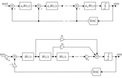
4.3 Architecture of the Loop Filter
In general, there are two types of the loop filter architectures to form the CTSDM system: cascade of integrators (CI) combined with distributed feedback (FB) or feed-forward (FF) [17]. ) ( 1H z a a2H(z) aNH(z) ) (n u y(n) ) (z H ) (n u y(n) ) (z H H(z) 1 − sig a 1 a 2 a N a
contains a significant amount of the input amplitude, which implies that the integrator will operate at large output swing. In order to avoid the integrator overload, the system coefficients of loop filter must be designed carefully, which are usually smaller than CIFF topology. Smaller passive device in layout means that the matching could be a problem due to process variation. In contrast, CIFF (Fig. 4.1(b)) is more suitable for low power design because of the small swing of the integrator output. But the sum of the feed-forward path could cause overload in quantizer input, a peak transient response also occurs at high frequency of the signal transfer function (STF) at the same time. Combined with above discussion, the hybrid loop filter architecture is presented in [5], which covers the advantages of both CIFB and CIFF ones, and the additional summation circuit is also avoided.
Except for the common topologies in Fig. 4.1, a local feedback loop around pairs of integrators can move the zeros of noise transfer function away from dc and spread over the signal band. Consequently, the in-band SNR will be improved. Moreover, the excess loop delay issue of the CTSDM can be compensated by an extra feedback path, so a additional branch of feedback signal is added in front of the quantizer input. The whole proposed loop filter architecture is shown as Fig. 4.2, where k1, k2 and k3 represent the integrator coefficients, k4 is the feed-forward coefficient, kz denotes the local feedback path, kb1 and kb3 are feedback path, and kd is the compensation coefficient of the excess loop delay.
s sT 1 s sT 1 s sT 1
Fig. 4.2 Combination of FF and FB architecture CTSDM
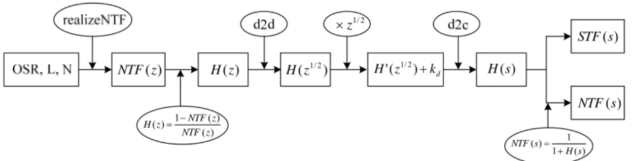
4.4 Loop Filter Coefficients
According to [5], the coefficients of continuous-time loop filter can be derived by MATLAB and delta-sigma toolbox [27][28]. The overall flow is shown as Fig. 4.3: first, substitute the system level parameters into the MATLAB toolbox, then the optimized NTF can be obtained according to [28]. By using the “d2d”
(discrete-to-discrete) function, an equivalent transfer function in z1/2 is derived. The
half sample delay (z-1/2) of the quantizer can be incorporated by multiplying (z)
H with
z1/2. Finally, the equivalent continuous-time transfer function in s-domain can be
obtained. ) (z H H'(z )+kd 2 / 1 ) (z NTF H(s) ) ( ) ( 1 ) ( z NTF z NTF z H = − ) (s STF ) (s NTF ) ( 1 1 ) ( s H s NTF + = ) ( 1/2 z H 2 / 1 z ×
3 2 1 4 1 3 2 3 3 3 3 2 3 3 2 3 2 3 ) ( ) ( 6147 . 0 705 . 1 321 . 2 02401 . 0 ) ( 05593 . 0 3002 . 0 6323 . 0 1 977 . 2 977 . 2 ) ( ,4) NTF(3,16,1 synthesize k k k s k k k k s k s s k k s s NTF s s s s s s NTF z z z z z z z NTF b b z b z + + + + + = + + + + = ⇒ − + − − + − = ⇒ = (4.3) Eq. 4.3 is the final NTF in s-domain. Combined with this equation and Fig. 4.2, the loop filter coefficients can be chosen. The coefficients considerations are following: first, if the internal integration coefficient is larger than 1, the output of integrators will saturate easily. Second, because these coefficients correspond to the equivalent R-C time constant, considering the matching in practical circuit implementation, it is better to design these coefficients in a ratio relation, so the original coefficients must be modified. The proposed loop filter coefficients for Fig. 4.2 are shown as Table 4.1.
Table 4.1 Proposed loop filter coefficients for CTSDM (a) original (b) modified
k1 k2 k3 k4 Kz kb1,3 kd 9/4 0.4267 0.6403 0.7471 3/80 9/4, 2.321 0.9619 (a) k1 k2 k3 K4 Kz kb1,3 kd 9/4 3/8 3/4 3/4 3/80 9/4 9/8 (b)
4.5 System Level Simulation
From the above discussion and design considerations, the MATLAB simulink model of whole CTSDM is shown in Fig. 4.4. Fig. 4.5 shows the system simulation result according to the designed loop filter coefficients, and the ideal peak SNR of 88.50 dB (corresponding ENOB = 14.41) is achieved by the proposed third order CTSDM with 4-bit quantizer and an OSR of 16. The amplitude of the input sin wave is 0.4, and the signal bandwidth is 3.203125 MHz. The FFT size is 4096 points.
k2 k1 k3 k4 z 1 Unit Delay 320e6 s Transfer Fcn2 320e6 s Transfer Fcn1 320e6 s Transfer Fcn yout Signal To Workspace Signal Generator Scope6 Quantizer 3/80 Kz 320MHz 3/4 3/8 9/4 3/4 9/8 kd 9/4 kb3 9/4 kb1
Fig. 4.4 Simulink model of the proposed CTSDM
100 101 102 103 104 −150 −100 −50 0 Frequency [Hz] Output spectrum [dB]
Chapter 5
Circuit Design and Implementation
_________________________________________
After system level design and considerations, the practical circuit implementation of the proposed CTSDM must be designed carefully. First, the active RC architecture is considered, and the value of the equivalent resistors and capacitors must be determined according to thermal noise consideration. Then the corresponding building blocks of CTSDM are described, such as two-stage opamp, flash ADC and the feedback current-steering DAC. Clock generator and capacitor tuning circuit are used for the improvement of the SNR. In the last part, the transistor level simulation result is shown.
_____________________________________________________________________
5.1 Active-RC Integrator
5.1.1 Resistor and Capacitor Consideration
As introduced in Chapter 3, active RC integrator is chosen because of the high linearity and the high gain achieved by the opamp. Once the integrator topology is decided, the corresponding value of the resistors and capacitors must be designed according to thermal noise consideration. Owing to the three stages of integrator in the proposed CTSDM, the effect of induced noise and distortion form the second and
third integrators are attenuated by OSR2 and OSR4, which are negligible. In order to
target SNR, the maximum value of the usable resistors can be derived as following: the noise source of the first stage integrator is:
1 2
1 8 TRk
v
d in = B (5.1)
wherekBis Boltzmann constant, R1denotes the first integration resistor andT is the
absolute temperature. If the other noise of the circuit can be negligible, the total induced noise of the first stage can be expressed:
B B
noise k TR f
P ≈16 1 (5.2)
where fBis the signal bandwidth. Combined with Eq. 5.2 and the signal power of the
sin wave, the signal to thermal noise ratio must be larger than the signal to quantization noise, which may not affect the performance of CTSDM. The result is shown as: Ω = ≤ ⇒ ≥ = = = k SNR Tf k V R dB f TR k V f TR k V S S SNR B B SW B B SW B B SW N S 808 . 4 ) ( 32 0 . 74 32 16 2 2 1 1 2 1 2 (5.3)
whereVSW represents the signal swing, which is 0.4 here. According to Eq. 5.3 and
Table 4.1, the equivalent resistor and capacitor can be determined byki/TS =1/RC,
whereT is the period of sampling clock. Considering some design margin and S
practical implementation, the determined values are shown in Table 5.1. Table 5.1 Resistor and capacitor value of the proposed CTSDM
R1 R2 R3 R4 Rz C1,2,3
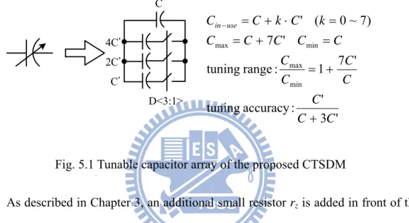
replaced by multiple capacitor array combined with MOSFET switch. Thus, the actual integration capacitor becomes tunable and the effect of process variation can be reduced. The circuit block diagram and the tuning range are shown in Fig. 5.1. According to TSMC 0.18 μm model, the proposed tuning range is sufficient to compensate ±30% resistor variation of real implementation.
Fig. 5.1 Tunable capacitor array of the proposed CTSDM
As described in Chapter 3, an additional small resistor rz is added in front of the
integration capacitor, which can compensate the influence of the finite GBW effect.
5.1.2 Two-stage Opamp
In CTSDM, the first stage integrator is the most important one because any noise and distortion in this stage is not attenuated by the loop filter, and this will cause significant degradation in SNR. For the resistive loading in continuous-time integrator, one stage opamp is not suitable due to the large output impedance. In [5], multistage opamp with nested Gm-C compensation (NGCC) is used, which can achieve very large gain (>80 dB). However, the frequency compensation of NGCC is very complex, and the multistage architecture may even waste some power consumption. From simpler design, two-stage Miller opamp structure is chosen, since it can provide high
' 3 ' : accuracy tuning ' 7 1 : range tuning ' 7 ) 7 ~ 0 ( ' min max min max C C C C C C C C C C C C k C k C Cin use + + = = + = = ⋅ + = − D<3:1> C 4C' 2C' C'
sufficient speed and gain requirements are found by MATLAB analysis. The used opamp structure and the corresponding continuous time common mode feedback (CMFB) circuit are shown in Fig. 5.2. For the same slew rate requirement, the calculated power consumption of NGCC [10] is 9.72 mW, while that of two-stage opamp is 7.92 mW. In other words, assuming that the power from opamp is 60% of whole modulator, the overall power consumption can be saved by 11% while replacing NGCC with two-stage opamp.
(a)
(b)