國立交通大學
電機學院 電子與光電學程
碩
士
論
文
使用二維低功耗移位控制解決方案在多個
掃描鏈設計的繞線實現
Routing Realization for Two-Dimension Low Power Shift Control
Methodology in Multiple Scan Chain Design
研 究 生:林秀銓 (Hsiu-Chuan Lin)
指導教授:陳宏明 教授 (Prof. Hung-Ming Chen)
使用二維低功耗移位控制解決方案在多個
掃描鏈設計的繞線實現
Routing Realization for Two-Dimension Low Power Shift Control
Methodology in Multiple Scan Chain Design
研 究 生:林秀銓 Student:Hsiu-Chuan Lin
指導教授:陳宏明 Advisor:Hung-Ming Chen
國 立 交 通 大 學
電機學院 電子與光電學程
碩 士 論 文
A ThesisSubmitted to College of Electrical and Computer Engineering National Chiao Tung University
in partial Fulfillment of the Requirements for the Degree of
Master of Science in
Electronics and Electro-Optical Engineering August 2009
Hsinchu, Taiwan, Republic of China
使用二維低功耗移位控制解決方案在
多個掃描鏈設計的繞線實現
學生: 林秀銓 指導老師:陳宏明國立交通大學 電機學院 電子與光電學程碩士班
摘要
隨著超大型積體電路進入到次微米製程,當積體電路在製造過程中是否有損壞的 測試上將面臨許多的挑戰。然而,在多條掃描線的測試方式下可以解決許多測試 問題,例如解決測試資料體積大小,測試時間和測試時的功率消耗等問題。再者, 利用二維掃描移位控制概念[21],我們可以容易實現在測試時的低功率消耗、測 試時間和測試資料大小以及讓這些方法在成電路時不佔用太多的晶片面積。在此 藍圖下,我們將可以忽略大量不需要測試的測試資料且不輸入至電路中做測試, 如此可以減少測試資料大小和測試時間。基於這個技術下,此篇論文所做的研究 將利用兩種群集方法[17]、[18]下去發展一個有效率的掃描順序,並且能實現在 實際的設計流程中。和比較傳統單一一條掃描線方式,在這裡所使用的兩種群集 方法,只要適度的調整繞線資源的使用率,此時並不會增大積體電路面積,因此 不會增加成本,當然還是會有代價的,就是-繞線會較為擁擠。因此,使用者可以 基於編碼效率或是在繞線擁擠度等客觀條件下,在這兩種群集方法下做最佳的選 擇並應用。Routing Realization for Two-Dimensional Low Power Shift
Control Methodology in Multiple Scan Chain Design
Student: Hsiu-Chuan Lin
Advisor: Hung-Ming Chen
Degree Program of Electrical and Computer Engineering
National Chiao Tung University
Abstract
The migration of VLSI design in submicron technologies has presented several challenges in manufacturing tests. Multiple scan chain schemes solve many testing issues, such as test data volume, test time and test power consumption. Based on a new two-dimensional scan shift control concept [21], we can achieve low test power with simpler implementation and smaller hardware overhead. This scheme skips many unnecessary don’t care patterns to reduce test time and test data volume. Based on this technique, this study applies two clustering approaches in [17] and [18] to develop an efficient scan ordering to achieve modern testing design flow. Compared with the traditional single scan chain, the two clustering approaches have little routing resource overhead. By adjusting the appropriate placement utilization rate within the routable region, the chip area is not increased, but with the price of routing congestion. Users may find a better tradeoff between the encoding efficiency, and routing congestion in both clustering approaches.
誌
謝
能完成這篇論文要感謝身邊的許多人。首先,要感謝指導教授陳宏明博士, 教授從旁適時地給予協助,並耐心地教導,讓我順利地完成學業。並感謝林佳毅 學長在研究方法和論文寫作上大力幫忙,並提供意見和指導,讓我能夠在掌握研 究大方向下得以完成此論文研究。還要感謝口試指導委員王俊堯教授、趙家佐教 授和溫宏斌教授的親臨指導,給我在研究上有近一步的啟發和認識。 其次,要感謝義隆電子陶逸欣處長和許文俊經理多年來,不管在工作上或是 課業上都給予最大的支持和包容讓我得以完成學業,還有廖建峰副理、林國鼎副 理、徐利君主任和陳志勝主任從旁給予協助和鼓勵,讓我得以學業和工作兩者兼 顧。
Contents
1. Introduction………... 1
2. Proposed Architecture: Two-Dimensional Low Power Shift Control Methodology………... 4
3. Clustering and Reordering Method………. 7
3.1 Uniform cluster area approach……….... 7
3.2 Uniform scan-cell number approach………... 8
3.3 Locating the scan-flip-flop in each cluster………... 10
3.4 Reordering………... 11
3.5 Implementing the modern design flow………... 12
4. Experimental Results……….. 14
4.1 Evaluation Phase... 15
4.2 Physical Phase………. 20
List of Figures
1. Proposed multiple scan chain architecture with 2-D 4x4 scan shift control chains. Combined with the proposed methodology, this test scheme
achieves low test power, small data volume, and short test time………….. 4 2. Design diagram of the proposed multiple scan chain architecture with
routing connection details………. 5 3. Circuit design of the proposed multiple scan chain architecture (a) is part
of the sub-scan-chain design and (b) presents the details for one scan
control chain……….. 5
4. Uniform cluster area approach. The area is identical, but the scan-flip-flop numbers are not equal in each cluster………... 8 5. Uniform scan-cell number approach, the scan-flip-flop number is identical
in all clusters except cluster C15. Since the test data contains many X-bits (don’t-care bits) and its pattern length does not need to be recorded during encoding, it contributes to more efficient and compact test patterns……… 9 6. Proposed modern design flow. To integrate the proposed testing scheme
into the design flow, we insert the two-dimensional scan-shift control circuits and shift-in pins into the design flow. Once ECO
placement-and-routing procedure is finished, the gate-level netlist is generated. The netlist through the ATPG tools generates the test patterns
to evaluate the whole design………. 13 7. (a) and (b) demonstrate the wire-length distribution in the
two-dimensional scan shift control structure for different types of scan-control lines on ISCAS’99 benchmark circuit b17. The unit of the
wire-length is μm……… 18
8. Reordering result of b17 circuit, the scan-control-1 and scan-control-2 are 4, respectively. (a) represents the uniform cluster area approach and (b) represents the uniform scan-cell number approach. The longer lines are the scan-control, shift-in and shift-out lines. These lines spread through the whole chip. The scan-control circuits are placed in the center of each
cluster by default………... 19
List of Tables
1. Circuit characteristics of ISCAS’89 and ISCAS’99 benchmark, showing the DFF, inverters and combinational gates, input pin and output pin
number………. 14
2. Wire-length results of ISCAS’89 and ISCAS’99 benchmark circuits by applying different numbers of clusters and implementing both
approaches, the uniform cluster area approach, and the uniform scan-cell number approach. The WLTotal is the sum of WL and SC WLCTRL
compared with the wire-length in both approaches………. 17 3. Physical routing result of the circuit b17 of ISCAS’99. The technology
process is UMC 0.18μm and 1P5M. The WLTotal represents the total
wire-length and the unit is in μm. The CTotal is the total contact number
and it also shows placement utilization for each circuit. Each circuit area is identical and the area is 633μm*628μm………. 20
Chapter 1
Introduction
The modern VLSI design process has migrated to nanometer technology. Gate-count numbers continue to increase. Transistor fabrication cost has reduced but testing cost has not been proportionally scaled. Since a large amount of test data volume is stored in ATE (Automatic Test Equipment), memory capacity should be enlarged to adopt these test data. Upgrading ATE involves extra cost. Compressing test data to reduce test time also reduces testing cost. Moreover, when test data shift-in, most devices switch at the same time. The power consumption in test mode is more than twice that in normal functional operation, and may cause chip failure, decrease reliability and reduce overall yield [1] [2].
The scan-based testing approach is widely applied, and one of the critical issues is that it can cause large power consumption instantly. Many different techniques reduce testing power and list in [3], such as scan cell reordering, scan chain segmentation and scan chain disabling. The multiple scan chain is one kind of scan chain segmentation, with shorter routing length than that of a single scan chain design [4], [5] and [6]. The multiple scan chain also evaluates many scan cells at the same time to reduce testing time. Moreover, a larger number of switching activities increase test power consumption, damaging the chip. To reduce testing power consumption, minimum transition fill (MT-fill) is one of the low-test power techniques. Many proposed encoding techniques also decrease switching activities. [7], [8] have proposed Huffman-encoding, Golomb-coding and 9-code-encoding to compress the test data volume and obtain different compressed results. Since the test patterns contain many X bits (don’t-care bits), many researches use this characteristic to derive many different test structures to
reduce test data volume and testing time [9], [10].
Some approaches add extra hardware including registers and logic circuits. The hardware also generates a low power test pattern [11], [12] and [13] the embedded circuit, such as the linear feedback shift register (LFSR) is a kind of this approach. The memory array concept that fills the test data in the scan chain also reduces test data volume, test time and test power consumption in [14], [15] and [16].
This thesis applies two clustering approaches [17], [18] to implement a two-dimensional power scan shift control structure in multiple scan chain design with small routing congestion and area overhead. These approaches result in different routing length, test data volume, test time and test power consumption. This work compares these results and uses the small area overhead to implement the testing structure into our design. Based on the multiple scan chain design concept in [3], this research also uses a few pins in both approaches for the multiple scan chain design.
The clustering and routing approaches reorder the scan order into this multiple scan chain design. This scheme skips considerable switching activity power, both in shift-in and shift-out. Moreover, the current work [21] removes the X-bits (don’t-care bits) from the encoding method and then shift-in these bits into the scan chain to reduce test data volume and test time. Therefore, test data volume, test time and test power consumption can reduce simultaneously and the routing congestion and length can maintain within a reasonable range. Compared with the two clustering approaches, the test power consumption in uniform scan-cell approach is only 1.9% less than that in the uniform cluster area approach [21], but routing length in the uniform cluster area approach is less than that in the uniform scan-cell approach. Therefore, the tradeoff in these schemes [17], [18] is between routing length, test data volume, test time and test power consumption.
architecture. Chapter 3 details the implementation steps in this scheme. Chapter 4 shows the experimental results in the evaluating phase and the physical placement-and-routing phase with ISCAS’89 and ISCAS’99 benchmark circuits. Chapter 5 concludes this thesis.
Chapter 2
Proposed Architecture:Two-Dimensional
Low Power Shift Control Methodology
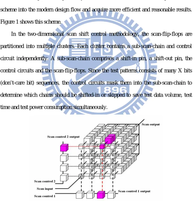
This chapter introduces the memory block concept for designing the multiple scan chain using two-dimensional scan-shift control architecture, which makes each sub-scan-chain operate independently in scan-in mode. Moreover, we implement this scheme into the modern design flow and acquire more efficient and reasonable results. Figure 1 shows this scheme.
In the two-dimensional scan shift control methodology, the scan-flip-flops are partitioned into multiple clusters. Each cluster contains a sub-scan-chain and control circuit independently. A sub-scan-chain comprises a shift-in pin, a shift-out pin, the control circuits and the scan-flip-flops. Since the test patterns consists of many X bits (don’t-care bit) sequences, the control circuits mask them into the sub-scan-chain to determine which chains should be shifted-in or skipped to save test data volume, test time and test power consumption simultaneously.
Figure 1. Proposed multiple scan chain architecture with 2-D 4x4 scan shift control chains. Combined with the proposed methodology, this test scheme achieves low test power, small data volume, and short test time.
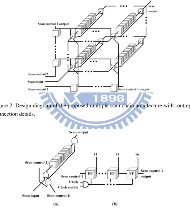
Figure 2 shows the design details of the multiple scan chain architecture. The scan control 1 applies control signals to the control circuit of each sub-scan-chain in each column. The scan control 2 provides the row base control signal. Figure 3 reveals the control circuit design logic gates. Scan control 1i in Figure 3 (a) connects to the scan-flip-flop signal 1i in Figure 3 (b). Scan control 2 uses the same idea to connect to the control signals. From Figure 2 and Figure 3, the scan input signals are masked if the control signal does not enable into the sub-scan-chain.
Figure 2. Design diagram of the proposed multiple scan chain architecture with routing connection details.
Figure 3. Circuit design of the proposed multiple scan chain architecture (a) is part of the sub-scan-chain design and (b) presents the details for one scan control chain.
This study applies two clustering approaches [17], [18] for a two-dimensional scan-shift control scheme and compares their performance including routing wire-length, test data volume and so on. As mentioned above, one cluster approach is the uniform cluster area for each cluster, and other is the uniform scan-flip-flop number in the clusters except one cluster. Once the cluster type is decided, the original scan-order is broken and then the scan-flip-flops are reordered into clusters to form each sub-scan-chain.
Chapter 3
Clustering and Reordering Method
This chapter introduces the clustering and routing methodology. The methodology consists of cluster approaches, locating the scan-flip-flops and reordering these sub-scan-chains. First, this study applies two clustering approaches to form the new scan-chain structure, resulting in different test time, test data volume, test power consumption and so on. Second, the scan-flip-flops will be located in each cluster without modifying the scan-flip-flop location to maintain functional timing. Finally, the sub-scan-chains are built and the reordering the sub-scan-chains keep the routing wire-length short.
3.1
Uniform cluster area approach
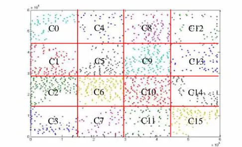
The chip partitions make each cluster area a uniform distribution. In other words, each cluster area is identical. Since the scan-flip-flops are randomly spread on a chip, the number of scan-flip-flops is not the same in each cluster. These scan-flip-flops form a sub-scan-chain with control circuits. Extreme case may not contain any scan flop-flop inside the cluster. Figure 4 shows an example of the ISCAS’99 benchmark circuit b17 with 4 scan flip-flops in the control circuits of scan-control-1 and scan-control-2, respectively.
Figure 4. Uniform cluster area approach. The area is identical, but the scan-flip-flop numbers are not equal in each cluster.
The chip is clustered. Subsequently, the original scan order should be broken and the scan-chain reordered within each cluster to form the sub-scan-chain. Furthermore, the test patterns are encoded and shifted into each sub-scan-chain from the scan-in pin. This work places both the scan-in pin and the control circuits near the center of each cluster. We can predict the routing length of the control circuits using uniform cluster area approach, since the scan-in pins and the control circuits are placed in regular locations.
3.2
Uniform scan-cell number approach
The scan-flip-flops in this approach are randomly distributed on a chip. This clustering approach depends on the number of scan-flip-flops to locate the cluster region and make the number of the scan-flip-flops equal in each cluster. The number of scan-flip-flops in clusters is as follows:
number number Cluster SC x= % (1) number number number SC x Cluster CELL =( − )/ (2) C0 C1 C2 C3 C4 C5 C6 C7 C8 C9 C10 C11 C12 C13 C14 C15
In this clustering approach, the scan-flip-flops number in each cluster is different. The number of scan-flip-flops in clusters is as follows:
number number
number
numberLast SC Cluster CELL
CELL = −( −1)* (3)
Practically, the test pattern length for each sub-scan-chain during encoding procedure in a two-dimensional scan-shift control scheme does not need to be recorded [21]. This encoding approach is more efficient and compact.
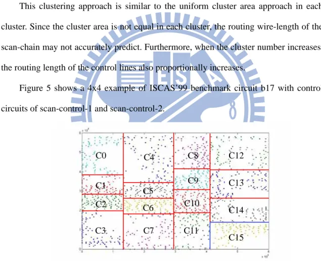
This clustering approach is similar to the uniform cluster area approach in each cluster. Since the cluster area is not equal in each cluster, the routing wire-length of the scan-chain may not accurately predict. Furthermore, when the cluster number increases, the routing length of the control lines also proportionally increases.
Figure 5 shows a 4x4 example of ISCAS’99 benchmark circuit b17 with control circuits of scan-control-1 and scan-control-2.
Figure 5. Uniform scan-cell number approach, the scan-flip-flop number is identical in all clusters except cluster C15. Since the test data contains many X-bits (don’t-care bits) and its pattern length does not need to be recorded during encoding, it contributes to more efficient and compact test patterns.
C0 C1 C2 C3 C4 C5 C6 C7 C8 C9 C10 C11 C12 C13 C14 C15
3.3
Locating the scan-flip-flop in each cluster
This work applies two clustering approaches without modifying the original placement of the scan-flip-flops to maintain functional timing. Since the original scan-order does not reference real placement of the scan-flip-flop, we break the scan-chain to form new sub-scan-chains in each cluster. Therefore the scan-flip-flops evaluate chip placement exactly and one scan-flip-flop is only located in one cluster either in the uniform cluster area approach or in the uniform scan-flip-flop number approach. The pseudocode for locating the scan-flip-flop procedure in the uniform cluster area approach shows below.
SC={SC1, SC2,...,SCn}; //Load the location for each scan cell
△X = Xmax / X_CLUSTER_No; //The cluster size in x-axis
△Y = Ymax / Y_CLUSTER_No; //The cluster size in y-axis
/* Locating the scan cell in every cluster */
for (SC){ //evaluation whole scan-cells for (X_CLUSTER_No){
for (Y_CLUSTER_No){ x++;
if (SCi_x-axis <= △X * X_CLUSTER_No && SCi_y-axis <= △
Y * Y_CLUSTER_No){
CLUSTERx = SCi; // SCi is located in CLUSTERx CELL_No ++; //The number of scan cells in the cluster } } } }
To begin, the clusters should indicate their coordinates and then the scan flop-flops in each cluster can be located.
Since the uniform scan-cell number approach locating the scan-flip-flops is different than the uniform cluster area approach, the current study develops another approach to locate the scan-flip-flops. The pseudocode for locating the scan-flip-flops
procedure in the uniform scan-cell number approach is as follows:
SC={SC1, SC2,...,SCn}; //Load the location for each scan cell
/* Locate the scan cells in each cluster */
for (SC){ //evaluation whole scan-cells
if(CLUSTER_No<=X_CLUSTER_No+Y_CLUSTER_No–1) //for last cluster
for (CLUSTER_CELL_No){
if (SCi_x-axis >= Xi−1&& SCi_x-axis <=X && SCi_y-axis >= i Yi−1
&& SCi_y-axis <= Y ){ i
CLUSTERx = SCi; // SCi is located in CLUSTERx}}} else{
CLUTERlast = SC - SCi;
3.4 Reordering
The scan-flip-flops are located in each cluster. The sub-scan-chain can form the decided scan-order. For scan-order, this work uses an identical heuristic to reorder the scan-flip-flops for both clustering approaches.
We first break the original scan order to form new sub-scan-chains in each cluster. The current approach shifts the test patterns into the sub-scan-chain from each shift-in pin where they are located near the cluster center. Depending on the placement, this investigation searches out the first order of the scan-flip-flop nearest the shift-in pin in each cluster. The first order of the scan-flip-flop dedicates in clusters to determine the next connected scan-flip-flop by the shortest Manhattan distance. According this procedure the scan-flip-flops travel inside a cluster and the sub-scan-chains form a new order. Once the sub-scan-chain ordering is formed in one of clusters, the same procedures apply to form the sub-scan-chain in other clusters. The following addresses the reordering procedure for the uniform cluster area approach:
for (CELL_NO_i){
if (Min (abs (SCi_x-axis – Shift-in_Location_x-axis)) + (abs (SCi_y-axis – Shift-in_Location_y-axis))){
SCi is connected to sub-shift-in; } //The first scan-flip-flop in the chain
then (Min (abs (SCi_x-axis – SCi+n_x-axis )) + (abs (SCi_y-axis –
SCi+n_y-axis ))){
SCi is connected to SCi+n; } }
The procedure for the uniform scan-cell number approach is presented as follows:
if(NOT_THE_LAST_CLUSTER){ for (CLUSTER_CELL_NO){
if (Min (abs (SCi_x-axis – Shift-in_Location_x-axis)) + (abs (SCi_y-axis – Shift-in_Location_y-axis))){
SCi is connected to sub-shift-in;}
then (Min (abs (SCi_x-axis – SCi+n_x-axis )) + (abs (SCi_y-axis –
SCi+n_y-axis ))){
SCi connected to SCi+n;} }
else(THE_LAST_CLUSTER){
for (CLUSTER_CELL_NO + x){ //for the last cluster if (Min (abs (SCi_x-axis – Shift-in_Location_x-axis)) + (abs (SCi_y-axis – Shift-in_Location_y-axis))){
SCi is connected to sub-shift-in;}
then (Min (abs (SCi_x-axis – SCi+n_x-axis )) + (abs (SCi_y-axis –
SCi+n_y-axis ))){
SCi is connected to SCi+n;} }
3.5
Implementing the modern design flow
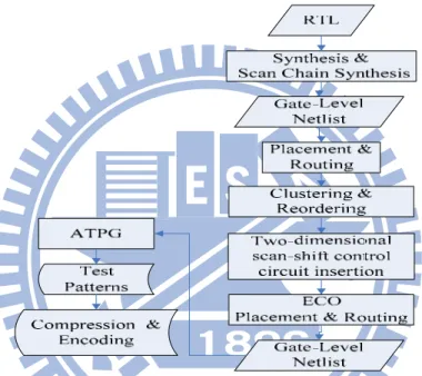
To realize the proposed testing scheme of modern design flow, we add an extra step to the design flow. Due to extra circuits, this work places the shift-in pin and control circuit in two-dimensional scan shift control methodology near the center of each cluster. These circuits are connected to the sub-scan-chains and inserted by the
ECO (Engineering Change Order) placement-and-routing procedure. Figure 6 shows the proposed modern design flow. Once the ECO placement-and-routing procedure is finished, the two-dimensional scan-shift control design integrates into the design completely thereby generating the new placement-and-routing result. The netlist through the ATPG (Automatic Test Pattern Generator) tools generates the test patterns. Moreover, the test patterns also use the efficient compression and encoding approach to reduce test data volume, test time and test power consumption [7], [8], [9] and [10].
Figure 6. Proposed modern design flow. To integrate the proposed testing scheme into the design flow, we insert the two-dimensional scan-shift control circuits and shift-in pins into the design flow. Once ECO placement-and-routing procedure is finished, the gate-level netlist is generated. The netlist through the ATPG tools generates the test patterns to evaluate the whole design.
Chapter 4
Experimental Results
The experimental results use the ISCAS’89 and ISCAS’99 benchmark circuits. The test patterns are generated by Synopsys TetraMax [19]. The placement-and-routing are generated by Synopsys Astro [20] and the technology is UMC’s 0.18um process. The interconnect length of scan chains is calculated by Manhattan distance between scan cells.
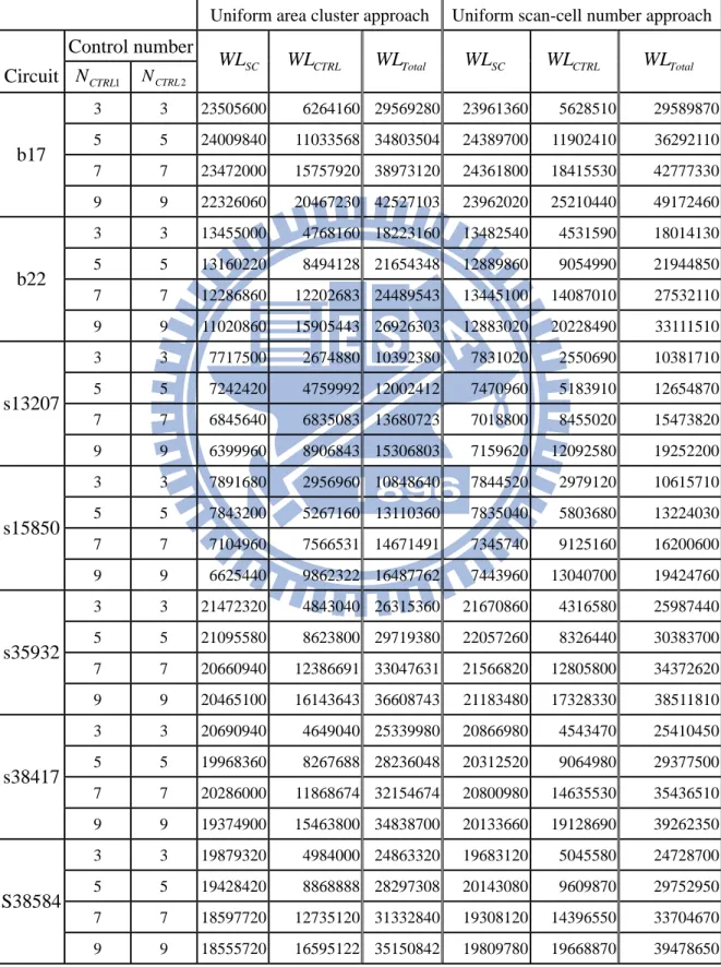
Table 1 shows the benchmark circuit characteristics. The second and third columns are the input pin and output pin of the circuit, respectively. The fourth column of the table shows the number of D-flip-flops. The fifth and sixth columns show the inverters and other combinational logic gates, respectively.
Table 1. Circuit characteristics of ISCAS’89 and ISCAS’99 benchmark, showing the DFF, inverters and combinational gates, input pin and output pin number.
Circuit Name #Input #Output #DFFs #INVs #Gates
b17 37 97 1415 4474 27852 b22 32 22 537 4491 25460 s13207 62 152 638 5378 2573 s15850 77 150 534 6324 3448 s35932 35 320 1728 3861 12204 s38417 28 106 1636 13470 8709 s38584 38 304 1426 7805 11448
Since the original benchmark circuits use the general D-flip-flop, these circuits are re-synthesized and replaced by D-flip-flops with scan-flip-flips by a Synopsys Design Compiler [22]. This study also uses the Synopsys’s Astro placement-and-routing tool
[20] to implement the physical design. The setting of the aspect ratio is 1 and the routing utilization is about 90%. Although the commercial tools implement a scan-chain or multi-scan-chain, these scan-chain styles do not meet the proposed scheme. Therefore, in this scheme, the commercial tool performs placement-and-routing to meet the timing for normal function and the scan-chain routing for reordering. The proposed scheme applies the two-dimensional scan control concept for multiple scan-chain design to shift the test patterns into each sub-scan-chain and then evaluate the whole chip. Table II shows the experiment results on ISCAS’89 and ISCAS’99 benchmark circuits and presents the routing length for different clusters on benchmark circuits in two approaches, one for the uniform cluster area approach, and other for the uniform scan-flip-flop number approach. The second and third columns are the number of control circuits scan-control-1(NCTRL1) and scan-control-2 (NCTRL2), respectively. The
SC
WL is the total wire-length of the sub-scan-chains. The WLCTRL is the total
wire-length of the control lines, including scan-control-1, scan-control-2, shift-in and shift-out. The WLTotal is the total wire-length and the sum of WL and SC WLCTRL.
This experiment results chapter has two phases, the evaluation phase, and the physical placement-and-routing phase. In the evaluation phase, we use the C program to quickly and roughly evaluate the results for wire-length in both clustering approaches. The result in this phase is only for evaluation. In the physical placement-and-routing phase, the routing will depend on the reordering result, which will input into the proposed modern design flow to realize the scheme. We use the Synopsys Astro to implement placement-and-routing. The technology process is UMC 0.18µm, the metal layer is 1P5M.
of the scan chain without including normal function routing. The WLTotal in the
uniform scan-cell number approach is longer than that in the uniform cluster area approach, especially when the cluster number increases. When the cluster number is small, the total wire-length of the sub-scan-chain also reduces in the uniform cluster area approach.
Moreover, the total wire-length of the sub-scan-chain is almost identical in the different cluster sizes for the uniform scan-cell number approach. In this approach, each cluster area is different, and the routing length of control lines is not regular. Since the Manhattan distance calculates wire-length, the routing-length may be longer. The control lines also crossover a chip, hence they dominate the total wire-length in larger cluster number especially using the uniform scan-cell number approach. For example, when the control lines number NCTRL1 and NCTRL2 are both 9, respectively, the total wire-length of the uniform scan-cell number approach is longer than the total wire-length of the uniform cluster area approach of about 15.6%.
Although the total wire-length is longer in the uniform scan-cell number approach, the test data encoding may be more efficient than the uniform cluster area approach based on the two-dimensional scan-shift control scheme. The two-dimensional scan-shift control scheme provides the test patterns encoding for the uniform scan-cell number approach, but it is not for the uniform cluster area approach [21]. Therefore, compared with power consumption, test data volume and test time, we find the proper trade-off in either the uniform scan-cell number approach or the uniform cluster area approach.
Table 2. Wire-length results of ISCAS’89 and ISCAS’99 benchmark circuits by applying different numbers of clusters and implementing both approaches, the uniform cluster area approach, and the uniform scan-cell number approach. The WLTotal is the sum of WL and SC WLCTRL compared with the wire-length in both approaches.
Uniform area cluster approach Uniform scan-cell number approach Control number Circuit NCTRL1 NCTRL2 SC WL WLCTRL WLTotal WLSC WLCTRL WLTotal 3 3 23505600 6264160 29569280 23961360 5628510 29589870 5 5 24009840 11033568 34803504 24389700 11902410 36292110 7 7 23472000 15757920 38973120 24361800 18415530 42777330 b17 9 9 22326060 20467230 42527103 23962020 25210440 49172460 3 3 13455000 4768160 18223160 13482540 4531590 18014130 5 5 13160220 8494128 21654348 12889860 9054990 21944850 7 7 12286860 12202683 24489543 13445100 14087010 27532110 b22 9 9 11020860 15905443 26926303 12883020 20228490 33111510 3 3 7717500 2674880 10392380 7831020 2550690 10381710 5 5 7242420 4759992 12002412 7470960 5183910 12654870 7 7 6845640 6835083 13680723 7018800 8455020 15473820 s13207 9 9 6399960 8906843 15306803 7159620 12092580 19252200 3 3 7891680 2956960 10848640 7844520 2979120 10615710 5 5 7843200 5267160 13110360 7835040 5803680 13224030 7 7 7104960 7566531 14671491 7345740 9125160 16200600 s15850 9 9 6625440 9862322 16487762 7443960 13040700 19424760 3 3 21472320 4843040 26315360 21670860 4316580 25987440 5 5 21095580 8623800 29719380 22057260 8326440 30383700 7 7 20660940 12386691 33047631 21566820 12805800 34372620 s35932 9 9 20465100 16143643 36608743 21183480 17328330 38511810 3 3 20690940 4649040 25339980 20866980 4543470 25410450 5 5 19968360 8267688 28236048 20312520 9064980 29377500 7 7 20286000 11868674 32154674 20800980 14635530 35436510 s38417 9 9 19374900 15463800 34838700 20133660 19128690 39262350 3 3 19879320 4984000 24863320 19683120 5045580 24728700 5 5 19428420 8868888 28297308 20143080 9609870 29752950 7 7 18597720 12735120 31332840 19308120 14396550 33704670 S38584 9 9 18555720 16595122 35150842 19809780 19668870 39478650
Figure 7 (a) and (b) demonstrate the distribution of the wire-length in the two-dimensional scan shift control structure for different types of scan-control lines on ISCAS’99 benchmark circuit b17. The number of scan-line-1 lines and scan-control-2 lines are from 3 to 15, respectively. (a) shows results of the uniform scan-cell number approach and (b) shows results of the uniform cluster area approach. Both of them represent that when scan-control lines increase, total routing wire-length also increases. Therefore, the figures show the trade-off between routing length, test power consumption, test data volume and test time [21].
0.E+00 1.E+07 2.E+07 3.E+07 4.E+07 5.E+07 6.E+07 7.E+07 8.E+07 WL 3 7 11 15 3 7 11 15 Scan-Control-1 Scan-Control-2 b17 Total WL in Uniform Scan-Cell Number Approach
(a) 0.E+00 1.E+07 2.E+07 3.E+07 4.E+07 5.E+07 6.E+07 WL 3 7 11 15 3 7 11 15 Scan-Control-1 Scan-Control-2 b17 Total WL in Uniform Cluster Area Approach
(b)
Figure 7. (a) and (b) demonstrate the wire-length distribution in the two-dimensional scan shift control structure for different types of scan-control lines on ISCAS’99 benchmark circuit b17. The unit of the wire-length is µm.
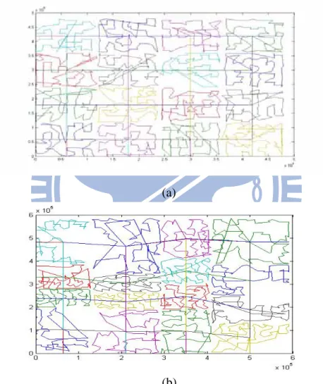
Since the Manhattan distance calculates wire-length, the wire-length of the control lines in the uniform cluster area approach is shorter than that in the uniform scan-cell number approach. The wire-length of the sub-scan-chain does not have large variation during different cluster sizes in both clustering approaches. Therefore, the wire-length of the control line dominates the total wire-length. Figure 8 shows the result of the sub-scan-chains order.
(a)
(b)
Figure 8. Reordering result of b17 circuit, the scan-control-1 and scan-control-2 are 4, respectively. (a) represents the uniform cluster area approach and (b) represents the uniform scan-cell number approach. The longer lines are the scan-control, shift-in and shift-out lines. These lines spread through the whole chip. The scan-control circuits are placed in the center of each cluster by default.
4.2 Physical
Placement-and-Routing
Phase
Table 3 shows the physical routing result, using the Synopsys Astro placement-and-routing tool [19] to route the original netlist and each circuit in different cluster numbers. This physical placement-and-routing result uses the UMC 0.18µm and 1P5M (1-poly and 5-metal layers) process.
Table 3. Physical routing result of the circuit b17 of ISCAS’99. The technology process is UMC 0.18µm and 1P5M. The WLTotal represents the total wire-length and the unit
is in µm. The CTotal is the total contact number and it also shows placement
utilization for each circuit. Each circuit area is identical and the area is 633µm*628µm.
Original Uniform Area Cluster Approach Uniform Scan-Cell Number Approach Cluster Number Cluster Number
Single scan-chain
3x3 5x5 7x7 3x3 5x5 7x7
Total
WL 950635 1064683 1066268 1085384 1068556 1073299 1126204 Utilization 89.31% 90.05% 91.37% 93.35% 90.05% 91.37% 93.35%
Comparing Table 2 and Table 3 routing length results, Table 2 results only use a single metal layer to evaluate the routing length and Table 3 results use physical routing tools to implement. The process is UMC 0.18µm and the metal layer is 1P5M. Because Table 3 uses multi-metal-layer for routing, it can dramatically shorten the routing length compared to that of single layer routing. In practice, modern VLSI routing is used for multi-metal-layer routing to guarantee routing implementation within a reasonable chip area.
In Table 3, Synopsys Astro [19] optimizes original netlist reordering, routing length and placement utilization as a single scan-chain design. The experiment results represent the routing length and placement utilization rate in cluster numbers of 3x3,
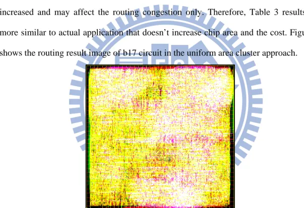
5x5 and 7x7 respectively for the uniform area cluster approach and the uniform scan-cell number approach. Comparing routing length, contact number and placement utilization for cluster numbers 7x7 in both clustering approaches to the original netlist, the routing length is longer 9.9% and 14.08%, the contact number is greater 4.78% and 5.4% and the placement utilization rate is greater 4.04% than that of clustering approaches and the original netlist respectively. Although clustering approaches may use more routing resources and add extra control circuits, the proposed approaches adjust the appropriate utilization rate within the routable region, the chip area is not increased and may affect the routing congestion only. Therefore, Table 3 results are more similar to actual application that doesn’t increase chip area and the cost. Figure 9 shows the routing result image of b17 circuit in the uniform area cluster approach.
Chapter 5
Conclusions
This thesis applies two clustering approaches [17] and [18] to partition scan cells and use the shortest Manhattan distance to reorder the scan cells. Finally, this work implements the two-dimensional scan shift control test scheme into the modern testing design flow. This scheme has many benefits that reduce test data volume, test time and test power consumption with small area overhead. The current study also compares the two clustering approaches in routing length. Findings show that the uniform cluster area approach is better than the uniform scan-cell number approach especially in large cluster size. Furthermore, in the chip area, we adjust the appropriate utilization rate within the routable region. The chip area is not increased and may effect routing congestion only.
This work obtains the most advantages during testing in this scheme. However, we should take care the routing length and the routing resource. The control lines distribution in the chip are regular, the routing may be treated as a clock-tree in placement-and-routing procedure without affecting the driving and skew of the normal function.
For uniform cluster area approach, we do not provide an encoding approach. For this reason, the test data volume and the test power consumption are not reduced. But this architecture still is as a multiple scan chain, the test time can be reduced that compared with the single scan chain architecture.
These experiment results provide a tradeoff between the two clustering approaches. Moreover, these clustering and routing approaches can further extend test structures such as three-dimension or other multiple-dimensional types.
For test pattern encoding, we should find the more efficient and lower overhead approaches such as average the scan cells in each cluster as possible to gain the encoding efficiency and benefits in test data volume, test time and test power consumption especially for uniform cluster area approach.
References
[1] P. Girard, “Survey of Low-Power Testing of VLSI Circuit,” in Proc. of IEEE Design & Test of Computers, Vol. 19, No. 3, pp. 80-90, 2002.
[2] A. Crouch. “Design-for-Test for Digital IC’s and Embedded Core Systems” Prentice Hall, 1999.
[3] C. P. Ravikumar, M. Hirech, and X. Wen, “Test Strategies for Low Power Devices,” in Proc. of Design, Automation, and Test in Europe, pp. 728-733, 2008. [4] K-J. Lee, J-J. Chen, and C-H. Huang, “Using a Single Input to Support Multiple
Scan Chains,” in Proc. of International Conference on Computer-Aided Design, pp. 74-78, 1998.
[5] M. Elm, H.-J. Wunderlich, M.E. Imhof, C.G. Zoellin, J. Leenstra, N. Maeding, “Scan Chain Clustering for Test Power Reduction,” in Proc. of ACM/IEEE Design Automation Conference, pp. 828-833, 2008.
[6] Il-soo Lee, Yong Min Hur, T. Ambler, “The Efficient Multiple Scan Chain Architecture Reducing Power Dissipation and Test Time,” in Proc. of Asian Test Symposium, pp. 94-97, 2004.
[7] A. Chandra and K. Chakrabarty. “Low-Power Scan Testing and Test Data Compression for System-on-a-Chip,” IEEE Transactions on Computer-Aided Design of Integrated Circuits and Systems, Vol. 21, No. 5, pp.597-604, May 2002. [8] M. Nourani, M. Tehranipour and K. Chakrabarty, “Nine-coded Compression
Technique with Application to Reduced Pin-count Testing and Flexible On-chip Decompression,” in Proc. of Design, Automation, and Test in Europe, Vol.2, pp. 1284-1289, Feb. 2004.
[9] H. Tang, S. M. Reddy and I. Pomeranz, “On Reducing Test Data Volume and Test Application Time for Multiple Scan Chain Designs,” in Proc. of IEEE International Test Conference, Vol. 1, pp. 1079-1088, 2003.
[10] C.-Y. Lin and H.-M. Chen, “A Selective Pattern-Compression Scheme for Power and Test-Data Reduction,” in Proc. of International Conference on Computer-Aided Design, pp. 520-525, 2007.
[11] J. Lee and Nur A. Touba, “LFSR-reseeding Scheme Achieving Lowpower Dissipation During Test,” IEEE Transactions on Computer-Aided Design of Integrated Circuits and Systems, Vol. 26, No.2, pp. 396-401, Feb. 2007.
[12] G. Mrugalski, J. Rajski, D. Czysz, and J. Tyszer, “New Test Data Decompressor for Low Power Applications,” in Proc. of ACM/IEEE Design Automation Conference, pp. 539-544, 2007.
[13] J. Rajski, J. Tyszer, M. Kassab, and N. Mukherjee, “Embedded deterministic test,” IEEE Transactions on Computer-Aided Design of Integrated Circuits and Systems, Vol. 23, No. 5, pp. 776-792, 2004.
[14] H. Ando, “Testing VLSI with Random Access Scan,” in Proc. of the COMPCON, pp. 50-52, Feb. 1980.
[15] D. H. Baik and K. K. Saluja, “Progress Random Access Scan: A simultaneous Solution to Test Power, Test Data Volume and Test Time,” in Proc. of IEEE International Test Conference, pp. 359-368, 2005.
[16] Y. Hu, X. Fu, X. Fan, H. Fujiwara, “Localized random access scan: towards low area and routing overhead,” in Proc. of Asia and South Pacific Design Automation Conference, pp. 565-570, March 2008.
[17] Y. Bonhomme, P. Girard, L. Guiller, C. Landrault, S. Pravossoudovitch, and A. Virazel. “Design of Routing-Constrained Low Power Scan Chains,” in Proc. of
[18] Y. Bonhomme, P. Girard. L. Guiller, C. Landrault, S. Pravossoudovitch, “Efficient Scan Chain Design for Power Minimization During Scan Testing Under Routing Constraint,” in IEEE International Test Conference, Vol.1, pp. 488–493, 2003. [19] TetraMax. Synopsys Inc.
[20] Astro. Synopsys Inc.
[21] C.-Y. Lin and H.-M. Chen, “A Novel Two-Dimensional Scan-Control Scheme for Test-Cost Reduction,” Proceedings of the 20th VLSI Design/CAD Symposium, Hualien, Taiwan, August 2009
![Table 3 shows the physical routing result, using the Synopsys Astro placement-and-routing tool [19] to route the original netlist and each circuit in different cluster numbers](https://thumb-ap.123doks.com/thumbv2/9libinfo/8146685.166926/28.892.176.803.390.786/physical-synopsys-placement-original-circuit-different-cluster-numbers.webp)