國
立
交
通
大
學
材料科學與工程研究所
博 士 論 文
以電漿輔助式分子束磊晶成長應用於高電子遷移率
電晶體之氮化鋁鎵/氮化鎵異質結構
Epitaxial Growth of AlGaN/GaN Heterostructure by Plasma-Assisted Molecular
Beam Epitaxy for High Electron Mobility Transistor Applications
研 究 生:黃延儀
指導教授:張 翼 教授
以電漿輔助式分子束磊晶成長應用於高電子遷移率
電晶體之氮化鋁鎵/氮化鎵異質結構
Epitaxial Growth of AlGaN/GaN Heterostructure by Plasma-Assisted Molecular
Beam Epitaxy for High Electron Mobility Transistor Applications
研 究 生:黃延儀 Student:Yuen-Yee Wong
指導教授:張 翼 Advisor:Edward Yi Chang
國 立 交 通 大 學
材料科學與工程研究所
博 士 論 文
A Thesis Submitted to Department of Materials Science and Engineering
National Chiao Tung University
in partial Fulfillment of the Requirements
for the Degree of Doctor of Philosophy in
Materials Science and Engineering
July 2011
Hsinchu, Taiwan, Republic of China
i
以電漿輔助式分子束磊晶成長應用於高電子遷移率電晶體之氮化鋁鎵/氮
化鎵異質結構
學生:黃延儀
指導教授:張 翼 博士
國立交通大學材料科學與工程研究所
摘要
本論文利用電漿輔助式分子束磊晶在藍寶石基板上成長應用於高電子遷移率電晶 體元件製作之氮化鋁鎵/氮化鎵異質結構。我們首先探討氮化鋁緩衝層成長條件對氮化 鎵薄膜缺陷結構的影響。在較低溫度成長的氮化鋁緩衝層上,由於表面比較粗糙,氮化 鎵薄膜裏的刃線差排密度會降低,但螺旋線差排密度會增加。這是因爲粗糙的氮化鋁表 面有助於彎曲刃線差排的成長方向,促進刃差排的交互作並減低其密度。另一方面,粗 糙的氮化鋁表面因爲有許多讓螺旋差排形成的成核點,導致螺旋差排的密度增加。進一 步的試驗也發現刃線差排與氮化鋁緩衝層的厚度息息相關。大或小於最佳的厚度(15 奈米),都會造成氮化鎵薄膜的應力上升並增加刃線差排的密度。 爲了有效的降低差排密度,我們利用了在鎵貧乏成長條件下成長的氮化鎵緩衝層。 鎵貧乏的氮化鎵緩衝層表面有許多小平臺及溝槽,溝槽裏的斜壁提供了很好的方法以彎 曲刃差排的成長方向並促進差排得交互作用。通過提升差排的互相結合及消滅效應,鎵 貧乏緩衝層能更有效的降低刃差排的密度。另,鎵貧乏緩衝層也能有效的抑制螺旋差排 的產生。因此把鎵貧乏的氮化鎵緩衝層成長在平滑表面的氮化鋁緩衝層(可利用高溫成 長)上,就能有效的減少氮化鎵薄膜裏的所有差排密度。爲了修復粗糙的氮化鎵緩衝層 表面,我們也開發了氮化鎵的遷 移 促 進 磊 晶 技術。這方法是由交替沉積鎵和氮原子於 試片表面上來完成。結合鎵貧乏的氮化鎵緩衝層及遷 移 促 進 磊 晶 技 術,我 們 利 用 分 子束磊晶成長出低差排密度(~2x108 cm-2 ) 以 及 擁 有 平 滑 表 面 的 氮化鎵薄膜。 最後,我們也研究了不同差排缺陷對氮化鋁鎵/氮化鎵異質結構的電性特性影響。ii 從霍爾量測中發現,其異質界面通道裏的二維電子遷移率主要受限於刃差排的密度。這 是因爲刃差排缺陷趨向於捕捉電子,形成庫倫散射中心並減緩通道裏的電子遷移率和增 加通道的阻值,所以刃差排將降低電子元件的電流密度和操作頻率。另一方面,從蕭基 二極體的量測可得知,螺旋差排像有如讓縱向電流流通的路徑,非常不利於閘極的逆向 偏壓漏電流,導致元件的崩潰電壓變差。因此,要製作高品質的高電子遷移率電晶體元 件,氮化鋁鎵/氮化鎵材料裏的各種差排密度必須降低。
iii
Epitaxial Growth of AlGaN/GaN Heterostructure by Plasma-assisted Molecular
Beam Epitaxy for High Electron Mobility Transistor Applications
Student: Yuen-Yee Wong Advisor: Dr. Edward Yi Chang Department of Materials Science and Engineering
National Chiao Tung University
Abstract
AlGaN/GaN heterostructure for the high electron mobility transistor applications were grown by plasma-assisted molecular beam epitaxy (PA-MBE) on the sapphire substrates. The effects of AlN buffer growth parameters on the defect structure on GaN film were first investigated. For GaN film grown on lower-temperature buffer, the density of screw threading dislocation (TD) was increased while the density of edge TD was decreased. The rough AlN surface helped to bend the growth direction of edge TDs and then reduced the dislocation density through recombination and annihilation processes. However, the screw TD was increased on the rough AlN buffer because this surface provided many nucleation centers for screw dislocation. Further examinations revealed that the edge TD was also closely related to the AlN buffer thickness which corresponding to the stress in GaN film. Total TD density could be minimized by optimizing the AlN buffer growth temperature and thickness.
GaN buffer grown at Ga-lean condition was found useful to reduce the edge TD density in the GaN film significantly. The Ga-lean buffer, with inclined trench walls on its surface, provides an effectively way to bend the propagation direction and promotes the interaction of edge TDs in the GaN film. As a result, the edge TD density was reduced by approximately two orders of magnitude to 2x108 cm-2. The rough surface of Ga-lean buffer was recovered using migration enhanced epitaxy (MEE), a process of alternating deposition cycle of Ga atoms and N2 radicals, during the PA-MBE growth. By growing the Ga-lean GaN buffer on a
iv
smooth AlN buffer (achieved by high temperature), both the edge and screw TDs in the GaN film could be effectively reduced.
Finally, the roles played by different types of TDs on the electrical properties of AlGaN/GaN heterostructure were studied. From the Hall measurement, the electron mobility in two-dimensional electron gas channel was mainly controlled by the edge TDs. The edge TD acted as Coulomb scattering centers inside the channel and reduced the carrier mobility and increased its resistance. On the other hand, from the Schottky barrier diode characterization, the screw TDs which acted at the current leakage path and was more deleterious to the gate reverse-bias leakage current of the AlGaN/GaN structure. As a result, the output current density and operating frequency of the HEMT devices were decreased by the edge TDs while the device breakdown voltage was degraded by the screw TDs. Therefore, for high performance HEMT device fabrication, both screw and edge TD densities in the AlGaN/GaN material have to be minimized.
v
Acknowledgement
誌謝
2006 年初,有機會來到了張翼老師的實驗室(CSDLab),展開了我在交通大學的博士 生學習與研究生涯。幾年下來,非常感激張翼老師的教導以及所給于的各種機會。另外, 實驗室及學校完善的半導體設備與交大材料所老師們提供的基礎教學訓練,讓我得以從 頭學起半導體的相關材料與元件,真的受益非淺。 在來到交大的初期,很幸運的可以加入由楊宗熺學長領導的 MBE 長晶小組工作,讓 我結交到一群非常要好的夥伴。除了宗熺學長還有哲榮,瑞泰,怡誠和詩國,我很懷念 大夥兒一起學習,一起討論,一起去玩的日子,也感謝你們在日常生活上給于的各種協 助,讓我在臺灣的生活倍感窩心。在利用 MBE 長晶的歲月裏,還要感謝 ULVAC 公司及員 工,特別是陳江耀,陳建瑩,張晃崇學長等對機台的維修及保養所付出的努力,還有在 試驗上的幫忙及支持。此外還要感激凃搏閔經常提供 GaN template 給我做實驗,多次 的 Hall 量測及長晶方面的意見。 特別感謝 CSDLab 製程組的瑞乾,宗育,家達與昱盛在元件製作上的幫忙和電性量 測上的協助。當然還有其他資深的學長如岳欽,建億,雲驥,你們的指導讓我對元件物 理有了更深入的了解。還要謝謝龔梁,佑霖,偉進,Tung,Tinh 和電物所的振豪提供在 長晶方面的協助。吳岳翰學長在 TEM 方面的專業協助也確實讓我增長了學多寶貴知識。 最重要的是要感謝我最摯愛的父母及家人,你們的包容與支持一直是我往前邁進的 動力,也讓我有非常大的自由發展空間,可以盡情的做自己感興趣的事,過快樂滿足的 人生。 在博士班的學習過程中曾經受過無數的恩惠,除了老師,學長,同學,朋友,還有 學校的行政人員,認識或不認識的人士,也感謝你們。請原諒我沒能一一提及,除了感 激,也祝福你們,願各位身體健康,萬事順利。vi
Contents
Abstract (Chinese) ………... i
Abstract (English) ……… iii
Acknowledgement ………... v Contents ………... vi Table Captions ……..……… ix Figure Captions …..….……….. x
Chapter 1
Introduction
1.1 Background ………... 1 1.2 AlGaN/GaN HEMTs ………. 21.3 Material growth of GaN ……… 3
1.4 Growth of GaN by MBE on sapphire ………... 5
1.4.1 AlN buffer layer ……… 5
1.4.2 Growth temperature ……….. 6
1.4.3 III-V ratio ……….. 6
1.5 Objective of the study and organization of this thesis ……….. 7
Tables ………... 9
Figures ……….. 11
Chapter 2 Plasma-Assisted Molecular Beam Epitaxy System, Experimental
Procedure and Characterization Methods
2.1 Plasma-Assisted MBE system ……… 122.1.1 Chamber and vacuum pumps ………. 12
2.1.2 Sample manipulator and growth sources ………... 13
2.1.3 Analytical instruments and others ……….. 13
2.2 Growth Procedures ………. 14
2.2.1 Sample preparation ………. 14
2.2.2 Nitridation ………15
2.2.3 Growth of buffer layer ……….16
2.2.4 Growth of GaN layer ……….. 16
2.3 Characterization Measurements………... 17
2.3.1 Field emission scanning electron microscope (FE-SEM) ………... 18
2.3.2 Atomic force microscope (AFM) ……… 18
2.3.3 High resolution X-ray diffraction (HRXRD) ……….. 19
2.3.3.1 Rocking curves (-scan) ………. 19
vii
2.3.3.3 X-ray reflectivity (XRR) scan ………... 22
2.3.3.4 Reciprocal space mapping (RSM) ………... 22
2.3.3.5 Triple axis diffraction ……….. 23
2.3.4 Transmission electron microscope (TEM) ……….. 23
2.3.5 Hall effect measurement ………. 24
2.3.6 Capacitance-voltage (CV) and current-voltage (IV) measurement ………… 25
2.3.7 Direct electrical current (DC) measurement ………... 26
Tables ……… 27
Figures ………... 28
Chapter 3 Effect of AlN Buffer Growth Parameters on the Defect Structure of
GaN Grown by Plasma-assisted Molecular Beam Epitaxy
3.1 Introduction ……… 303.2 Experiment procedures ………... 30
3.3 Results and discussion ……… 31
3.3.1 Influence of growth temperature ……… 31
3.3.1.1 Correlation between defect structure and residual stress ……….... 32
3.3.2 Influence of AlN thickness ……….. 36
3.4 Conclusions ………. 39
Tables ………... 40
Figures ……….. 41
Chapter 4 Dislocation Reduction in GaN film Using Ga-lean GaN buffer
Layer and Migration Enhanced Epitaxy
4.1 Introduction ………. 464.2 Experimental procedures ………. 47
4.3 Results and discussion ……… 49
4.3.1 Recovering of rough GaN surface by MEE ………. 49
4.3.2 Reduction of dislocation density by Ga-lean GaN buffer ……… 51
4.4 Conclusions ………. 56
Figures ………... 57
Chapter 5 The Roles of Threading Dislocation on the Electrical Properties of
AlGaN/GaN Heterostructure Grown by MBE
5.1 Introduction ……… 625.2 Experiment procedures ……….. 63
5.3 Results and discussion ……….... 65
viii
5.3.2 Effects of TD on the electron mobility ………... 65
5.3.3 Effects of TD on the reverse-bias leakage current ……….. 67
5.4 Conclusions ………. 69 Tables ………... 71 Figures ……….. 72
Chapter 6
Conclusions
………. 75References
……… 77Vita
………. 83Publication List
………... 84ix
Table Captions
Table 1.1 Advantages of GaN material for electronic applications ………. 9 Table 1.2 Material properties of GaN, AlN, Si, SiC and sapphire ………9 Table 1.3 Comparison of 2DEG mobility and sheet carrier concentration of AlGaN/GaN
structure grown by MOCVD and MBE on different substrates ………. 10 Table 2.1 The optimized growth parameters of GaN using ULVAC MBE system …………. 27 Table 3.1 FWHM of GaN (0002) and (10-12) planes grown on different AlN buffer growth
temperatures ……… 40 Table 5.1 FWHM of GaN (0002) and (10-12) planes prepared on buffers with different
x
Figure Captions
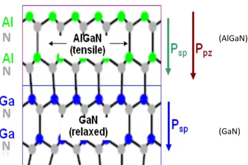
Fig. 1.1 (a) Polarization effect on the AlGaN/GaN structure. Psp and Ppz are spontaneous and
piezoelectric polarizations, respectively. (b) Carriers at the 2DEG are induced by the surface traps (charges) and polarization field in the AlGaN/GaN structure ………. 11 Fig. 2.1 Schematic diagram of the PA-MBE system ………... 28 Fig. 2.2 RHEED pattern of sapphire substrate (a) before nitridation, (b) after 30min nitridation and (c) after 60min nitridation ……….. 28 Fig. 2.3 RHEED pattern of the surface of (a) AlN, (b) GaN during growth and (c) GaN after
cooling to <200oC ………. 29 Fig. 2.4 Schematic diagram of the BEDE D1 HRXRD system ……….. 29 Fig. 3.1 Typical RHEED patterns for (a) AlN buffer layer, (b) GaN film during growth and (c) GaN film after cooling ……….. 41 Fig. 3.2 The screw and edge TDs densities of GaN grown on AlN buffer layers with different
growth temperatures ……….. 42 Fig. 3.3 The dependence of edge TD density on the elongation of c-axis lattice constant for the GaN grown on grown on AlN buffer layers prepared at different temperatures. 42 Fig. 3.4 AFM images of AlN buffers grown at temperature (a) 450 oC, (b) 740 oC and (c) 840
o
C ………... 43 Fig. 3.5 SEM images of GaN surfaces grown on AlN buffer prepared at (a) 525 oC, (b) 485 oC and (c) 450 oC ………... 44 Fig. 3.6 The dependence of the XRD (10-12) FWHM and elongation of c-axis lattice constant
on AlN buffer thickness ……… 45 Fig. 4.1 RHEED patterns of (a) smooth GaN surface and (b) rough Ga-lean GaN buffer
surface ……….. 57 Fig. 4.2 AFM images of the Ga-lean GaN surface after (a) 0, (b) 300, (c) 600 and (d) 800
xi
Fig. 4.3 The proposed mechanism of MEE to recover the rough GaN surface grown under Ga-lean condition ………. 58 Fig. 4.4 (a) Asymmetric (10-12) rocking curves of the GaN film at different stages of growth.
Inset shows the FWHMs of GaN symmetric (0002) deflection peaks after different MEE cycles. (b) Estimation of dislocation densities in GaN samples from the XRD results. The ‘2.5m’ represents the XRD results for the Sample A with 2.5m GaN film .……….. 59 Fig. 4.5 Cross-sectional TEM images of GaN grown (a) with and (b) without Ga-lean GaN
buffer layer ……… 60 Fig. 4.6 (a) Cross-sectional TEM image of GaN film near the Ga-lean buffer region. The dashed line shows the top of the Ga-lean buffer layer. Arrows indicate the locations of vertical TDs (VTD) and bent TDs (BTD). (b) Cross-sectional profile obtained from the AFM image in Fig. 4.2 (a). Some of the slopes on the profile are indicated ……… 61 Fig. 5.1 AFM images of the typical as-grown (a) GaN and (b) AlGaN surfaces. Inserts show their corresponding RHEED patterns ………... 72 Fig. 5.2 Hall electron mobility of AlGaN/GaN samples as a function of edge TD density.
Insert shows the effect of screw TD density on electron mobility. Open symbols in the diagrams represent the values for sample D ………... 73 Fig. 5.3 Sheet resistance and carrier concentration of the AlGaN/GaN samples as a function of
edge TD density. Open symbols represent the values for sample D ………. 73 Fig. 5.4 The reverse bias currents of AlGaN/GaN Schottky barrier diode samples. Insert shows the reverse bias current for sample A, B and C at -5V as a function of screw TD density ………. 74 Fig. 5.5 The reverse bias currents of AlGaN/GaN Schottky barrier diode samples as a function of sheet carrier density in the 2DEG ………. 74
1
Chapter 1
Introduction
1.1 BackgroundGaN is an interesting material because of its unique properties for both electrical and optical devices. With its wide direct bandgap and high electron mobility characteristics, GaN is an idea semiconductor material for the high power and high frequency electronics applications. Besides, GaN is also a physically hard material that makes it easier to handle during the fabrication. What has attracted earlier attention on this material is the fact that it can generate blue color light if made into the solid-state lighting devices, such as LEDs and laser diodes, completing the range of primary colors for lighting purposes. Despite the extraordinary properties of GaN material, to achieve device quality GaN is not easy. In contrast to the Si or GaAs materials, large-size native substrate for the growth of GaN materials is not available. This is the main obstacle which has hindered the progress of the GaN devices in the 1980s‟. Fast development of GaN devices began following the successful attempt to grow high quality GaN crystal on sapphire for LED devices by Shuji Nakamura in the beginning of 90s‟ [1]. Apart from the optical devices, the remarkable properties of the GaN materials are also found its niche electronic applications. The high energy bandgap and high electron saturation velocity of GaN have made it the superior material for high-speed and high-power electronics applications, especially for the wireless communication equipment.
2
Table 1.1 describes some of the benefits of using GaN for electronic applications. In this thesis, the high quality GaN materials for the fabrication of electronic devices, especially the high electron mobility transistor, were grown using molecular beam epitaxy (MBE) on sapphire substrates.
1.2 AlGaN/GaN HEMTs
As described above, GaN high electron mobility transistors (HEMTs) are excellent candidates for high power and high frequency applications. GaN materials for HEMT fabrication consists of a higher bandgap material, such as AlGaN [2] or AlInN [3], growth on top of the GaN film as the barrier layer. The discontinuity in conduction bands between the two materials forms a 2-diamentional electron gas (2DEG) channel at the hetero-interface. The 2DEG enables better electron confinement and less carrier scattering. Therefore, high electron mobility (~2000 cm2/V-s) can be achieved on an AlGaN/GaN heterostructure. AlGaN/GaN HEMT does not require intentional doping in the barrier or buffer layer to provide carrier in the 2DEG channel. Carriers in the 2DEG of GaN HEMT are originated from the material surface states and driven into the channel by the polarization field in the material (Fig. 1.1) [2]. Due to the strong polarization effect and large amount of surface states, high electron density (~1.5x1013 cm-2) can be induced at the 2DEG by AlGaN barrier layer with Al~25%. As a result of both high mobility and high carrier density, AlGaN/GaN HEMT
3
device of high current density (>2 A/mm) has been demonstrated [4].
1.3 Material growth of GaN
Due to the lack of large-size and low-cost commercial-grade native substrate, GaN materials are usually grown on the foreign substrates such as sapphire, silicon or silicon carbide. Table 1.2 shows some of the material properties of these substrates as compared to the GaN and AlN layers. Generally, the lattice constants and thermal expansion coefficients of these substrates differ significantly (except SiC) from that of GaN. As a result of these mismatches, large amount of dislocations are generated in the GaN film. The quality of the GaN film is therefore critically dependent on the ability of the transition layer (buffer layer) used to accommodate the stress generated from these mismatches. The commonly used buffer layers include low temperature GaN [1, 5], AlN [6-8] or their variations [9-11]. Dislocations generated in GaN are mainly screw, edge and mixed TDs. Besides the buffer layers, other approaches are also used occasionally to further improve the crystal quality of GaN film such as the insertion of AlN interlayers [12] or Si delta-doping layer [13] and the growth of GaN epilayers on a lateral epitaxial overgrown substrate [14] or a vicinal sapphire substrate [15].
High crystalline quality GaN materials are usually grown by metal-organic chemical vapor deposition (MOCVD) and molecular beam epitaxy (MBE) methods. MOCVD is famous for growing the LED-quality GaN and is also frequently used to grow GaN materials
4
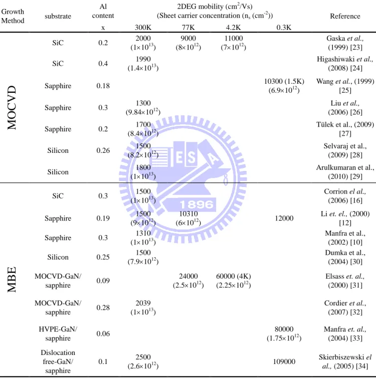
for HEMT applications lately. The main advantages of MOCVD, as compared to MBE, are the high growth rate and high crystal quality material even for the direct growth of GaN layers on the foreign substrates. Besides, MBE has also proven to be a promising technique to grow GaN materials for HEMT devices application [10, 12, 16]. The benefits of growing GaN with MBE include real-time monitoring of crystal growth with reflection high-energy electron deflection (RHEED), a carbon-free and hydrogen-free growth environment, a smooth surface, sharp interfaces and low point defect density. These attributes are important for achieving high quality materials for HEMT devices. Table 1.3 shows some important developments on the electrical properties of AlGaN/GaN structure grown by MOCVD and MBE techniques. Even though the measuring temperatures for the 2DEG mobility are varied for different works, the general tendencies are summarized as following:
(i) AlGaN/GaN structures grown on SiC has the best quality as compared to those grown on sapphire or Si substrates.
(ii) For direct growth of AlGaN/GaN structure on the substrate, MOCVD samples are better than MBE samples.
(iii) For AlGaN/GaN grown on the high quality GaN templates, the MBE samples are better than MOCVD samples.
The results indicate that the AlGaN/GaN structure grown on SiC has the best crystal quality due to the least lattice and thermal mismatches induced by the substrate. On the other hand,
5
the difference for materials grown by MOCVD and MBE can be explained by the relatively poor ability of MBE to reduce the stress in GaN films when grown on the foreign substrates. For MOCVD growth, the transition from a three-dimensional low-temperature (525-600 °C) GaN nucleation layer to a two-dimensional GaN growth on a sapphire substrate during the substrate temperate ramp-up to a higher process temperature (1060-1100 °C) can effectively reduce the stress and improve the crystalline quality of a GaN film [17]. In contrast, the MBE growth process cannot achieve this transition due to the much lower growth temperature (700-800 °C). Therefore, the MOCVD grown samples have a TD density up to 2 orders of magnitude lower than those grown by MBE. However, Table 1.3 shows that the best AlGaN/GaN structures were grown by MBE on the high quality templates. This indicates that the true ability of MBE may be revealed if the stress issue can be resolved. The following section will discuss the most important issues of GaN material grown by MBE technique on sapphire substrate.
1.4 Growth of GaN by MBE on sapphire
1.4.1 AlN buffer layer
For the growth of high quality GaN on sapphire substrate using MBE, an AlN buffer layer is indispensable. Other than acts as a transition layer, the AlN buffer also helps to achieve a Ga-face GaN grown by MBE [18, 19]. The Ga-face GaN has better crystal quality
6
and smoother surface morphology as compared to the N-face GaN [20]. Furthermore, the Ga-face AlGaN/GaN structure also provides the proper polarity to produce an electrical field to induce carrier into the 2DEG channel for the HEMT device.
1.4.2 Growth temperature
The generally used growth temperatures of GaN materials by MBE fall in between 700-800 C. While a lower growth temperature will degrade the crystal quality of GaN film, a growth temperature higher than this will enhance the desorption rate of Ga atoms from the substrate which will significantly reduce the growth rate and increase the Ga source consumption. However, as compared to the theoretically predicted melting temperature of GaN (~2500 C), the MBE growth temperature is significantly lower than that normally required for other compound semiconductors (50~75% of material melting temperature) to achieve high quality single crystal film. The growth of GaN by MBE is therefore occurred under the thermodynamically meta-stable condition with a non-equilibrium kinetically-limited reaction [21].
1.4.3 III-V ratio
The III-V ratio is an important growth parameter for the GaN materials. It is referred as the ratio of active Ga and N atoms that available for the growth under a given substrate temperature. Hence, for an identical supply of Ga and N sources, the III-V ratio will change at different substrate temperatures. III-V ratio not only controls the crystal quality of MBE
7
grown GaN but also significantly affect its surface morphology. The GaN surface morphology is determined by the following three growth conditions [22]:
(i) N-rich: rough surface with cratered morphology
(ii) Intermediate: large areas of uniform and flat surface but having pits and irregular, faceted edges,
(iii) Ga-rich: Smooth surface but with Ga droplets form on the surface.
Optimum growth condition, which is chosen somewhere in between the intermediate and Ga-rich regimes, will offer a smooth surface and without any Ga droplets
1.5 Objective of the study and organization of this thesis
In this study, the growth of high quality GaN material by MBE for the HEMT fabrication is investigated. All the materials were grown on the 2-inch c-plane (0001) sapphire substrate which is relatively cheap and available with high quality.
The thesis is divided into six chapters. The first chapter gives the background of the study. In the second chapter, detail descriptions on the MBE system, experimental procedures and the characterization methods are presented. Chapters 3 to 5 are the experimental results. The dependence of the defect structure of GaN film on the AlN buffer growth parameters was first investigated (Chapter 3). This understanding is important for improving the GaN crystal quality. With this understanding, an effective method by combining the Ga-lean GaN buffer
8
and migration enhanced epitaxy was invented and the growth of high crystal quality GaN film by MBE using this approach will be described in Chapter 4. In Chapter 5, the roles of different dislocation types on the electrical properties of GaN HEMT grown by MBE are investigated. Chapter 6 concludes the study.
9
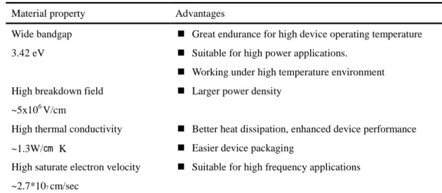
Table 1.1 Advantages of GaN material for electronic applications.
Material property Advantages Wide bandgap
3.42 eV
Great endurance for high device operating temperature Suitable for high power applications.
Working under high temperature environment High breakdown field
~5x10⁶V/cm
Larger power density
High thermal conductivity ~1.3W/㎝ K
Better heat dissipation, enhanced device performance Easier device packaging
High saturate electron velocity ~2.7*107 cm/sec
Suitable for high frequency applications
Table 1.2 Material properties of GaN, AlN, Si, SiC and sapphire.
Material a (Å ) c (Å ) Thermal conductivity (W/cm K) Thermal expansion coefficient (In-plane, 10-6 K-1) Lattice mismatch GaN/substrate (%) Thermal mismatch GaN/substra te (%) GaN 3.189 5.185 1.3 5.59 - - AlN 3.112 4.982 2.85 4.2 2.4 25 Si (111) 5.430 - 1.3 2.59 -16.9 54 6H-SiC 4.9 4.2 3.5 25 Sapphire 4.759 12.991 0.5 7.5 16 -34
10
Table 1.3 Comparison of 2DEG mobility and sheet carrier concentration of AlGaN/GaN
structure grown by MOCVD and MBE on different substrates. MOCVD-GaN stands for GaN template grown by MOCVD; HVPE-GaN stands for GaN template grown by HVPE; Dislocation free-GaN stands for very high quality free-standing GaN template; the carrier mobility and concentration are measured at 300, 77, 4.2 or 0.3 K unless specify in the bracket; x is the Al content in AlGaN layer.
Growth
Method substrate
Al content
2DEG mobility (cm2/Vs)
(Sheet carrier concentration (ns (cm-2)) Reference
x 300K 77K 4.2K 0.3K
MOCVD
SiC 0.2 2000 (11013) 9000 (81012) 11000 (71012) Gaska et al., (1999) [23] SiC 0.4 1990 (1.41013) Higashiwaki et al., (2008) [24] Sapphire 0.18 10300 (1.5K) (6.91012) Wang et al., (1999) [25] Sapphire 0.3 1300 (9.841012) Liu et al., (2006) [26] Sapphire 0.2 1700 (8.41012) Tülek et al., (2009) [27] Silicon 0.26 1500 (8.21012) Selvaraj et al., (2009) [28] Silicon 1800 (11013) Arulkumaran et al., (2010) [29]MBE
SiC 0.3 1500 (11013) Corrion el al., (2006) [16] Sapphire 0.19 1500 (91012) 10310 (61012) 12000 Li et. el., (2000) [12] Sapphire 0.3 1310 (11013) Manfra et al., (2002) [10] Silicon 0.25 1500 (7.91012) Dumka et al., (2004) [30] MOCVD-GaN/ sapphire 0.09 24000 (2.51012) 60000 (4K) (2.251012)Elsass et. al., (2000) [31] MOCVD-GaN/ sapphire 0.28 2039 (11013) Cordier et al., (2007) [32] HVPE-GaN/ sapphire 0.06 80000 (1.751012)
Manfra et. al., (2004) [33] Dislocation free-GaN/ sapphire 0.1 2500 (2.61012) 109000 Skierbiszewski el al., (2005) [34]
11
N
N
N
N
Net fixed polar charges at the AlGaN/GaN interface:
Ppz (AlGaN) + Psp (AlGaN) – Psp (GaN)
(AlGaN)
(GaN)
Fig. 1.1 (a) Polarization effect on the AlGaN/GaN structure. Psp and Ppz are
spontaneous and piezoelectric polarizations, respectively. (b) Carriers at the 2DEG are induced by the surface traps (charges) and polarization field in the AlGaN/GaN structure.
(a)
12
Chapter 2
Plasma-Assisted Molecular Beam Epitaxy System, Experimental Procedure and
Characterization Methods
In this chapter, the plasma-assisted molecular beam epitaxy (PA-MBE) system used for GaN materials growth is introduced. The general procedure for the epitaxial growth will also be described. Finally, various measurement methods that used to characterize the material crystal quality and electrical performances of AlGaN/GaN devices are presented.
2.1 Plasma-assisted MBE system
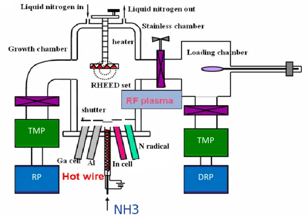
The PA-MBE system was designed by ULVAC Inc. for the epitaxy growth of group III-nitride materials. Both binary and ternary compound materials are grown using the group III sources of gallium (Ga), aluminum (Al) and indium (In) and group the group V source of nitrogen. The following sections describe briefly the important parts of the MBE system.
2.1.1 Chambers and vacuum pumps
The MBE system consisted of two chambers (Fig. 2.1): a sample preparation chamber or loading chamber (LC) and a growth chamber (GC) connected by a gate valve. A dry rotary pump (DRP) and a turbo molecular pump (TMP) are used in the LC. Pressure in the LC has to reach below 5x10⁻⁶ Pa before the sample is transferred into the GC. The GC, which is equipped with a rotary pump (RP), a TMP, a sputter ion pump and a titanium getter pump, has
13
a base pressure <2x10⁻⁸ Pa. However, during the material growth, only the RP and TMP are used to maintain the growth pressure at the range of 5-8x10⁻³ Pa depending on the flow rate of the nitrogen gas.
2.1.2 Sample manipulator and growth sources
Sample holders (molybdenum) are available for 2, 4 and 6 inch substrates. The substrate surface is facing down when it is placed on a sample manipulator which is rotated by an external motor. Substrate rotation up to 10 rpm is applied to improve the deposition uniformity across the wafer. A substrate heater is located just above (behind) the sample holder to control the material growth temperature (up to about 850oC). Four effusion cells are installed for high purity solid sources of Ga, Al (2 cells) and In. Source fluxes emerging from the effusion cell are controlled by the cell temperature (up to 1250oC). Nitrogen source in the form of nitrogen radical is generated by two RF plasma generators. The amount of generated nitrogen radical is affected by the nitrogen gas flow rate as well as the RF power. Beside the plasma generator, nitrogen source from ammonia gas is also available by the installation of a hot-wired „cracking cell‟. All the sources are deployed at the bottom part of the chamber and are co-focused onto the substrate holder (Fig. 2.1). A pneumatically controlled shutter is placed in front of each cell to control the sources used in material growth.
2.1.3 Analytical instruments and others
14
(RHEED) for the real-time monitoring of epitaxial growth. High energy electron beam (20 keV), which is directed onto the sample surface at a grazing incidence (~2 degree), allows a surface-sensitive analysis during the growth.
An ionization gauge mounted at a flange on the chamber wall can be brought forward and place in front of the substrate to measure the source fluxes when necessary. In this way, the ionization gauge acts as a beam flux monitor (BFM) to calibrate the molecular beam intensity from time to time. A quadrupole Residual Gas Analyzer (RGA) is also placed at the rear part of the GC to detect the presence of the impurity gases in the chamber.
Both the growth chamber wall and source flanges are surrounded by liquid nitrogen (LN2)
cryopanels. LN2 is flowed into the cryopanels during the growth process to prevent
re-evaporation of impurities from parts other than the hot cells. The crypanels also provide thermal isolation among different cells.
2.2 Growth procedures
In this section, the general procedure for the growth of GaN material on sapphire substrate is described. The typical growth steps includes: sample preparation, nitridation, growth of buffer layer and growth of GaN epi-layer.
2.2.1 Sample preparation
15
mm) substrates with C-place orientation (<0001>). After loading into the growth chamber, the substrate was first annealed at ~820oC for about an hour to clean the surface. The cleanliness of substrate surface was monitored using RHEED. After the thermal treatment, a clear and sharp RHEED pattern appeared as shown in Fig. 2.2a.
2.2.2 Nitridation
After the thermal annealing, the sapphire surface was treated with nitrogen plasma in the so-called „nitridation‟ process. During the nitridation, the sapphire surface (Al2O3) was
converted slowly into a thin AlN layer. This layer acted as a starting layer for the epitaxial growth of AlN buffer layer. The effect of nitridation process on the crystal quality of GaN epilayer grown by the same MBE system was discussed in a previous study [35]. Without the nitridation process, the grown GaN material has low crystal quality and rough surface morphology. Furthermore, the nitridation temperature and duration are also important for the GaN epilayer growth. A rougher sapphire surface occurred after nitridation at high temperature (800oC) and it could generate more screw dislocations in the GaN film. On the other hand, nitridation performed at low temperature (200oC) would need longer time (90min) to transform the sapphire surface into AlN layer. In this study, substrate temperature of ~600oC and duration of 60min were chosen for the optimum nitridation result. The change of the surface structure of sapphire upon nitridation could be observed using RHEED. As shown in Fig. 2.2, the RHEED pattern of the original structure of Al2O3 (Fig. 2.2 (a)) changed to that
16
of AlN structure (Fig. 2.2(c)) after one hour of nitridation.
2.2.3 Growth of buffer layer
Buffer materials generally used for the growth of GaN on sapphire substrate include low temperature GaN (LT-GaN), LT-AlN and high temperature (HT-AlN). In this study, AlN buffer layer was used. AlN not only improve the material quality of GaN but also help to achieve Ga-face GaN film grown by MBE on sapphire [18, 36]. Ga-face GaN provides polarization charges at the AlGaN/GaN interface for high electron mobility transistor (HEMT) fabrication. The effect of AlN growth parameter on the defect structure of GaN will be investigated in the Chapter 3. RHEED pattern on AlN grown on sapphire after the nitridation is shown in Fig. 2.3 (a).
2.2.4 Growth of GaN layer
The crystal quality of GaN film grown by MBE is determined by several factors such as the growth temperature, III/V ratio and the quality of buffer layer. The growth temperatures of GaN using MBE fall in a wide range from 650-800 C [12, 16, 20, 34]. A higher growth temperature is preferable for better crystal quality but will enhance the desorption rate of Ga adatoms from the substrate. As a result, a larger Ga flux is needed to maintain a reasonable growth rate. On the other hand, the Ga/N ratio is used to control both the material quality and surface morphology of GaN. While a rough and low quality material is formed under the nitrogen rich growth condition, a smooth but with Ga metal droplets left on the GaN surface if
17
too Ga-rich growth condition is used [20, 37]. Therefore, the optimum growth conditions for GaN with good quality and smooth surface (but without the Ga-droplet) can be achieved by the careful control of both the growth temperature and the Ga/N ratio. In this study, the growth parameters of GaN were initially optimized using a homoepitaxial growth approach. The homoepitaxial growth was carried out by depositing GaN film (~1m) on a high-quality GaN film (~2m) grown on sapphire by metal-organic chemical vapor deposition (MOCVD) (referred here as the GaN-template). This approach proved useful for achieving high-quality GaN film by MBE [33, 34]. Under the optimized growth condition, the crystal quality and surface morphology of GaN after regrowth should be identical with or better than that of the GaN-template. For the ULVAC MBE system, the growth parameters used are listed in Table 2.1. The growth rate of GaN is about 0.4 m/hr under this growth condition. After that, the GaN material is grown directly on the sapphire by using an AlN buffer layer. In situ RHEED analysis during the GaN growth is shown in Fig. 2.3(b). The streaky RHEED pattern indicates that the GaN surface has a smooth surface morphology. After the growth was completed and the substrate was cooled down to below 200oC, the RHEED pattern shows a 2x2 surface reconstruction (Fig. 2.3(c)) which indicates that the GaN has Ga-face polarity [38]. The effect of the growth conditions of AlN buffer layer on GaN quality will be discussed in Chapter 3.
18
In this section, the measurement methods used to characterize the material quality and electrical properties of GaN grown by ULVAC MBE system are described.
2.3.1 Field emission scanning electron microscope (FE-SEM)
The FE-SEM consists of a field emission electron source rather than a thermionic emission source used in a Thermal Tungsten wire SEM. A FE-SEM is therefore has a cold cathode. This SEM provides higher resolution imaging with higher beam density (brightness), and longer tip life. The primary electrons enter a specimen surface with energy of 0.5 to 30 keV to generate many low energy secondary electrons. The second electrons emission depends largely on the accelerating voltage of the primary electrons and also the probing incident angle on the specimen surface. In general, a large quantity of secondary electrons is generated from the protrusions and the circumferences of objects on the specimen surface, causing them to appear brighter then smooth portions. Under a constant accelerating voltage, an image of sample surface can thus be constructed by measuring the secondary electron intensity as a function of the position of scanning primary electron beam. In this study, Hitachi S-4700 FE-SEM is used routinely to check the GaN surface morphology as well as the film thickness.
2.3.2 Atomic force microscope (AFM)
AFM is used to check the surface topography of a material by measuring the interaction force between the AFM‟s probe and surface structure. The AFM probe consists of a sensitive
19
cantilever and a sharp tip (tip radius <10 nm) capable of obtaining the detail surface morphology of a material surface on the atomic scale if the scanning condition is carefully controlled. In general, the AFM is reliable to achieve lateral and vertical resolutions down to about 2 nm and 0.05 nm, respectively, in the ambient air environment. In this study, AFM Dimension 3100 system from Digital Instrument was employed to examine the surface information, such as morphology, roughness and density of pits, from the GaN material grown by MBE. This information provides the indications of the material quality and is a useful means to tune the growth condition.
2.3.3 High resolution X-ray diffraction (HRXRD)
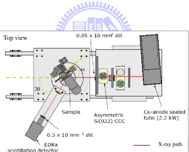
HRXRD is the most powerful and commonly used characterization method to check the crystal quality of epitaxial grown materials. Besides being a non-destructive method, it also requires no sample preparation prior to the analysis. In this study, the Bede D1 HRXRD system (Fig. 2.4) equipped with a high power (2kW) X-ray source of Cu K line was used to
determine the crystal quality of GaN grown by MBE. In additional to the crystal quality, other information of the GaN, such as lattice parameters, Al composition in the ternary compound of AlGaN and the AlGaN thickness were also determined by HRXRD. The following sections describe the frequently used scanning modes of the HRXRD in this study and its applications for epi-layer analysis.
20
Rocking curves were measured by scanning on the sample angle (or Omega) only. Such a scan is suitable for investigating the epi-layer crystal quality. In this study, it is assumed that the broadening of the rocking curve of a certain diffraction plane is mainly caused by the presence of threading dislocation (TD) in the GaN material. Three types of TDs are normally occurred in GaN: screw, edge and mixed TDs. These TDs can be distinguished by having different defect structures or Burgers vector, b. The b for screw, edge and mixed TDs are <0001>, 1/3 <11-20>), and 1/3 <11-23>, respectively. Due to this specific defect structure, the screw dislocation can distort all the (h k i l) planes with l non-zero, while the edge TD can distort only the (h k i l) plane with either h or k non-zero. Therefore, the GaN (0002) plane rocking curve is broadened by screw- and mixed-type TDs, while the GaN (10-12) plane rocking curve is broadened by all TDs [7, 39].
In order to estimate the TD density in the GaN grown by MBE, the rocking curves for both the symmetric plane (0002) and asymmetric plane (10-12) were scanned for each sample. Full-width at half-maximum (FWHM) of the rocking curves was determined by non-linear least-square fitting to a pseudo-Voight function. After that, an approach suggested by Gay et
al. [40] as shown in equation (2.1) was used to estimate the TD density in GaN film:
Ddis ~ 2/ 9b2 (2.1)
where Ddis (unit = cm
-2) is the TD density in the material,
(in radian) is the FWHM of a given XRD peak, and b (Å ) is the length of Burgers vector of their corresponding dislocation. For
21
GaN grown at the <0001> direction, the b of the screw TD is the GaN a-axis lattice constant, i.e. 3.189 Å while the b for the edge TD is the GaN c-axis lattice constant, while is equal to 5.186 Å . To simplify the calculation of dislocation density, the mixed TD was divided into screw- and edge-type TDs [7]. So the “screw TD‟ used in this study was the sum of pure screw-type and the screw component of mixed-type TDs, while the „edge type‟ was the sum of pure edge-type and edge component of the mixed-type TDs. In this way, the rocking curve width caused by the screw and edge TD in the GaN films can be estimated from the (10-12) rocking curve scan using the following equation:
(10-12)2=s2+e2 (2.2)
where (10-12) is the FWHM of (10-12) plane, and s and e are the contributions of screw and
edge TDs to the FWHM of (10-12) plane, respectively. Using equations (2.1) and (2.2), the screw and edge TD densities of GaN can be calculated. For example, if the GaN film grown by MBE showing the (0002) and (10-12) rocking curves of 100 and 1000 arcsec, respectively, then the estimated screw and edge TDs are 9.71x10⁶ and 2.54x109 cm-2, respectively.
2.3.3.2 Omega-2theta (-2) scan
-2 scan was performed by scanning the sample and detector angles together in a 1:2 ratio. Such a scan is usually used to check the sample which contains thin and lattice mismatched layers. Diffraction signals from layers with different lattice constants along the diffraction plane will appear at different scanning angles. -2 scan is therefore useful to
22
compare the relative change in lattice constant due to residual stress or composition variation. In this study, -2 scan was normally used to determine the Al composition in the AlGaN layer grown on GaN layer. Thickness of AlGaN can also be calculated from the simulation and data fitting from the -2 scan.
2.3.3.3 X-ray reflectivity (XRR) scan
XRR is performed at a grazing incidence beam is suitable for studying surface and layers near the sample surface. By fitting the scanned patterns, layer information such as film thickness, surface and interface roughness can be obtained. This is especially useful for the top layers with thickness less than a few hundreds of nm and roughness less than 35 Å (root-mean-square). Even though the thin layer can either be single crystal, polycrystalline or amorphous material, XRR is always used in this study to determine the thickness of the thin AlGaN or AlN/AlGaN layers (<30 nm) which grown on top of the GaN film.
2.3.3.4 Reciprocal space mapping (RSM)
RSM is used to distinguish the strain and tilt in a sample. A series of scans of -2 at different offset angles is performed and then converted into a map of diffraction intensity in the reciprocal space. RSM can be performed on both symmetric and asymmetric planes. When a RSM is performed on the symmetric planes of the substrate and an epilayer, the tilt angle of the epilayer with respect to the substrate can be observed. Besides, the relative out-of-plane lattice parameter of these two materials can also be calculated. Meanwhile, when
23
a RSM of the asymmetric planes is obtained, both the relative in-plane and out-of-plane lattice parameter of the substrate and epilayer can be calculated. In this study, the RSM of asymmetric plane (such as (10-15) plane) was scanned occasionally to determine the strain and the Al composition of the thin AlGaN layer grown on the GaN film.
2.3.3.5 Triple axis diffraction
The few HRXRD modes described above are performed under the double axis configuration, i.e. without an analyzer crystal being installed at the detector stage. On the other hand, if an analyzer crystal is used as in the triple axis configuration, the acceptance angle of the detector was reduced to a few arcsec, allowing a finer definition of the scattering angle, 2. With such a high accuracy, the deflection angle from a certain crystal plane can be used to calculate the lattice constant of the scanned material. In this study, the triple axis configuration was used to determine the c-axis lattice constant of the GaN by obtaining the 2 value of the (0002) plane.
2.3.4 Transmission electron microscope (TEM)
TEM is the powerful tool to characterize the epitaxial layer microstructure. Operating on the basic principles of the optical microscope, the TEM takes the advantage by using electron beam source which has much shorter wavelength as compared to the optical source. Therefore, the resolution of TEM can reach to about 0.2 nm, in the ideal imaging condition, in contrast to an optical microscope which can only reach to 200 nm. Besides the imaging capability, the
24
TEM is also equipped with other analytical tools such as energy dispersive spectroscopy (EDS) and electron energy loss spectroscopy (EELS) for material chemical composition analysis. In this study, the JOEL 2010F TEM system operated at 200 kV was used occasionally to check the crystal quality and microstructure of the GaN grown by MBE. Besides, the TEM was also employed to study the dislocation bending behavior in the GaN as a function of the buffer layer growth parameters. For sample preparation, the GaN/sapphire materials for TEM analysis were prepared either by focused ion beam (FIB) or conventional mechanical polishing and followed by an Ar-ion milling process.
Since the GaN materials grown in this study were meant for the fabrication of high electron mobility transistor (HEMT), the electrical properties of the grown materials therefore needed to be characterized. Some important characterization methods include the Hall effect measurement, the capacitance-voltage, current-voltage and direct electrical current measurements are briefly described below. All the samples for Hall measurement and for both the SBD and HEMT devices were fabricated using in-house facilities.
2.3.5 Hall effect measurement
The Hall effect measurement is an important characterization method for the semiconductor materials in determining the electrical resistivity, carrier density, carrier types
25
and the mobility. In this study, the grown material structure for HEMT fabrication consisted of a thin AlGaN layer on the GaN film. Such a structure generates a 2-dimensional electron gas (2DEG) at the interface, which plays the most important role in the HEMT devices. The electrical properties, such as sheet resistivity, sheet electron density and electron mobility of the 2DEG were regularly determined by the Hall effect measurement system (Bio-rad HL55Win). The measurements were conducted in a Van der Pauw (VDP) configuration at room temperature.
2.3.6 Capacitance-voltage (CV) and current-voltage (IV) measurement
Schottky barrier diodes (SBD) with a circular Schottky contact surrounded by an ohmic ring were prepared for the CV and IV measurements. The CV measurements can be used to determine the charge concentration in the AlGaN/GaN structure as a function of depth from the material surface (estimated from the applied depletion voltage). Therefore, it is useful to check the carrier density in the 2DEG channel or the presence of carrier in the buffer layer of the AlGaN/GaN structure. On the other hand, the IV measurement on the SBD can be performed by applying the Schottky contact with different biases, from positive to negative as relative to ohmic contact. The measured current from the Schottky contact during the negative bias is of particular interest because this implies the leakage current through the AlGaN barrier layer. In this study, the CV and IV on the SBD were measured using an HP4284A LCR meter and a Kethley 4200 semiconductor analyzer system, respectively.
26
2.3.7 Direct electrical current (DC) measurement
After the fabrication of HEMT device on the AlGaN/GaN structure, DC measurements were carried out using an Agilent E5270 system. These include the measuring of drain currents at different drain voltage (Id-Vd), the transconductance (Gm=dId/dVg) and the
threshold voltage (Vth). The Id-Vd values depend on the carrier concentration and mobility of
the 2DEG while Gm reflects the gate modulation ability and higher value is required for high
frequency applications. Another important parameter for the HEMT devices is the off-state breakdown (BVoff). BVoff is determined by the breakdown voltage (defined as Id > 1 mA/mm)
measured by fully depletion of the channel (2DEG in the case for AlGaN/GaN) charges. High value of BVoff is required for high power HEMT operations.
27
Table 2.1 The optimized growth parameters of GaN using ULVAC MBE system.
Growth temperature (oC)
Nitrogen plasma (RF power, N2 flow rate)
Ga flux (partial pressure, Pa) 740 GUN1: 450W, 4.0sccm
GUN2: 450W, 1.5sccm
4.8x10⁻⁵ (b)
28
Fig. 2.1 Schematic diagram of the PA-MBE system.
TMP TMP DRP RP In cell N radical (c)
Fig. 2.2 RHEED pattern of sapphire substrate (a) before nitridation, (b) after 30min
nitridation and (c) after 60min nitridation.
29
Fig 2.3 RHEED pattern of the surface of (a) AlN, (b) GaN during growth and (c)
GaN after cooling to <200oC.
(a) (b) (c)
Fig. 2.4. Schematic diagram of the BEDE D1 HRXRD system.
Top view
X-ray path 2
30
Chapter 3
The Effect of AlN Buffer Growth Parameters on the Defect Structure of GaN
Grown by Plasma-Assisted Molecular Beam Epitaxy
3.1 Introduction
For GaN grown on sapphire substrate using MBE, an AlN is necessary to achieve a high crystal quality Ga-face GaN. The Ga-face GaN is also required to provide the proper polarity to induce carrier into the two-dimensional electron gas (2DEG) at the AlGaN/GaN interface for HEMT device fabrication. Despite the use of AlN buffer, GaN grown on sapphire is still associated with high dislocation density (~1010 cm-2). Intensive studies and various approaches have been carried out to reduce the dislocation density in GaN, however, little is known about the relationship between the different kinds of defect structures. In this chapter, the dependence of different kinds of dislocations on the growth parameters of AlN buffer is investigated. The understanding of their relationship can be used to reduce the total dislocation density in GaN.
3.2 Experiment procedures
Prior to the growth of AlN buffer layer and GaN films, standard high temperature annealing and nitridation processes were carried out as described in Chapter 2. AlN buffer layers of different growth temperatures (from 450 to 840 oC) and thicknesses (from 4 to 30nm)
31
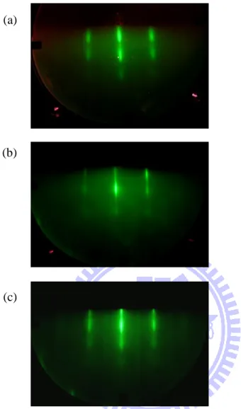
were prepared for the deposition of a 2-m GaN film grown with constant growth parameters. In the first part of these experiments, AlN with constant thickness of 15 nm was used. Six samples (labeled as A-F) were prepared as shown in Table 3.1. In situ RHEED was used to monitor the growth of the AlN and GaN films. RHEED patterns on all the GaN films grown in our experiment were streaky indicating a flat surface (will be determined later) during growth and showing 2x2 surface reconstruction upon cooling (indicating a Ga-face polarity [38]) as shown in Fig. 3.1. On the other hand, the RHEED pattern for AlN was somewhat less streaky indicating that their surfaces were less smooth as a result of lower than unity Al/N ratio was used [41]. This ratio was chosen to avoid the formation of Al droplets on the AlN and cubic face GaN at the hetero-interface which could deteriorate the GaN quality [6, 41].
3.3 Results and discussion
3.3.1 Influence of growth temperature
Defect structures of the GaN films were determined by high resolution x-ray diffraction (HRXRD). Using double-axis configuration, the rocking curves (-scans) for both the symmetric plane (0002) and asymmetric plane (10-12) were scanned for each sample. Full width at half-maximum (FWHM) of the rocking curves was determined by non-linear least-squares fitting to a pseudo-Voight function. Table 3.1 summaries the rocking curve widths of GaN (0002) and (10-12) planes grown on different growth temperature AlN buffers.
32
As shown, the (10-12) FWHM was reduced with the increase of (0002) FWHM. Or in other word, the reduction of the total dislocation density in GaN film was associated with an increase of screw or mixed TDs when lower temperature AlN buffers were used.
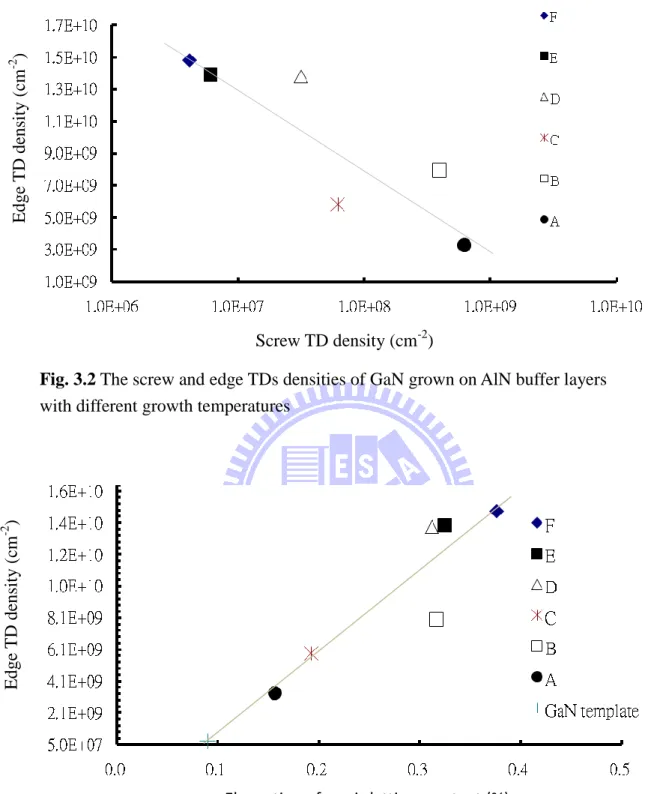
The dislocation densities in GaN film were estimated from the HRXRD method as described in Section 2.3.3.1. Both the screw and edge TD densities of GaN were calculated and the results are plotted in Fig. 3.2. This figure clearly shows that the edge TD density in GaN film was reduced with the increase of screw TD density. In general, GaN film grown on lower temperature buffer have a lower edge TD density and higher screw TD density than GaN films grown on higher temperatures buffer. Even though the edge TD is dominated in all cases, consistent with previous studies of MBE-grown GaN [6] [39], it can be effectively suppressed with the use of a buffer layer grown at lower temperature. The edge TD density reduced from 1.5x10¹⁰ to 3.3x109 cm-2 when temperature was decreased from 840 to 450 oC. Since the edge TD densities were at least an order of magnitude larger than that of the screw TD (except sample F), the total TD density was also reduced at the similar trend (from 1.5x10¹⁰ to 3.9x109 cm-2) despite a significant increase of the screw TD density in the film.On the other hand, the generation of screw TD was restricted by using higher temperature buffer layers. Screw TD density as low as 4.1x106 cm-2 was achieved for GaN film grown on the 840
o
C AlN buffer.
33
Further study was carried out to investigate the correlation between defect structure in GaN films and growth temperature of AlN buffer. It is well known that the residual stress can cause the formation of dislocation in a material. Thus the stress in GaN is also believed to have played a role to manipulate the defect structure in it. The stress in our GaN film was determined by measuring the strain in the GaN lattice constants. Because the GaN epilayer grown on sapphire exhibits in-plane isotropic elastic properties, its in-plane stress () can be described by the lattice strain () from the relationship: = M, where M is the biaxial elastic modulus of GaN. In order to accurately calculate the stress in GaN film grown on sapphire, however, more comprehensive XRD surveys on various asymmetric planes are needed [42]. In this study, the stress states in GaN films were represented by the deformation of its c-axis lattice constants (c). When the hexagonal GaN film is biaxially stressed on sapphire, its
in-plane lattice deformation (a) is associated with out-of-plane lattice change as described by
the relationship: c -a. Thus, the stress states in the GaN can be illustrated from the
deformation of its c-axis lattice constant. Using triple-axis configuration from the same x-ray diffractometer (as described in Section 2.3.3.5), the deflection angles of (0002) plane were obtained with high accuracy (within a few arcsec) to determine the c-axis lattice constant of GaN films grown on different temperature AlN buffers. Fig. 3.3 shows that the edge TD density was increased proportionally with the strain in the GaN film. All the films were compressively stressed with their c-axis lattice constants elongated to different degrees.
34
Increment of the edge TD density from 3.3x10⁹ to 1.5x1010 cm-2 corresponded to the elongation of the c-axis lattice constant from 0.15 to 0.38 %. Therefore, the result reveals that the stress in the GaN film has a significant influence on the edge TD as well as the total defect density. For comparison, the data for GaN film grown on the Ga-template (total thickness of about 1 m) is also shown in Fig. 3.1. The edge TD density of this sample was only 2.5x108 cm-2, with the c-axis lattice constant elongated to merely 0.09 %. This means that the GaN grown on the GaN-template has the least inherent stress and, thus, the best crystal quality.
From the result shown in Fig. 3.2, it appeared that the screw and edge TD densities were controlled by the properties of AlN buffers. To clarify this, we have carried out another set of experiment to grow only the AlN buffer layers on sapphire without GaN films on them. The growth procedure was identical to that described before. After the AlN buffers with nominal thickness of 15nm were deposited at temperatures shown in Table 3.1, substrate temperatures were briefly increased/ decreased to the growth temperature of GaN before it were cooled to room temperature. The crystal property and the surface morphology of these AlN buffers were characterized using XRD and AFM, respectively. Here, due to weak signals from the thin AlN layers, only rocking curve of its symmetrical (0002) plane was scanned. It was surprisingly to find out that the width of (0002) rocking curves of all the samples were almost the same, varied between 119 and 128 arcsec, without a clear changing trend against their growth temperature. The small variation in rocking curve widths has suggested that the crystal quality
35
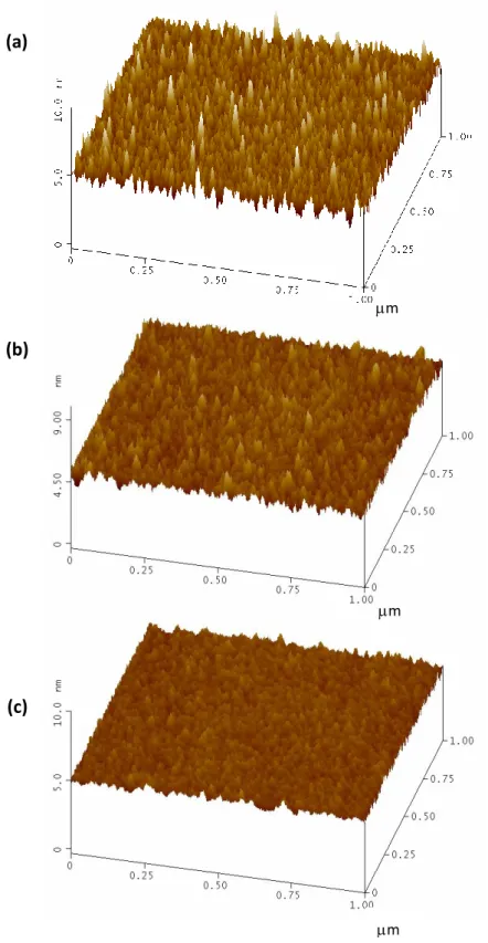
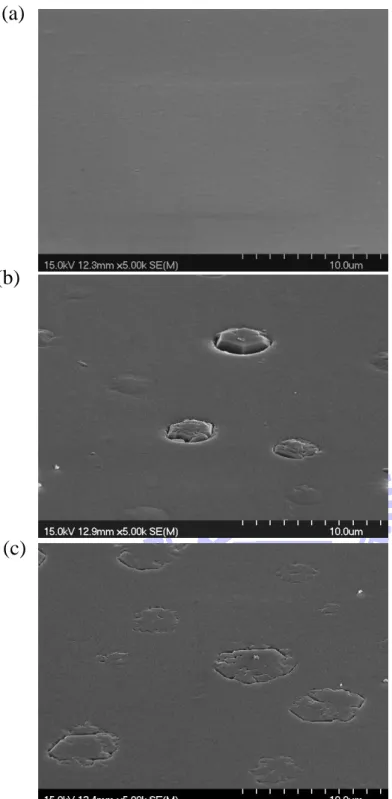
of AlN was not affected by the different growth temperatures used in this study. However, results from the AFM scans have shown that the surface roughness of AlN layers was decreased gradually when the growth temperature was increased in the experiment. In Fig. 3.4, three representative AFM images show that the surface roughness (rms) of AlN grown at 450, 740 and 840 oC were 0.42, 0.29 and 0.19 nm, respectively. For AlN grown at lower temperature, the shorter diffusion length of Al atoms was seemed to create more nucleation sites on sapphire when they were reacted with the nitrogen radicals. The AFM images also show that the density of these “nuclei” was larger on a lower temperature AlN surface. These results, thus, imply that the distribution of different defect structures in the GaN was influenced by the surface roughness of AlN buffer layer. Higher screw TD density was generated in the GaN film when grown on the rougher AlN buffer surface. This is agreed with the finding of Shen et al. [43], which has suggested that the small nuclei on AlN buffer were the origin of spirally growth features that further developed into screw TD in the GaN film. On the other hand, the edge TD density was reduced with the AlN surface roughness. This phenomenon will be discussed later.
In view of the different roughness in AlN buffers deposited at different temperatures, we have also investigated the surface morphology of GaN films grown on them. SEM images (Fig. 3.5) show that the surfaces of GaN films were flat for samples C to F (with AlN buffer temperatures increased from 525-840 oC, only image of sample C was shown in Fig. 3.5 (a)).
36
The surface roughness (rms) of sample C (roughest among the samples C to F) was 0.56 nm on a 1x1 um2 area. However, for GaN films grown on AlN buffers lower than 525 oC, some hexagonal shape features were appeared on the GaN surfaces as shown in Fig 3.5 (b) and (c) for sample B and A, respectively. These features could most probably be related to the screw or mixed types TDs which are always grown following a spiral course into a surface hillock with hexagonal boundary [20, 44]. Some of these features were quite large (3-4 microns) and with hexagonal-like polygon boundaries, especially for those on sample A. This might caused by the clustering of many screw/mixed TDs grown in the close vicinity. Therefore, it is believed that these features were the consequences of rough AlN surface grown below 525 oC and high screw/mixed TD (>108 cm-2) in the GaN film.
3.3.2 Influence of AlN thickness
In this study, it is particularly interested at the formation origin of edge TD, which is dominant in GaN grown by MBE and more deleterious to the material electrical properties. As seen before, the edge TD was closely related to the stress in GaN film which controlled by the growth temperature of AlN. Now, we would also like to see the effect of AlN thickness on the edge TD in GaN films. AlN grown at 525 oC with relatively lower edge TD density and smooth surface has been chosen to further investigate the influence of buffer thickness on the edge TD density. GaN grown on AlN deposited at 525 oC but with different thicknesses (from 4-30nm) were prepared. The changes of both GaN edge TD density and lattice strain on AlN
37
thickness were illustrated in Fig. 5.6. As shown, the lowest strain and lowest edge TD density were achieved on a 15-nm thick AlN buffer. This value is comparable to those reported by other groups (~20 nm) for optimized GaN quality [10, 12]. Besides, the screw TD densities were about the same for all these samples (~6x107 cm-2, not shown here). For GaN grown on sapphire by MBE, AlN is always used to achieve Ga-face GaN. Although AlN has a lattice constant intermediate between film and substrate, it is physically harder and thermally more stable than the GaN buffer which is normally used in metal-organic chemical vapor deposition (MOCVD). The stress in the GaN film is therefore more difficult to relax when an AlN buffer is used. A survey done by Pankove et al. [45] has shown that GaN grown on AlN buffer experienced larger stress than GaN grown on a GaN buffer. Therefore, a MBE grown sample is always associated with larger stress than those grown using MOCVD. It is thus logical that larger AlN thickness will induce larger stress values in the GaN [46]. Unexpectedly, however, larger stress is also encountered in GaN film grown on AlN thinner than 15nm (Fig. 5.6). More studies should be conducted to understand the stress-relaxation mechanisms caused by AlN buffer layer.
From all the above findings, we would now wish to discuss the effect of AlN growth parameters on the formation of edge TD and residual stress in GaN. For GaN grown on sapphire, the large stress generated should be relieved through the formation of misfit dislocation (at the materials interface) and/or plastic deformation in the crystal (achieved with