A Voltage-Mode Controlled High-Input-Power-Factor AC Line
Conditioner with Minimized Output Voltage Harmonics
Yu-Kang LO Chern-Lin Chen
Dept. of Electrical Eng. National Taiwan University
Taipei, Taiwan, R.O.C.
Abstract - A new AC line conktioner is presented. Th~s system consists of a high-input-power-factor half-bridge switch-mode rectifier, DC-lmk capacitors and a low- output-harmonic half-bridge inverter. The rectifier is operated under voltage-mode feedback. No current sensing is required. The inverter is controlled by an EPROM-based modulator. Optimized SPWM patterns compensating DC- llnk voltage ripple and dead time effects are programmed. Synchronizing the SMR and the inverter can eliminate the voltage imbalance between DC-lmk capacitors. The presented system is feasible for single- and three-phase applications.
INTRODUCTION
More and more modern industrial applications require stable single- or three-phase AC power sources while the utility systems are contaminated by increasingly proliferated power electronics equipment. The demands for AC line conditioners providing high-quality AC output power are rapidly growing. The line conditioners usually consist of AC/DC diode-bridge rectifiers, DC-lmk capacitors and DC/AC PWM inverters. Diode rectifiers usually produce serious line current distortion. Bulky filter capacitors are utilized to remove the low-order line-frequency voltage harmonics on inverter's output. System dynamic response is inevitably slow. Switch-mode rectifiers ( S M R ) have been proposed recently[ 1-31, Their advantages include unity power factor, lower current harmonics, smaller size of capacitors and regulated DC-lmk voltage. For S M R control, current-mode feedback is more popular than conventional voltage-mode. However, the current-mode technique has the following disadvantages[4] :
1)Current sensing adds complexity and cost to circuit implementation.
2 ) Slope compensation is necessary for peak inductor current control and leads to decreased current control loop gain. 3) Varying switchmg fiequency in hysteresis control causes serious EMI problems and dead zones in the zero crossings of the current waveforms.
In thls paper, a new AC line conditioner is presented as shown in Fig. 1. The three-phase line conditioner for hgh-power applications is built by simply paralleling
'
single-phase systems. T h s line conditioner consists of a hgh-input-power-factor half-bridge switch-mode rectifier, DC-link capacitors and a low-output-harmonic half-bridge inverter, The rectifier is operated under voltage-mode feedback[5]. There are only voltage control loops for input power factor correction and DC-link voltage regulation. No current sensing is required. The inverter is controlled by an Illy-digitized EPROM-based PWM modulator. Optimized SPWM patterns compensating DC-lmk voltage ripple and dead time effects[6,7] are programmed. T h s approach featuring low cost, simple implementation and control is especially suitable in fixed-kequency applications. Synchronizing the SMR and the inverter can eliminate the voltage imbalance between DC-link capacitors
r
Q
AC 14+
olp - I I I (a> (b)Fig.1 Half-bridge AC line conhtioner (a) 14 (b) 34 VOLTAGE-MODE CONTROL OF HALF-BRIDGE S M R
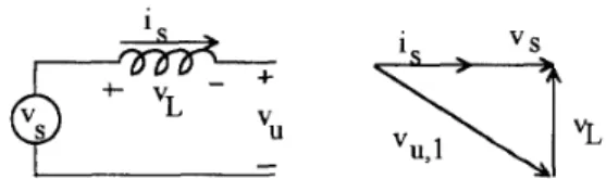
A general circuit for 14 SMR is proposed in [3], as shown in Fig. 2 . vu is the pulse voltage whch could be E or -E depending on the switchmg states. E is the dc voltage of the output capacitor and v , , ~ is the fundamental component of vu.
I-kl
Fig. 2 General circuit and phasor diagram for
14
Sh4RFrom the phasor diagram, the principles of the voltagae- mode control are deduced as follows :
Let v, (t) = h V , sinot, is (t) = h I , sincot under steady state, vL(t) = L dr,(t)/dt =
fi
wLI, cosot, then v,,(t) =fi
(V; sinot-wLI; coswt). From the transfer characteristics of the SPWM inverter and the theorem of superposition, to produce an ac voltage vu,, , the reference signal or the control voltage has to be : I
Jjl OLI,
v,,~~,, = vu,, / E = sinot
-
7
cosot = k, * sinat - k, cosatThat is, the control voltage can be generated by summing an in-phase component and an in-quadrant component. k, is the parameter conceming the feedforward input voltage v,
and k, concerning the feedback output voltage E.
The discussions above are based on the ideal sinusoidal source voltage. If the circumstances are under a distorted source voltage, the deduction is the same except for replacement of the pure sine-term. That is, v,,~,, = k,' v,(t)- k,cosot. Since the dormation about the source voltage is revealed in the first term of vconbo,, a sinusoidal input current can be obtained even with the distorted source present. The block diagram depicting the voltage-mode control for SMR is shown in Fig. 3 .
U
Fig. 3 Block diagram of voltage-mode control
SELECTIONS OF L AND
c
The input inductor can be designed by analyzing Fig. 4(a). Because of the sinusoidal variation of the input current, its switchtng ripple varies period by period. The current ripple can be defmed as the average current variations in a switching period : AI = [(dVdt),,;T,,,
+
(dUdt),,;TS,,,]/2. (dVdt),",, and (dydt),,, are the increasing and decreasing rates of input current. TsON and TsOF are the on-time and off-time of the switch, respectively. By specifying theoL =
A'- (2PN,)'
P is output power, A = (P.r,-nq.E) / (25.lc*V,Z ),
switching frequency
= vs + 2.Ez/vs ' mf= hndamental frequency'
The design of output capacitor is according to the output switching current, as shown in Fig. 4(b). Assuming that a dc current is fed to the load, then I,' contains only harmonics of I,. It is known that the 2nd-order he-frequency harmonic, Io,z , is the dominant one. The capacitance can then be determined as : AV,= I,,z I WC = V, r,% ,
OC = 100 Io.z / (V;ry).
V, is the output voltage, whch is 2-E in the half-bridge topology. Io Idc 4 -Power Circuit (a> (b)
Fig. 4 Selections of (a) input inductor and (b) output capacitor
COMPENSATION TECHNIQUES FOR INVERTERS
With low-order line-fiequency ripples on the DC-lmk voltage, typically-utilized sinusoidal PWM (SPWM) techmques will produce unwanted low-fiequency harmonics in the inverter's output. Assuming that the DC-lmk voltage, V,, , is ripple-free. Then the output of the inverter is an AC voltage modulated by a modulation function with frequency spectrum as depicted in Fig. 5. Harmonics are centered around the multiples of the switchmg fiequency. This AC output can be written as :
Vac= V,,.[m;sinwt +
where ma is the amplitude modulation index and mf is the frequency modulation index. (q* n+k) is the amplitude of the corresponding (rrq.nkk)tlporder harmonic. By filtering out the hgh-order harmonics, a fundamental AC voltage, V,, .m;sinot , can be obtained.
xn+k=odd 1 (m,' nkk)sin((m,-rWwt)l,
T
I
1 mf 2mf
Let's now consider the case in whch low-order harmonic k*h(ot) is superposed on the DC-link voltage, V,, = V,, (l+k*h(ot)). The modulated AC output voltage then becomes :
Vac' = V,, (l+k*h(ot))[m;sinwt +
C"+k=odd 1 (m,* ~ k ) s i n ( ( m f - ~ k ) w t ) ]
Low-order output harmonics are produced due to the multiplication of two low-order terms, k*h(ot) and m;sinot.
= Vac + V,;k*h(ot) masinat
+
1
m,.siriot
By modifying the original reference function to - , the effects of low-order ripples can be removed.
For a bridge-type inverter, a short period of time is always included in control signals between turning one switch in an inverter leg off and turning the other one on. T h s is referred to the "dead time" whch prevents two switches of an inverter leg f?om simultaneous conduction It has been found that the dead time causes a reduction in the fundamental component of the output voltage and introduces low order harmonics which should not be present. A load- current-dependent compensation method[7] can eliminate the output voltage harmonic distortion due to dead time effects. The principles of the compensation techmques are summarized here. When the load current is positive, the timing of the triggering signals to the upper switch in an inverter leg coincides with the ideal control patterns. This can be acheved by turning off the lower switch in advance and turning it on after a delay time. Conversely when the load current is negative the firing signals to the lower switch coincide with the ideal requirements. In t h ~ s way the output AC voltage waveform is almost the same with the original SPWM control patterns. An example of switclung waveforms for dead time compensation is shown in Fig. 6.
I I I
e
1
I
I
1 - 1f
Fig. 6 Switching waveforms for dead time compensation a = ideal triggering signal for upper switch
b = ideal triggering signal for lower switch c = control signal for upper switch when current > 0 d = control signal for loser switch when current > 0
e = control signal for upper switch when current < 0 f = control signal for lower switch when current > 0 Vo = resulted AC output voltages
~
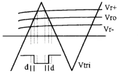
The above method is impossible to implement on the exiting system because it requires primary generation of control patterns for switches in advance. Here a scheme adopting reference sinewaves with offsets is proposed. As shown in Fig. 7, while comparison between V, and V, produces the origmal SPWM signals, comparing V, with V, and V, can give control signals with dead time compensation. The added dc-offsets can be related to the minimum required dead time, d,,,,,, , as :
I
AVI
= V,-
d,,(4fS+o,mJ , where f, is the switchmg ftequency and ma is the amplitude modulation index (see appendlx 2).Fig. 7 SPWM with offsetted reference signals
EPROM-BASED SPWM MODULATOR Conventionally, control signals fed to the PWM inverters are produced by electronic hardware or microprocessor. The cost and complexity of hardware implementation are considerable. On-line computation in the microprocessor approach is laborious and time-comsuming. These two approaches seem impractical when applied to the proposed compensation techniques. An EPROM-based SPWM modulator[8] can solve the problems mentioned above. The SPWM control patterns are pre-calculated by computing the intersections of a reference wave and a triangular carrier wave with numerical method. To program the analogue SPWM patterns into the EPROM, each pulse is composed of several consecutive digital '1's to represent its width. The duration between pulses are represented by consecutive '0's. T h s digitized SPWM pattern can then be retrieved sequentially by incrementing the address counter with a clock. This modulator features the advantages of low cost, fast response, simple control and implementation.
In the proposed EPROM-based modulator for fixed- frequency inverters, an optimized SPWM switchmg function compensating DC-lmk voltage ripple and dead time effects can be off-line calculated and pre-programmed. A fixed- frequency oscillator with counters retrieves the PWM patterns by counting through the addresses of the EPROM. A reset signal is sent at the end of a programmed period from the EPROM to ensure a complete cycle. The block diagram of the proposed modulator is illustrated in Fig. 8.
The fixed-frequency oscillator can be replaced by a traclung PLL circuit when the line ftequency varies
*clear
'
Load current direction
< /
Fig.8 Block diagram of the proposed high-performance EPROM-based SPWM modulator
RESULTS AND DISCUSSIONS
Simulatibns have been performed on the 14 AC line conditioner with the following operating conditions :
Source voltage V, = llOV(rms), 60Hz. AC-side impedance
OL
= 5QDC-lmk capacitance OC = 0.8 1/!2
Output power P = 1kW
Regulated DC-link voltage = 400V Switching frequency = 2kHz
Amplitude modulation index m, = 0.78
Fig. 9(a) shows the input current of
19
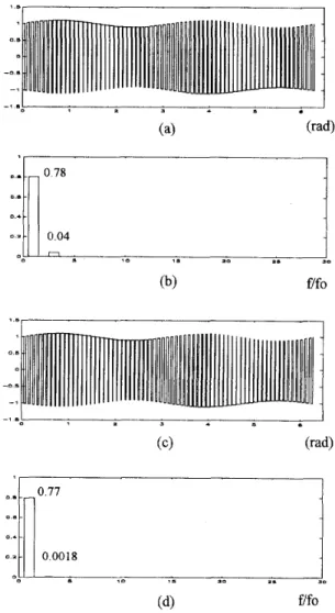
Sh4R. Fig. 9(b) is the output voltage and Fig. 9(c) is the spectrum of input current (THD=8.32%). The switchmg fiequency is set to 2kHz for visual clarity. If a realizably higher switching fiequency, say, 20&, is adopted, the THD is 1.65% whch is well w i t h the maximum allowable limit of 8% in JEEE-5 19. 20, I -20 I 90 95 100 105 110 115 120 125 130 (rad) 405 I I -_.. 90 95 1 W 105 110 115 120 125 130 (b) (rad) r-- '--1 (c) WfoFig. 9(a) Input current (b) Output voltage (c) Spectrum of (a)
is the spectrum without compensation. Fig. lO(c) and (d) show those with compensation. The differences between Fig. lO(a) and Fig. 1O(c) are not obvious since the compensation is revealed in the high-fieqyency modulation function. However, in Fig. 10(d) the 3rd harmonic is reduced greatly compared to that in Fig. lo@). By filtering out the harmonics which are multiples of the switching frequency, qualified AC outputs can be supplied to the loads. --1.- 1
.
J 'I I - 0 s - 14n"'77
Fig. 1 O(a) Normalized output voltage without compensation (b) Spectrum of (a)
(c) Normalized output voltage with compensation (d) Spectrum of (c)
20,
I
-20
'
l18 20 22 24 26 28 30 32
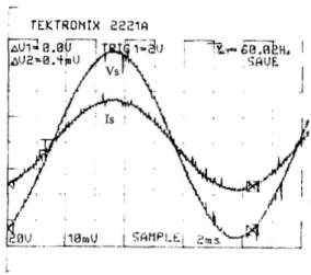
Fig. 11 Input currents of 341 SMR (rad) In the laboratory experiments, a 1+ half-bridge S M R is built and the results are recorded. Illustrated in Fig. 12 is the input current and input voltage under voltage-mode control. The source voltage (SOVrms, 60Hz) is supplied by an AC power supply. Input inductance and output capacitance are
2.6mH and 1 lSO@, respectively. Switching fiequency is 50k.H~ and a 667Q resistive load is used. Output DC voltage is 200V.
?
' TEKTRONIX 2221A
i
Fig. 12 Input voltage and input current (20V/div., 1 Ndiv.)
Shown in Fig. 13(a) is the SPWM control signals fed to switches when the load current is positive. The upper part is the same as the original pattem. The lower part advances turning-offs and delays turning-ons to implement dead-time compensation. Fig. 13(b) depicts the SPWM control signals when load current is negative. The upper part advances turning-offs and delays tuming-ons and the lower part is the original pattem.
In the half-bridge S M R , C1 charges and C2 discharges in ,the positive half-period, and vice versa. This causes the voltage imbalance between C1 and C2. In the proposed AC line conditioner, S M R charges/&scharges and inverter dischargedcharges the same capacitor. In th~s way, the voltage imbalance problem can be solved by synchronizing the SMR and inverter stages.
T E K T R O N I X 222'1A 1
1-.
1 i T E K T R O N I X 2221A II
Fig. 13 SPWM control signals for inverter switches when (a) load current > 0 (b) load current <O
CONCLUSION
A novel control scheme for a new AC line con&tioner is presented. In this scheme, a half-bridge SMR with voltage-mode control serves as the ACDC converter. No inner current loop is required. Based on the principles of the well-developed SPWM, relative circuit simplicity, low cost and regulated DC-link voltage can be acheved. The DCIAC inverter is also a half-bridge type. A fully-digitized SPWM modulator with compensation of DC-link voltage ripple and dead time effects is utilized. Synchronizing the S M R and the inverter can eliminate the voltage imbalance between DC-lmk capacitors. High power capability or
proposed scheme provides a potentially effective and economic way to improve the performance of line conditioners.
REFERENCES
[l] P.
N.
Enjeti and R. Martinez, "A high performance single phase AC to DC rectifier with input power factor correction," IEEE, APEC '93, Conf. Proceedings, pp. [2] N. Mohan, "A novel approach to minimize line-current harmonics in interfacing power electronics equipment with 3-phase utility systems," IEEE Summer power meeting, paper 92 SM 498-6 PWRD, Seattle, WA, July [3] J . C. Salmon, "Circuit topologies for single-phase voltage-doubler boost rectifier," IEEE PESC '92 Proceedings, pp. 549-556.[4] L. D. Salazar and P. D. Ziogas, "A novel current-assisted output voltage control technique for switch-mode- rectifier converters," IEEE Trans. Power Electronics, [5] J. W. Dixon and B. T. Ooi, "Inhect current control of a unity power factor sinusoidal current boost type three-phase rectifier," E E E Tran. Ind. Elec., Vol. 35, [6] P.
N.
Enjeti, W. Shireen, " A new techtuque to rejectDC-link voltage ripple for inverters operating on programmed PWM waveforms," IEEE Trans. Power Electronics, Vol. 7, No. 1 , pp. 171-180, Jan. 1992. [7] R. C. Dodsin, P. D. Evans, H. T. Yazdi, and S . C.
Harley, 'I Compensating for dead time degradation of
PWM inverter waveforms," IEE Proc., Vol. 137, Pt. B, [SI Y. K. Lo, C. L. Chen, J. S. Lin and J. Y. Wu, "A new high-performance AC-to-AC conversion system," IEEE, E C O N '93, Conf. Proceedings, pp. 824-829.
190- 195.
12-16, 1992.
Vol. 7, NO. 3, pp. 444-452, July 1992.
NO. 4, pp. 508-515, NOV. 1988.
NO. 2, pp. 73-81, Mar. 1990.
APPENDIX 1
From Fig. 4(a), the maximum current ripple under voltage-mode control can be calculated as follows :
E-V,sinO T
-.
L y(1-m; Sin(fj-6))1
T T = =3~
[ V: m; (cos$ - cos(28-$))+2E3
[V; m; sinesin(@-$) +E ]By maximizing AI with respect to 8, a maximum current ripple can be obtained at 8 =
7 .
The minimum W L thus can be calculated :180'+1$
T
AI,,, =
x[
V; m; (cos$ +1) +2E ] 2 I; r % I,.roL.mf +1)+ 2E 250n
$l?GKF-
v,
Ev;
I A - w L - B(A2 - Is2 )(COL)' - 2BA"L
+
B2 -V, 2 0 Let I, = 2P/V, , thenWL =
A-B+ d(AB)2- [A2- (2P/v,)2](B2-V~) A2- (2PIVJ2
APPENDIX 2
According to Fig. 7, the minimum offset voltage required The slope of triangular wave is 2V,l(Tj2) = 4f;V,. At some t, , the slope of V, is Wo-m;V,*cos(Wto).
The intersection can then be calculated by solving the for dead time compensation can be deduced as :
following two equations :
y = 4f;V,, (t-to)
y
-
m;V,.sin(wt,) = wo*m;V,.cos(wt,,)(t-t,)If a dc offset AV is added in the reference wave, the resulted drift in t-axis is :
AVIVUi d =
4fs- wo.m,.cos(wo to) .
1 4
f,.mf ; slope of VWi = k - TI4 =It - T ; For a specified minimum dead time d,;,, the required AV T = G = A
&
-Vcon T m,.sin