國 立 交 通 大 學
電信工程研究所
博 士 論 文
調頻連續波感測器射頻前端設計與系統
整合驗證
Frequency-Modulated Continuous-Wave
Sensor Design and System Integration
研 究 生:張 繼 禾 (Chi-Ho Chang)
指導教授:莊晴光博士 (Dr. Ching-Kuang C. Tzuang)
調頻連續波感測器射頻前端設計與系統
整合驗證
Frequency-Modulated Continuous-Wave
Sensor Design and System Integration
研 究 生:張繼禾 Student:Chi-Ho Chang
指導教授:莊晴光 博士 Advisor:Dr. Ching-Kuang C. Tzuang
國 立 交 通 大 學
電 信 工 程 研 究 所
博 士 論 文
A Dissertation
Submitted to Institute of Communication Engineering
College of Electrical and Computer Engineering
National Chiao Tung University
in Partial Fulfillment of the Requirements
for the Degree of Doctor of Philosophy
in
Communication Engineering
Hsinchu, Taiwan
推 薦 函
中華民國九十八年八月十三日 一、 事由:貴校電信研究所博士班研究生 張繼禾 提出論文以參加國立交 通大學博士班論文口試。 二、 說明:貴校電信研究所博士班研究生 張繼禾 已完成本校電信研究所 規定之學科課程及論文研究之訓練。 有關學科部分,張君已修滿十八學分之規定(請查閱學籍資料)並通 過資格考試。 有關論文部分,張君已完成其論文初稿,相關之論文亦分別發表或即 將發表於國際期刊(請查閱附件)並滿足論文計點之要求。 總而言之,張君已具備國立交通大學電信研究所應有之教育及訓練水 準,因此特推薦 張君參加國立交通大學電信工程學系博士班論文口試。 臺灣大學電信工程所教授 莊 晴 光調頻連續波感測器射頻前端設計與系統整合驗證
研究生:張繼禾 指導教授:莊晴光 博士
國立交通大學 電信工程研究所 博士班
摘 要
本文主要介紹以CMOS 技術設計且用於交通運輸管理的 X 頻段調頻 連續波(FMCW)偵測器系統。文內所提的偵測器系統採用兩組天線分別 進行訊號的發射和接收。而且這完整的射頻(RF)收發器實現了應用標準 的0.18 微米一層聚合物六層金屬(1P6M)互補金屬氧化物半導體(CMOS) 技術來完成且其晶片面積大小僅1.68 × 1.6 毫米平方。 在這篇論文中,以所謂合成近橫向電磁模之互補傳導線帶的傳輸線 (CCS TL)用於整個射頻晶片的設計。的主要特點是互補傳導線帶的傳輸 線(CCS TL)可減少 CMOS 射頻收發機晶片中相鄰兩元件間的電磁耦合,此 結構亦能夠將各種射頻信號處理元件稠密的整合到單一晶片上。因此互補 傳導線帶的傳輸線(CCS TL) 在 10.5GHz 工作頻率中提供了晶片上從接收 路徑傳輸路徑55.0 dB 隔離度。 此外這兩個平面洩漏波陣列天線的增益設計在18dB。實驗結果顯示兩dB。這平面天線實現了 csc2θ 型式天線場型和也可在短距離偵測中輔助中頻 濾波器作為靈敏度時間控制(STC)功能。此調頻連續波傳感器的雛型系統 是應用於多車道的距離測量之交通管理系統(TMS)。 本文最佳貢獻整合 0.18 微米互補金屬氧化物半導體(CMOS)收發器和 陣列天線成為調頻連續波之射頻前端。另一個創新的工作,使用了平面洩 漏波陣列天線形成csc2θ 型式的天線輻射場型,然後配合三角波產生電路, 中頻放大器,數位信號處理器,以及一些電子儀表來證明近似均一訊號雜 音比的概念。最終由測量結果得知,實地測試結果與系統模擬是一致的。 未來本論文最重要的工作,即是將現有雷達系統微型化,即是將原有 的射頻系統、中頻類比電路與數位訊號處理電路等皆以CMOS 積體電路的 技術進行縮裝與整合,即整合RFIC、AIC 與 DIC 等積體電路成為系統晶片。
Frequency-Modulated Continuous-Wave Sensor Design
and System Integration
Student:Chi-Ho Chang Advisor:Dr. Ching-Kuang C. Tzuang
Institute of Communication Engineering
National Chiao Tung University
ABSTRACT
The paper presents an X-band CMOS-based frequency-modulation continuous-wave (FMCW) sensor system for the transportation management. The proposed sensor system adopts two antennas to transmit and receive signal separately. The completed radio frequency (RF) transceiver is realized by using standard 0.18 μm one-poly six-metal (1P6M) complementary metal–oxide semiconductor (CMOS) technology with a chip area of 1.68 mm × 1.6 mm.
The so-called synthetic quasi-TEM complementary conducting-strip transmission line (CCS-TL) is also employed throughout the entire RF chip design. The main features of the CCS TL are the reduction of electromagnetic coupling of adjacent components in the RF CMOS transceiver chip and it able to densely integrate various RF signal-processing components into a single chip. Therefore, the CCS TL provides the on-chip isolation of 55.0dB from the receiving path to the transmitting path at 10.5GHz.
Additionally, two planar leaky-mode antenna arrays with a gain of 18 dB are designed. Experiments indicate the isolation between two antenna arrays
sensitivity time control (STC) function of IF filter for short range detection. The prototype of the FMCW sensor system is applied to the range measurement of multiple lanes for the Transportation Management System (TMS).
The best contribution of the paper is integrated a 0.18 um CMOS transceiver and antenna arrays into a FMCW RF-frond. Another originality of the work that used the planar leaky-wave antenna array to shape a csc2θ-type radiation pattern, then assisted a triangular-wave circuit, an IF amplifier, a digital signal processor, and lot of instruments to prove the nearly uniform SNR concept. Finally, the measured results from field tests agree well with the system simulation results.
The future work of the dissertation is miniaturized of the radar system. The works use the CMOS integrated circuit technology to miniaturize and integrate the original radio frequency system, intermediate frequency analog circuits and the digital signal processing circuit and so on. They namely of the system on chip (SOC) for the radar system is integrated by radio frequency integrated circuits (RFIC), analog integrated circuits (AIC), and digital integrated circuits (DIC).
誌 謝
我來自於國防部中山科學研究院,從事於小型都卜勒及調頻連續波感 測器的設計應用,雖然在大學與碩士階段都是主修控制工程,但因所在職 位工作需求的關鍵技術與亟需突破的研發瓶頸,皆在於射頻微波的設計與 電子電路的縮裝等兩項學門。 因此在這篇誌謝詞的開始,首先要感謝我的學位指導教授莊晴光博士 與師母楊靜蘭女士給我一個機會來學習微波這個課程,並在博三的下學期 有機會協助莊老師參與交通部運輸研究所的微波偵測器研發專案,將所研 究的論文與中科院的工作相結合。 因為這篇論文即是說明此計畫第一期的研發歷程與結果,其包含天線 設計、CMOS 收發機內各元件設計與整合、中頻電路與數位訊號處理器研 發、微波偵測器機構設計與全系統整合、FMCW 微波偵測器全系統靜態與 動態測試驗證。 在此感謝臺灣大學電信所的同學─安錫與孟儒在天線設計上的協助, 王紳、思賢、啟洋、致嘉與昆宏在 CMOS 收發機內各元件設計上的貢獻, 順子與瑞琦在 CMOS 收發機的整合與晶片量測的協助。也感謝中科院的長環境。更感謝中科院的同仁─楊培基博士、梁恩齊先生、邱榮閔先生與王 睿深先生在數位訊號處理器研發與全系統整合驗證上的盡心幫忙,向心如 先生與林祺琅先生在天線機構上設計協助,梁恩齊先生、許順峰先生與江 鴻地先生在微波偵測器全系統動態驗證上的支援與協助。 其中最感念的是鄭慶學長,雖然他已過世,但是他在我這三年最失落 的時間內,不斷給我的鼓勵與安慰,使我不致於放棄這學習的希望。最後 要向我的家人說抱歉,因為選擇此論文題目涵蓋較廣,需回應審查者的問 題較多,導致審查次數較多且審查時間較長,使自己無法陪同家人們在這 段時間盡情遊玩與開心談天,因此要深深感謝我的家人。
TABLE OF CONTENTS
RECOMMENDATION (Chinese) ……….I
ABSTRACT (Chinese)……….……….II
ABSTRACT (English)………..…IV
ACKNOWLEDGMENTS (Chinese)……….…...VI
TABLE OF CONTENTS………...VIII
LIST OF FIGURES………..X
LIST OF TABLES………..XV
CHAPTER 1 Introduction ………..1
1.1 History of the RF frond-end development of FMCW sensor………1
1.2 Development of the RF frond-end for FMCW sensor………2
CHAPTER 2 Principles and Theories………...6
2.1 Principle of the frequency-modulated continuous wave…………...6 2.2 Introduction of the radar equation…………...16 2.3 Concept of the cosecant-squared antenna……….…………...21 2.4 System Simulation of FMCW Radar……….………...23
3.3 Package of CMOS FMCW Chip……….………...40
CHAPTER 4 Dual Leaky-wave Antenna Arrays Structure Design
with High Isolation and High Gain………48
4.1 The Design Method of the Leaky-wave Antenna Arrays……..…48
4.2 The Integration and Realization of Leaky-wave Antenna Arrays..50
4.3 The Measurement Result of Leaky-wave Antenna Arrays……….54
4.4 Integrating the Antenna Arrays and the CMOS Transceiver into a Mechanical Fixture……….………...67
CHAPTER 5 Designs of the Accessory Circuits: the External IF
Circuits and Digital Signal Processing Unit…….70
CHAPTER 6 Measurement and Verification of the FMCW
System ………..…….76
6.1 Measurement of the First-version FMCW Radar……….…76
6.1.1 Distance Measurement………..76
6.1.2 Velocity Measurement………..79
6.1.3 Field Test of the Azimuth Resolution of Antenna Arrays……….…81
6.2 Measurement of the New-version FMCW Radar……….…...84
6.2.1 Signal-to-Noise Ratio of CMOS-Based FMCW Sensor System…...84
6.2.2 Range Measurements………..94
LIST OF FIGURES
Figure 1.1 Block diagram of the proposed X-band FMCW sensor system, comprising two external antenna arrays, a single-chip CMOS transceiver (enclosed by the dashed line) and an external digital signal processing unit and necessary electronics. A power amplifier
(PA) is added to increase the output power level………..4
Figure 2.1 System block of range measurement by the radar………7
Figure 2.2 System block of speed measurement by the radar…...………7
Figure 2.3 (a) The time response and (b) the spectrum of continuous wave system……….8
Figure 2.4 The frequency against time plot of FMCW with the sine wave……..9
Figure 2.5 The frequency against time plot of FMCW with the linear function wave………10
Figure 2.6 Range measurement graphic of linear frequency modulation system ……….12
Figure 2.7 The radar detection block from transmitter to receiver………..16
Figure 2.8 Cosecant-squared antenna coverage………21
Figure 2.9 FMCW radar system simulated environment………23
Figure 2.10 The bandwidth of LFM system is 50 MHz, as determined by ADS………..24
Figure 2.11 Measured range was set to 9m, as determined by ADS………..24
Figure 3.1 The X-band FMCW sensor system block diagram consists of two external antenna arrays, a single chip CMOS transceiver (enclosed by the dashed line), and an external analog signal-processing unit………25
coefficient of the adjacent inductors on the CMOS substrate……28 Figure 3.4 (a) Schematics of the CMOS isolator, and (b) measured S-parameters of the 0.18μm CMOS isolator………..30 Figure 3.5 (a) The FMCW transceiver at continuous-wave (CW) mode; (b)
output spectrum of the FMCW transceiver with frequency modulation at 50.0 MHz………..31 Figure 3.6 The 0.18μm CMOS FMCW transceiver. The chip comprises a VCO, a buffer amplifier, a power divider, a low-noise amplifier and two driving amplifiers………33 Figure 3.7 Measured scatter parameters of the on-chip TL-based power divider with two driving amplifiers in the 50Ω system………35 Figure 3.8 (a) Schematic of the VCO by the MOS capacitor, (b) Frequency
tuning characteristics, and (c) measured modulated bandwidth against the input amplitude, of the triangular wave for the on-chip VCO in CMOS transceiver.…………..……….36 Figure 3.9 Measured spectra of the CMOS FMCW transceiver: (a) spectrum at output of transmitting path, (b) spectrum at input of receiving path………..38 Figure 3.10 (a) via holes was next on the chip in the chip package, and (b) via holes was in the bottom of the chip……….40 Figure 3.11 (a) the response of via holes was next on the chip, and (b) the
response of via holes was in the bottom of the chip………41 Figure 3.12 The matched concept of a CMOS transceiver (RFIC) package for
the transmitter port matching………42 Figure 3.13 The structure and result of the output impedance matching was illustrated for the wire-bonding………43 Figure 3.14 The structure and result of the input impedance matching was
illustrated for the external driving amplifier………43 Figure 3.15 The schematic and response displayed of the ideal π-pad design…44 Figure 3.16 The layout, schematic, and response of π-pad design with pads
Figure 3.17 Better response result after recalculated the resistors of π-pad design……….45 Figure 3.18 Pin assignment defined for the CMOS transceiver (RFIC)……….46 Figure 3.19 Physical layout defined for the CMOS transceiver (RFIC)……….46 Figure 3.20 Photograph of FMCW CMOS die attached to board with aluminum bonding wires………..47 Figure 4.1 Tuning the metal length of one element of the leaky-wave antenna array………..49 Figure 4.2 Return loss of one element of the leaky-wave antenna……….49 Figure 4.3 Feeding ports of one element of leaky-wave antenna array………...50 Figure 4.4 Feeding network and power divider of leaky-wave antenna array…50 Figure 4.5 Whole feeding network of 8-element leaky-wave antenna array…..51 Figure 4.6 The Leaky-wave antenna array, including (a) a set of equally power dividers of feeding network, (b) 8 matching baluns for the differential input of each element of antenna, and (c) Microstrip leaky-wave antennas with length of L, width of W, and spacing of S on the top side of the substrate………52 Figure 4.7 Performance of the feeding network for the 8-element array………52 Figure 4.8 The relationship between the E and H planes for the leaky-wave
antenna………..54 Figure 4.9 The photo of the leaky-wave antenna array………55 Figure 4.10 Setup of pattern measurement for E-plane co-polarization……….56 Figure 4.11 The pattern of E-plane co-polarization of the leaky-wave antenna
array………..56 Figure 4.12 Setup of pattern measurement for E-plane cross-polarization…….57 Figure 4.13 The pattern of E-plane cross-polarization of the leaky-wave antenna array……….57
array………58 Figure 4.16 The isolation measurement was adjusted the spacing of the two
individual leaky-wave antenna arrays………59 Figure 4.17 Return loss measurement for the antenna array A………...60 Figure 4.18 Return loss measurement for the antenna array B…………..……60 Figure 4.19 Coupling measurement for antenna arrays A & B Spacing 5 mm ..60 Figure 4.20 Coupling measurement for antenna arrays A & B Spacing 2 cm…61 Figure 4.21 Coupling measurement for antenna arrays A & B Spacing 4 cm…61 Figure 4.22 Coupling measurement for antenna arrays A & B Spacing 6 cm…61 Figure 4.23 Coupling measurement for antenna arrays A & B Spacing 8 cm…62 Figure 4.24 Electromagnetic coupling of the two antenna arrays with a spacing of 5.0 mm……….63 Figure 4.25 Measured E-plane radiation pattern of the cut-plane on the main
beam at 56° of the 8-element antenna array……….64 Figure 4.26 Measured H-plane radiation pattern of the eight-element antenna
array………..64 Figure 4.27 Patterns of elevation angles vary with the stripe length of antenna
from 25.0 to 150.0mm……….65 Figure 4.28 Mechanical drawing of the fixture with a CMOS transceiver and antenna arrays……….67 Figure 4.29 Photograph of the leaky-wave antenna array system………….….68 Figure 4.30 Hardware integration of the FMCW sensor system………68 Figure 4.31 Prototype of the leaky-mode antenna arrays………69 Figure 4.32 Mechanical installation of the FMCW sensor for TMS…………..69 Figure 5.1 Frequency modulated circuits includes a triangle-wave generator, a telemetric control circuit, and a synchronous signal generator……71 Figure 5.2 Time-domain response of triangle-wave generator in frequency
Figure 5.3 (a) schematic of external IF active filter, (b) the frequency response of external IF active filter……….73 Figure 5.4 Block diagram of the digital signal processing unit………..74 Figure 5.5 Flowchart of the digital signal processing unit………..74 Figure 6.1 Distance measurement using the FMCW sensor: (a) field test setup, (b) measured spectrum of the mixer output for a distance of 25.8 meters………77 Figure 6.2 Measured and theoretical values of distance vs. beat frequency of the proposed FMCW sensor………..78 Figure 6.3 The outdoor test area for distance and velocity detection…………..79 Figure 6.4 Velocity detection using the proposed FMCW sensor: (a) input
spectrum of the envelope detector; (b) time-domain waveform at the output of the envelope detector………80 Figure 6.5 The region was enclosed by the red dotted line is a detected range by the leaky-wave antenna arrays. On the one hand, the region was enclosed by the blue dotted line is by the dual horn antennas…….83 Figure 6.6 The FMCW sensor adopted the multiple-lane vehicle detection of
TMS. The H-plane antenna radiation is orthogonal to the moving vehicle………..85 Figure 6.7 (a) Estimation of echo power distribution with fixed sensor height
fixed at 3m, and angles of rotation from −5° to −55°. (b) Magnified figure (a) from −45° to −55°. (c) Fixed angle −50° and variation of height of sensor from 1m to 5m………..89 Figure 6.8 Signal-to-noise ratio (SNR) of CMOS-based FMCW sensor in Fig. 6.6………93 Figure 6.9 Measured and theoretical beat frequency vs. distance calculated using digital processor………..95 Figure 6.10 System setup of FMCW sensor of the range is less than 11
LIST OF TABLES
Table 3.1 Performance of prototype in Fig. 3.2………..31 Table 3.2 Performance of prototype in Fig. 3.6………..39 Table 4.1 E-plane beam-width and gain vs. the number of antenna elements…53 Table 4.2 H-plane beam-width and gain vs. the length of one element………..54 Table 4.3 Coupling of two antenna arrays in different spacing………..63 Table 6.1 Farthest lanes corresponding to given angles of rotation………92
CHAPTER 1
Introduction
1.1 History of the RF frond-end development of FMCW sensor
Radar is a system that uses electromagnetic waves to determine the range, altitude, direction, or speed of both moving and fixed objects such as aircraft,
ships, motor vehicles, weather formations, and ground. The term RADAR was
created the first initials in 1941 as an acronym for Radio Detection and Ranging. The term has since entered the English language as a standard word, radar, misplacing the capitalization. Radar was originally called RDF (Radio Direction Finder) in the United Kingdom [1].
The history of radar began in the 1900s when engineers designed reflection devices. Around the 1930s, radar stations were being utilized. When radar was in its earliest stages of development, it is generally accepted that radar systems fell into two basic categories. Thus, operational radar was either a continuous wave (CW) system that had inherently been very good velocity (Doppler shift) measuring capability, or a pulsed radar system that had good range measuring and resolution capability [2].Doppler radars may be coherent pulsed, continuous wave, or frequency modulated. A CW doppler radar is a special case that only supplies a velocity output. Early doppler radars were CW, and it quickly led to the development of Frequency-modulated continuous wave (FMCW) radar, which sweeps the transmitter frequency to determine the range. FMCW radar
late 1960s traffic radars began being produced, which used a single antenna. This was constructed possible using circular polarization, and a multi-port waveguide section operating at X band. The late 1970s, this changed to linear polarization and the use of ferrite circulators at both X and K bands.
The microwave FMCW technique is better than other approaches such as infrared, ultrasound, video image and so on, because of its ease of implementation, inexpensiveness, wide range of applications, long-distance detection, and relative resilience against environmental effects. It applied the infrared technique or the video image processing to detecting the vehicles, the quality of measurement is easily degraded by the rain, the fog, the snow, the storm and so on. The ultrasound technique is usually used in the parking distance control, such as reversing radar. If it takes the inductive loops and magnetometer technique to detect vehicles, then the road excavation will be carried out and follow-up maintenance is not easy to do.
1.2 Development of the RF frond-end for FMCW sensor
Interest in frequency-modulation continuous-wave (FMCW) sensor has steadily risen in recent decades for diverse applications in commercial and consumer electronics. Such applications include automotive radar at 77GHz [3]-[10], liquid tank altimeters at 9.5–10GHz, 5.8GHz, and 24 GHz [11]-[12], global maritime distress and safety systems at 9.2–9.5GHz [13] and, most recently, the Transportation Management System (TMS) to monitor instantaneous main road vehicle transportation at the X-band [14]. The two most popular methods for making FMCW sensor transceivers at microwaves and millimeter-waves are hybrid microwave integrated circuit (MIC) [6], [15] and the GaAs monolithic microwave integrated circuit (MMIC) chipset [3], [5],
[9],[10],[16], [17], [18], [19], according to studies on FMCW radio frequency (RF) front-end designs.
The study reports, to the best of the authors’ knowledge, the first X-Band TMS CMOS sensor with a uniformly distributed SNR (signal-to-noise ratio) for monitoring multiple-lane traffic. The RF signal processing at the front end has the following two features: 1) a CMOS multifunction chip to process most RF signals, and 2) a leaky-mode array to shape a csc2 type antenna radiation pattern [20]-[22], thus establishing uniform SNR across the illuminated zone covering multiple lanes. Restated, the structure builds an equivalent sensitivity time control (STC) [23]-[27] that adds attenuation in the receiver as a function of time, to reduce the near-field interferences in the receiving path and to equalize the amplitude of echoes independent of range.
Base on traffic application apply the circuit/system simulation software AgilentTM ADS (advance design system) to construct the building block of the FMCW radar system was shown in Fig. 1. And it presents the block diagram of the complete integrated X-band radar with dual planar antenna arrays at the transmitter output and the receiver input, a fully integrated monolithic transceiver that has all building blocks that are required in RF signal processing, and a baseband digital signal processing unit for simultaneously measuring the range of a moving vehicle for the fast evaluation of radar performance.
The future works will use the CMOS integrated circuit technology to miniaturize and integrate above radio frequency circuits, analog circuits and
Fig.1.1 Block diagram of the proposed X-band FMCW sensor system, comprising two external antenna arrays, a single-chip CMOS transceiver (enclosed by the dashed line) and an external digital signal processing unit and necessary electronics. A power amplifier (PA) is added to increase the output power level.
Figure 1.1 shows the building blocks of the X-band FMCW sensor, which are as follows: dual planar antenna arrays at the transmitter output and the receiver input; a 0.18μm 1P6M CMOS fully integrated monolithic transceiver, which performs most of the required RF signal processing as shown inside the dashed lines, and a baseband digital signal processing unit for instantaneous and simultaneous assessment of range measurements. It is worth noting that using two antennas rather than only one eliminates the circulator, which is generally expensive and does not provide sufficient isolation between the transmitter and the receiver.
The rest of the paper is organized as follows. Chapter 2 summarizes the principles of range measurement based on the FMCW sensor. Chapter 3 introduces the CMOS implementations for X-band FMCW transceiver, and then the print circuit board (PCB) integration of leaky-mode antenna arrays is
Power divider
TX
RX
Mixer
PA VCO Buffer Amp
Driving AMP Driving AMP LNA IF AMP Digital Signal Processor
reported in chapter 4. The accessory circuits include that the external IF circuit and digital signal processing unit are also illustrated in chapter 5. Chapter 6 describes the field tests of range measurement for detecting vehicle occupancy in multiple lanes after the signal-to-noise ratio (SNR) of the proposed sensor system is theoretically and experimentally confirmed. Conclusions are finally drawn in chapter 7.
CHAPTER 2
Principles and Theories
There are three major theoretical foundations in the thesis; it is such three items as the principle of frequency-modulated continuous wave, the introduction of radar equation and the concept of the cosecant-squared antenna, respectively. These theoretical foundations not only construct the system block of all paper but also provide a basis for the measurements.
2.1 Principle of the frequency-modulated continuous wave
There are two ways of target detection in the radar; first, measurement of the distance or height of targets, the second is the speed measurement of the target (relative speed). The two ways have its theory and application, the chapter will present the way to measure target of the radar from the superficial to the deep.
Basic concept of range measurement of radar can prove by Fig.2.1. The R represents the distance of measurement, Tp is the round-trip time, c show the
speed of light (close to 3.0×10⁸ m/s). The value of R can be derived by equation
(2-1). 2 p T c R= × (2-1)
It is a basic principle of all radar that the measured distance was determined by the round-trip time of the light wave from the radar to the target, but its key point was a produced technology of the narrow-pulse and high-energy source.
Fig. 2.1 System block of range measurement by the radar.
The moving-target speed measurement of the radar system was calculated by the Doppler frequency shift. The relative speed of the moving-target in the free space was shown by Fig. 2.1; the first step must analyze the included angles of the Cartesian coordinate system, and then the relative speed was transferred to the Doppler frequency in order to measure velocity. The formula of the Doppler frequency shift is revealed in (2-2),
) cos( ) cos( 2 ) cos( 2 T T V H d c v f c v f f ≈ × × γ = × × γ × γ
(2-2)
ν is the relative speed of the target, γ represent the angle of
three-dimensional space between the target's forward velocity and the line of sight from the target to the radar, fd depict the Doppler frequency, and fT present
the carrier frequency by the transmitter of the radar system.
γV
Velocity ν
Vertical line
Velocity ν
γH
Transmitted Signal Echo of Target
There are difference applications of radar between the frequency-modulated continuous wave (FMCW) system and the continuous wave (CW) system. It makes a brief explanation with the continuous wave system first, by Fig. 2.3 notice of invitation continuous wave system frequently can make speed measurement only, but can’t do range measurement.
Fig.2.3 (a) The time response and (b) the spectrum of continuous wave system
Secondly, the range measurement was calculated by the beat frequency of the modulated-frequency continuous wave, and at the same time can estimate the relative speed by the Doppler frequency. However, the signal source of frequency-modulated continuous wave is a linear function such as the triangular wave or saw-tooth wave. We make the signal source of the frequency-modulated continuous wave with the sine wave, and then Fig. 2.4 illustrate the beat
frequency is not unique. If the response of time domain transfers to the
frequency domain, then the spectrum of the beat frequency is spread too widely
Frequen cy Tx Signal Echo Time Doppler Frequency fd (a) fc Powe r Frequency 0 fc (b)
resulted in the target signal is hard to solve.
The linear frequency-modulated continuous wave is chosen that can calculate accurate range information, however, can solve the accurate range information, namely its beat frequency is very even and unique and its spectrum displays a very clear unique frequency. The function of the frequency versus time of the frequency-modulated continuous wave can be displayed by Fig. 2.5. The linear frequency- modulated continuous wave (FMCW) system is defined by physics meaning from Fig. 2.5. It can verify the correct information of the range measurement, but the formula and lemma must be proving the linearity at mathematics theory. And then prove the linear relation with the beat frequency fb
and the measured range R, can be directly derived by [28] as next page.
Fig.2.4 The frequency against the time plot of FMCW with the sine wave
Tx Signal Echo
fd Doppler Shift
Frequency
Time
fc Round Trip Time
Fig.2.5 The frequency against time plot of FMCW with the linear function wave
Why adopt it to the linear-modulated FMCW (LFMCW) radar that measuring the distance and speed of target? Because the traditional cosine-wave modulated system, intermediate frequency (IF) of the demodulation signal is nonlinear relative with the distance from radar to target, so it must prove the IF of demodulation signal is linear relative with the distance in LFMCW.
In most active sensors, the frequency is modulated in a linear manner with time:
f (t) = Abt
Substituting into the standard equation for FM, we obtain the following result: ] 2 cos[ ] cos[ ) ( 2 1 1 t A w A dt t A t w A t v b c c t b c c fm = +
∫
−∞ = +The transmit signal will be shifted from that of the received signal because of the round trip time τ.
Tx Signal Echo fd Doppler Shift 移 Frequency Time fc
Round Trip Time
]
)
(
2
)
(
cos[
)
(
2 2τ
τ
τ
=
⋅
−
+
−
−
A
w
t
A
t
t
v
b c c fm .In the LFMCW system, the frequency is varying with time and can get beat frequency: wb = wc2-wc1.
And a portion of the transmitted signal is mixed with the returned echo, and calculating the product:
] ) ( 2 ) ( cos[ ] 2 cos[ ) ( ) ( 2 2 2 1 2
τ
τ
τ
− + − ⋅ + = ⋅ − = t A t w t A t w A t v t v v b c b c c fm fm ifEquating using the trigonometric identities for the product of two sines, since
)] cos( ) [cos( 2 1 cos cosA B = A+B + A−B and wb = wc2-wc1, we get )}] 2 ( ) cos{( )} 2 ( ) [cos{( 2 1 ) ( 2 2 2 2 2 2 1 τ τ τ τ τ τ b c b b c b b b c c if A w t A w w A t A t A w w t v − + + − + − + + − + =
The first cos term describes a linearly increasing FM signal (chirp) at about twice the carrier frequency, this term is generally filtered out, and the second cos term describes a beat signal at a fixed frequency. (wb=2πfb)
) , 0 ) ( ( , ' b Let v t to derive w A f f = =
τ
= (2-3)delay time τ, and hence is directly proportional to the round trip time to the target.
We apply triangle-wave modulated signal to the linear FMCW system, base on the previous formula of linear FMCW and the delay time proportional to the beat frequency, use the point-slope form of basic mathematical to simplify the formula of linear FMCW (See Fig.2.6).
Fig.2.6 Range measurement graphic of the linear frequency modulation system
All parameters of Fig. 2.6 are defined as follows: ft is the signal of the
transmitter, fr is the signal of the receiver, tm present the periodic of signal, f0
represent the initial frequency (offset frequency). fb is the frequency difference
(beat frequency), fb+ is the beat frequency of the up sweep modulation, fb- is the
beat frequency of the down sweep modulation. fd reveal the Doppler frequency,
fc illustrate the carrier frequency, ΔF shows the bandwidth of the system, R
represents the range of measurement, C is the velocity of light. We base on the above plot of FMCW formula, the formula derivation is separated into a stationary target and moving target cases. When the target is stationary: (fd = 0)
and we get Time f0 Fr equency ft fr ΔF tm fb+ f b
-, ) 2 ( 2 , 2 0 0 m r m t t C R t F f f t t F f f = + ×Δ × = + ×Δ × − ×
the delay time τ of the receiver signal is 2×R/C , then we can derive the beat frequency fb , that is , , 4 b b b m r t b t C f f f R F f f f = = × × Δ × = − = + −
Finally, it transfers the beat frequency to the distance, we get
m m m b b m
t
f
f
F
f
C
F
f
t
C
R
,
1
4
4
×
Δ
×
=
×
=
Δ
×
×
×
=
(2-4)When the target is moving: (fd ≠ 0), we also get
, ) 2 ( 2 , 2 0 0 m d r m t t C R t F f f f t t F f f × − × Δ × ± + = × Δ × + =
The Doppler shift of moving target is carried in the receiver signal in this case. The direction of target relative to the FMCW radar may be opposite or followed, then we note that the sign of the delay term with “±” operator. Next, we derive the beat frequency fb+(up sweep modulation) is
,
4
d m r t bf
C
t
R
F
f
f
f
−
×
×
Δ
×
=
−
=
+,
8
,
4
C
t
R
F
f
f
f
C
t
R
F
f
f
f
m b b d m t r b×
×
Δ
×
=
+
+
×
×
Δ
×
=
−
=
− + −Next, it transfers the beat frequency to the distance, we get
m m m b b b b m t f f F f f C F f f t C R , 1 8 ) ( 8 ) ( = × Δ × + × = Δ × + × × = + − + − (2-5)
Finally, we use the fundamental theory of the Doppler frequency shift to derive the velocity of the moving target. That is
,
cos
2
C
f
v
f
f
f
c b b d×
×
×
=
−
=
− +θ
andθ
cos
2
)
(
×
×
×
−
=
− + c b bf
C
f
f
v
(2-6)Moreover, by following the derivations documented in chapter 12.4 of [29], the ideal range resolution of the FMCW sensor can be estimated as follows.
F
C
R
Δ
⋅
=
2
0 (2-7)Equations (2-4), (2-5) and (2-7) show the principles of FMCW sensors for range measurements. Furthermore, the signals in the transmitting and receiving paths are assumed to be independent of each other in the sensor. These derivations do not consider the coupling effects between the transmitting and
sensitivity of the FMCW sensor [29]. Equation (2-3) is represented by F c R Δ ⋅ = 2
0 . If the range resolution (R0 ) of
the system is set to 1 meter, then RF bandwidth (BW) of 150MHz is derived by Eq. (2-3). On the other hand, the BW is changed from 150MHz to 50MHz, and then R0 is converted from 1 meter to 3 meters. An example of from physics is
considered to illustrate. Consider two vehicles of width 1 m, separated by a gap of 1m. When R0 is 3 m, the FMCW system cannot easily distinguish one vehicle
from another,and will often identify two vehicles as a large vehicle. When R0 is
1 m, the FMCW system can easily distinguish one vehicle from another. Hence the bandwidth of the modulated signals is wider, and the range resolution is better.
2.2 Introduction of the radar equation
The basic relation between the characteristics of the radar, target, and the received signal is known as the radar equation [30]. The geometry of scattering from an isolated radar target is displayed in the Fig. 2.7, with the parameters involved in the radar equation.
Fig.2.7 The radar detection block from transmitter to receiver
When a power Pt is transmitted by an antenna with gain Gt, the power per
unit solid angle in the direction of the scatter is Pt Gt, where the value of Gt in
that direction is used. At the scatter,
) 4 1 )( ( 2 R G P Ss t t π = (2-8) where Ss is the power density at the scatter. The spreading loss 1/(4πR2) is the
reduction in power density associated with spreading of the power over a sphere of radius R surrounding the antenna. To obtain the total power intercepted by the scatter, the power density must be multiplied by the effective receiving area of the scatter.
rs s
rs S A
Note that the effective area of Ars than the actual size of the scattering of
incident light intercepted, but the effective area, that is, it is in the region all the powers of the incident light will be removed if it was assumed that all the remaining power of the beam through the continuing intermittent.
The actual value of Ars depends on the effectiveness of the scatter as a
receiving antenna. Some of the power received by the scatter is absorbed in losses in the scatter, unless it is a perfect conductor or a perfect isolator; the rest is reradiated in various directions. The fraction absorbed is fa, so the fraction
reradiated is 1- fa, and the total reradiated power is
) 1 ( a rs ts P f P = − (2-10) The conduction and displacement currents that flow in the scatter result in radiation that has a pattern. Note that the effective receiving area of the scatter is a function of its orientation relative to the incoming beam, so that Ars in the
equation above is understood to apply only for the direction of the incoming beam. The radiation pattern may not be the same as the pattern of Ars, and the
gain in the direction of the receiver is the relevant value in the radiation pattern. Thus, 2 4 1 t ts ts t P G R S π = (2-11) where Pts is the total reradiated power, Gts is the gain of the scatter in the
this distance, the spreading factor is only: ) 4 1 ( 4 / 1 2 t R π whereas for the radar it is )2( 1 )4
4 1 ( t R π
Hence, the spreading loss for radar is much greater than for a communication link with the same total path length. The power entering the receiver is
P = SA (2-12) where the area Ar is the effective aperture of the receiving antenna, not its actual
area. Not only is this a function of direction, but it is also a function of the load impedance the receiver provides to the antenna; for example, Pr would have to be zero if the load were a short circuit or an open circuit.
The factors in (2-8) through (2-12) may be combined to obtain r t ts a rs t t t r A R G f A R G P P ⎟⎟ ⎠ ⎞ ⎜⎜ ⎝ ⎛ − ⎟⎟ ⎠ ⎞ ⎜⎜ ⎝ ⎛ = 2 2 4 1 ) 1 ( 4 1 ) ( π π ] ) 1 ( [ ) 4 ( 2 2 2 rs a ts r t r t t r A f G R R A G P P ⎟⎟ − ⎠ ⎞ ⎜⎜ ⎝ ⎛ = π (2-13)
The factors associated with the scatter are combined in the square brackets. These factors are difficult to measure individually, and their relative contributions are uninteresting to one wishing to know the size of the received radar signal. Hence they are normally combined into one factor, the radar scattering cross section:
ts a rs f G A (1− ) = σ (2-14)
The cross-section s is a function of the directions of the incident wave and the wave toward the receiver, as well as that of the scatter shape and dielectric properties. The final form of the radar equation is obtained by rewriting (2-13) using the definition of (2-14):
2 2 2 ) 4 ( t r r t t r R R A G P P
π
σ
= (2-15)The most common situation is that for which receiving and transmitting locations are the same, so that the transmitter and receiver distances are the same. Almost as common is the use of the same antenna for transmitting and receiving, so the gains and effective apertures are the same, that is:
Rt= Rr =R
Gt= Gr =G
At= Ar =A
Since the effective area of an antenna is related to its gain by:
π
λ
4
2G
A= (2-16) We may rewrite the radar equation (2-15) as
2 4 2 4 3 2 2 4 ) 4 ( R A P R G P P t t r
πλ
σ
π
σ
λ
= = (2-17)in terms of any characteristic of a target type, but rather is the scattering cross-section of a particular target. The form given in (2-17) is for the so-called monostatic radar, and that in (2-15) is for bistatic radar, although it also applies for monostatic radar when the conditions for R, G, A given above are satisfied.
In the paper present that the power of the electromagnetic waves that propagate between the sensor and the single vehicle is estimated from the radar equation (2-17). And then the radar equation will be applied to the SNR measurement, the measured result can prove that the structure of the presented FMCW sensor has good performance for TMS.
2.3. Concept of the cosecant-squared antenna
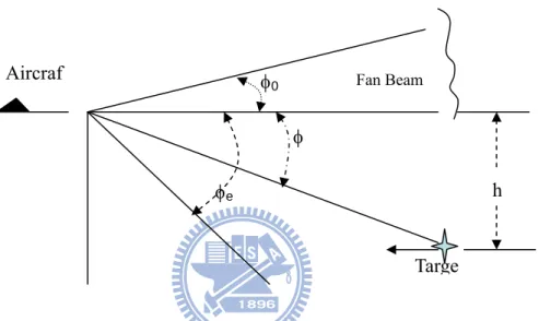
An important property of the cosecant-squared (csc2) antenna is that the target power received from a target at constant altitude, h, remains independent of target range [28]. The cosecant-squared (csc2) antenna pattern of the traditional airborne radar extends the beam coverage of fan-beam antenna where the appended coverage is desired, as shown Fig. 2.8.
Fig. 2.8 Cosecant-squared antenna coverage
The extended coverage is required up to the vertical line passing through the antenna was presented by [28]. In the past, this is impossible with a single antenna to realize csc2 pattern. The csc2 pattern may be generated by a distorted parabolic antenna dish or by proper location of multiple feed horns in a true parabolic antenna.
The gain pattern of a cosecant-squared antenna is given by
1 0 2 2 0 csc csc ) ( ) ( φ φ φ φ φ φ φ =G < < G (2-18) h φ0 φ φe Targe
and signal-to-noise ratio is given by 4 0 4 3 2 ) ( ) 4 ( R R L FkTB R G G P N S n R T TX = = π σ λ (2-19)
the terms of this equation, which depend on the transmitted power PTX, the gains
of transmitted antenna GT and received antenna GR, wavelength of carrier
frequency λ, radar cross section factor σ, distance between radar and target R, noise figure F, the Boltzmann’s constant k (1.38×10⁻²³), noise bandwidth B
n (Hz),
the Kelvin temperature T, and system loss L.
Let GT is equal to GR, Using (2-18) and (2-19) and designating the collection
of constant terms by K, 4 4 csc ) ( R K N S r φ = (2-20)
where the subscript r refers to target return signal-to-noise ratio. From Fig. 2.8, since sinφ = h/R, we get cscφ = R/h where R is the range of the target from the radar. Upon substitution in (2-20)
4 1 ) ( h K N S r = , K1 is constant value (2-21)
which remains constant for constant altitude targets.
Ultimately, the characteristics of the presented antenna array with a csc2θ pattern can compensate for the space loss of 1/R4 that can perform suitably the range measurement of multiple-lane for TMS application.
2.4. System Simulation of FMCW Radar
Then, the previous theoretical result is used and all parameters in the simulation environment (Fig. 2.9) defined. The Advanced Design System (ADS2006) AgilentTM is used to perform the simulation and the behavior model is adopted to construct the FMCW radar system. The behavior models of all the blocks of the above system structure were obtained using each circuit parameter and measurements made in individual IC probe tests. Therefore, the real circuits were not cascaded to the system block and the behavior models applied to construct.
Simulation for External Free Space
Antenna Antenna Attenuator Triangle wave generator IF LO RF Driver
VCO Buffer Power Divider
Isolator LNA Mixer Driver Isolator Isolator R R2 R=50 Ohm Amplifier2 ANT2 VtPulse SRC3 t Amplifier2 ANT1 Attenuator ATTEN3 Amplifier2 AMP1 VCO VCO1 Pad
PAD1 Amplifier2AMP5
IsolatorSML ISO9 PwrSplit2 PWR1 Amplifier2 AMP6 IsolatorSML ISO10 Mixer MIX3 Amplifier2 AMP2 Attenuator ATTEN4 TimeDelay TD1 IsolatorSML ISO11
Fig. 2.9 FMCW radar system simulated environment
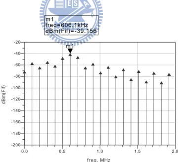
The most important components of the external path in the system simulation were two antennas, a delay line and the attenuators. Gain and return loss information regarding two antennas were obtained by measurement to set antenna blocks; the path loss was derived from the Friis formula, the delay time set based on the phase-delay of the modulated signal, and the RCS of the target
were adjusted, the beat frequencies can be determined and the ranges from the sensor to the target can be also estimated. As presented in Fig. 2.11, an example of beat frequency was derived at a distance of 9 m.
Fig. 2.10 The calculated bandwidth of LFM system is 50 MHz.
Fig. 2.11 The calculated range was set to 9m, and then the derived beat frequency was about 600 KHz. 0.5 1.0 1.5 0.0 2.0 -180 -160 -140 -120 -100 -80 -60 -40 -200 -20 freq, MHz dB m (F if) m1 m1 freq= dBm(Fif)=-39.156606.1kHz 10.45 10.60 -30 -10 -50 10 freq, GHz dB m (f vco ) m10 m11 m10 freq= dBm(fvco)=2.28110.50GHz m11 freq= dBm(fvco)=2.22110.55GHz
CHAPTER 3
Design and Realization of the RF Transceiver
There are two versions of the RF CMOS transceiver in the paper. When the previous version updated to new version, the functions of VCO and more performances of other parts had been improved. And then above two structures of the RF CMOS transceiver have verified by the system simulation.
3.1 First Version CMOS FMCW Chip Design
Figure 3.1 shows the CMOS FMCW RF front-end in the region enclosed by the dashed line. The CMOS single chip transceiver receives an external triangular modulating signal provided by the analog signal-processing unit and feeds the triangular waveform to the on-chip voltage-controlled oscillator (VCO), followed by a buffer amplifier and attenuator. The transmitted signal is then split into two paths. The upper path encounters an isolator followed by a driving amplifier. The lower path encounters an isolator followed by an amplifier driving the local oscillator (LO) input port of the mixer.
Since the power amplifier (PA) needs more consuming power and produces the higher noise level, so the design excluded a PA from the whole RFIC. And the external PA can flexibly adjust the system output power. The RF input port of the mixer receives the signal from the isolator followed by the low-noise amplifier (LNA), which receives the reflected signal from objects. The output of the mixer is fed into the analog signal-processing unit that demodulates received signals.
The CMOS FMCW RF (radio frequency) front-end is depicted in the region enclosed by the dashed line as shown Fig.3.1. The CMOS single chip transceiver receives an external triangular-modulating signal provided by the analog signal processing unit and feed the triangular waveform to the on-chip VCO (voltage-controlled oscillator), followed by a buffer amplifier and an attenuator. Then the transmitted signal is split into two paths. The upper path encounters an isolator followed by a driving amplifier. The lower path encounters an isolator followed by an amplifier driving the LO (local oscillator) input port of the mixer. The mixer’s RF input port receives the signal from the isolator followed by the LNA (low-noise amplifier), which receives the reflected signal from objects. The mixer’s output is fed to the analog signal processing unit for demodulating the received signals. The measurement setup of the probe test described in this section includes a CascadeTM M150 probe station, an AgilentTM 8510C vector network analyzer, an AgilentTM 8565E spectrum analyzer, an AgilentTM 54622A digital oscilloscope, and other accessory cables and tools. Each measured chip was copied from the sub-circuit of the CMOS transceiver in Fig. 3.1 and the measurements were made of sub-circuits of the complete circuit that incorporated I/O pads, which were for probe-testing.
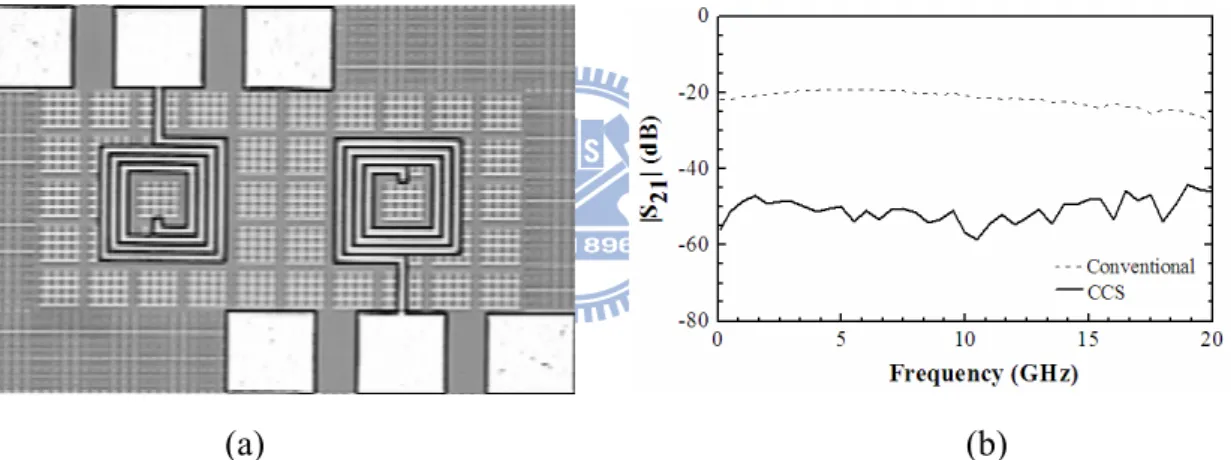
The core technology employed in the CMOS transceiver design is critical to first-pass success of the FMCW sensor. Figure 3.2 shows a photograph of the single chip RF transceiver with each RF building block marked on the chip photo. Chip size is 2.4×1.3 mm, approximately 8.4×10⁻² λ
0 by 4.55×10-2 λ0 at the 10.5-GHz operating frequency. The so-called synthetic quasi-TEM complementary conducting-strip transmission line (CCS-TL) [31], [32] was employed throughout the entire RF chip design.
Fig.3.2 Chip photo of the CMOS FMCW transceiver
The CCS-TL can be identified by closely observing the chip photograph, in which one sees grids distributed throughout the chip. In this chip design, the signal trace is either located on the M6 (top) layer or M5 layer. The meshed ground plane is on the M1 (bottom) layer. The signal portion and perforated ground plane constitute a complementary pair with four arms reaching out for signal interconnections. The main features of the CCS TL are as follows. 1) The CCS TL flexibly synthesizes (non-unique solutions) the characteristic
Power
Divider Isolator
VCO Mixer Isolator LNA
Isolator Driving Amp. Driving Amp. Buffer Amp.
circuit design [32]. 3) The reduction of electromagnetic coupling of adjacent components in the RF CMOS transceiver chip is significant. The CCS TL must be able to densely integrate various RF signal-processing components (Figs. 3.1 and 3.2) into a single chip. When adjacent coupling or crosstalk exist between the transmitting path and receiving path, demodulated signals show interfering signals that resemble an echo from a nearby object. Figure 3.3(a) shows a chip photograph of two closely coupled inductors using CCS TLs [33]. These inductors were placed only 90 μm apart. Figure 3.3(b) shows measured comparative studies of adjacent inductor coupling for inductors made of CCS TLs and inductors integrated directly onto a CMOS substrate.
(a) (b)
Fig. 3.3 (a) The chip photo for measuring cross-coupling of two inductors located 90 μm apart using CCS TLs, and (b) measured transmission coefficient of the adjacent inductors on the CMOS substrate.
Measured results show an approximate 30 dB improvement in coupling reduction at 1 and 20 GHz. Thus, potential CMOS substrate coupling is alleviated by using the synthetic CCS TL. All building blocks and inter-stage connections are utilized by the CCS-TL to achieve the highest attainable isolation required by the FMCW sensor [34]. Notably, the Wilkinson power divider at the upper left corner of the chip photograph (Fig. 3.2), consisting of two 70.7 Ω CCS TLs with a shunt 100 Ω resistor at two output ports, occupies
only 400 μm by 280 μm, occupying 1.372×10⁻⁴λ
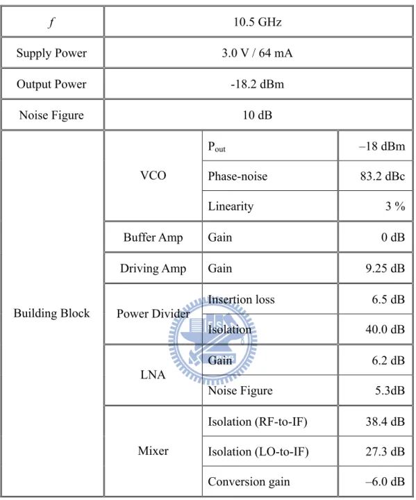
02 in chip area. Measured transmission loss was 6.5 dB, which is very close to the theoretical value of 6.3 dB obtained by the electromagnetic (EM) simulation software of HFSSTM. The measured input (output) reflection coefficient was −16 (−20) dB, which is also very close to theoretical prediction of −15.3 (−22) dB. In [34] the details of how the active building blocks were designed and tested individually in the test chips.
A brief description of the design and test of the CMOS isolator, which is important for providing isolation in the signal path, is given here. The study adopts the circuit topology developed by Podell and Ali [35] and applies it to the 0.18 μm CMOS technology. Figure 3.4 (a) shows the schematics of the CMOS isolator, which is a parallel combination of a common base (M2) and source follower (M1) stage. The capacitor, C1, is used for compensating the insertion loss. The input and output DC blocking capacitors, C2 and C3, are also integrated into the CMOS isolator design. The simple architecture result in the electronic isolator only occupies 300×320 μmofchip area. Figure 3.4(b) shows measurement results of the CMOS isolator. Measurement data implies that the best response of inverse isolation <−25 dB is at 1–20 GHz. Hence, the isolator is added to the transmitter and receiver paths to isolate the VCO from reflecting the signal caused by the impedance mismatch on signal paths.
(a) (b)
Fig. 3.4 (a) Schematics of the CMOS isolator, and (b) measured S-parameters of the 0.18μm CMOS isolator
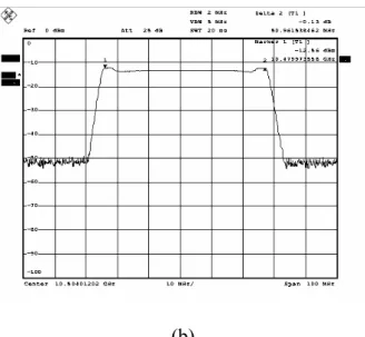
Off-chip package measurement was conducted to evaluate transmitter performance. The continuous-wave (CW) power measured at the output of the external power amplifier was −4.65 dBm, whereas −12.5 dBm was obtained under FMCW modulation with a 50-MHz bandwidth. Figures 3.5 (a) and (b) show the single tone CW output spectrum centered at 10.5 GHz, and the frequency-modulated output spectrum, respectively, illustrating good signal quality ready FMCW sensor assessment.
(a) 1 3 5 7 9 11 13 15 17 19 Frequency(GHz) -35 -30 -25 -20 -15 -10 -5 0 dB S11 S12
(b)
Fig. 3.5(a) The FMCW transceiver at continuous-wave (CW) mode; (b) output spectrum of the FMCW transceiver with frequency modulation at 50.0 MHz
Table 3.1 Performance of Prototype in Fig. 3.2 f =10.5 GHz Gain -2.5 dB Return-loss 10.0 dB Buffer Amp Reverse isolation 8.1 dB Gain 2.2 dB Driving Amp Return-loss -7.0 dB
LNA Noise figure 6.0 dB
Isolation (RF-to-IF) 38.4 dB Isolation (LO-to-IF) 27.3 dB Mixer Conversion gain 3.5 dB Gain -5.0 dB Return-loss 10.1 dB Isolator Isolation 25.2 dB Insertion loss 6.5 dB
Return-loss at input port 16.0 dB
Power Divider
Return-loss at output port 20.2 dB
3.2 New Version CMOS FMCW Chip Design
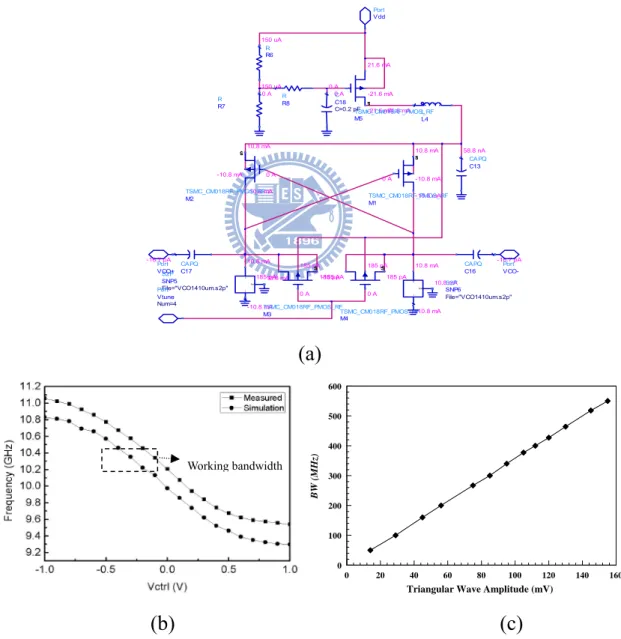
Figure 3.6 shows the building blocks of the X-band FMCW sensor, which are as follows: dual planar antenna arrays at the transmitter output and the receiver input; a 0.18μm 1P6M CMOS fully integrated monolithic transceiver, which performs most of the required RF signal processing, and is shown inside the dashed lines, and a baseband digital signal processing unit for the instantaneous and simultaneous assessment of range measurements. Notably, the use of two antennas rather than only one eliminates the need for a circulator, which is generally expensive and does not provide sufficient isolation between the transmitter and the receiver.
The frequency of the FMCW sensor was set to 10.5GHz to comply with regulations pertaining to transportation management systems for monitoring instantaneous transportation of highway vehicles [14]. The transceiver of the sensor, as enclosed by the dashed line in the Fig. 1.1, was fully implemented by 0.18μm 1P6M CMOS technology. All the components, including voltage controlled oscillator, amplifiers, mixer, power divider, were realized and combined using an innovated guiding structure, called the complementary- conducting-strip transmission line (CCS TL) on the standard silicon substrate. Figure 3.6 shows a photograph of the single-chip CMOS transceiver, containing all necessary RF building blocks of the FMCW sensor system. The chip size, including the necessary contacting pads, was 1.68mm×1.6mm, corresponding to 5.9×10⁻²λ
0 by 5.6×10−2λ0 at 10.5GHz. The pad of the transmitting path in Fig. 3.6 that connects with the TX antenna arrays is enclosed by black lines and labeled “TX”; the other pad of the receiving path in Fig. 3.6 that connects with the RX antenna arrays is also enclosed by black lines and labeled “RX”.
The guiding technology adopted in the design of CMOS FMCW transceiver is essential to the first-pass success of the sensor system. The CCS TL was adopted throughout the RF chip design, [31]-[32]. The proposed chip locates the signal trace on the top metal layer, and the meshed ground plane on the bottom metal layer [36]. The CCS TL significantly reduces the electromagnetic coupling of the adjacent components on the CMOS substrate, where various RF transceiver building blocks must be compact and placed in close proximity to save chip area [34],[36]. Hence, all building blocks and their inter-stage connections are realized by the CCS TLs in order to maximize the attainable isolation required by the FMCW sensor. The good isolation achieved in the CMOS RF transceiver diminishes the degree of difficulty of the IF filter design or DSP control method, thus canceling the leakage from the transmitting port to the receiving port [37].
Fig.3.6 The 0.18μm CMOS FMCW transceiver. The chip comprises a VCO, a buffer amplifier, a power divider, a low-noise amplifier and two driving amplifiers.
VCO Mixer RX LNA
Power Divider Amp_LO Amp_TX
Fig. 1.1. The transmitted signal is then split into two paths using an integrated two-way equal-split power divider, which is fully realized by the CCS TL. Figure 3.6 shows the two-way Wilkinson power divider, which is located on the upper left corner of the chip, and which comprises two 70.7Ω CCS TLs and an isolation resistor of 100Ω shunting two output ports. The size of the power divider is only 400μm×280μm, corresponding to 1.372×10⁻⁴λ
02 at 10.5GHz. The driving amplifier (Amp_TX in Fig.3.6) is fed by the upper output of the power divider through a CCS TL with a length of 320µm, thus completing the transmitter path of the CMOS transceiver. The lower output port is connected to another driving amplifier (Amp_LO in Fig.3.6) by a CCS TL of 670µm. The two driving amplifiers are identical in the present CMOS transceiver. Figure 3.7 shows the measured results of a composite network comprising two driving amplifiers and a CCS TL power divider. The network had transmission coefficients of −2.0dB and 0dB for the TX-path and the LO-path, respectively. The measured input reflection coefficient at 10.5GHz was about −16.6dB in the 50Ω system. The measured isolation between the TX-port and the LO-port at 8–12GHz was higher than 40dB, revealing that the network combining the CMOS Wilkinson power divider and driving amplifier had very low electromagnetic coupling. The design of the voltage control oscillator is based on the typical differential cross-coupled VCO, which is well documented [38]. The p-type differential cross-coupled pair is considered as a negative differential resistor, and the core resonator is realized by two quarter-wavelength CCS TLs (Fig. 7 of [39]). To simplify the thesis and because of the special purpose to which is applied, the measurement of speed is omitted. The measured chip is copied from the sub-circuit of the CMOS transceiver in Fig. 3.6 which comprising two driving amplifiers and a CCS TL power divider. The measured
frequencies are from 8 to 12GHz and the measured scatter parameters of the on-chip are shown in Fig. 3.7. The measurements were made of sub-circuits of the complete circuit that incorporated I/O pads, which were for probe-testing.
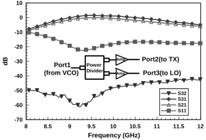
8 8.5 9 9.5 10 10.5 11 11.5 12 Frequency (GHz) -70 -60 -50 -40 -30 -20 -10 0 10 dB S32 S31 S21 S11 Port1 (from VCO) Port2(to TX) Port3(to LO) Power Divider Amp Amp
Fig. 3.7 Measured scatter parameters of the on-chip TL-based power divider with two driving amplifiers in the 50Ω system.
The MOS capacitor is applied as a varactor for the frequency control of the VCO shown in Fig. 3.8(a). According to the on-chip measurements, the output power of the VCO was −18dBm, and its corresponding phase noise was −83.2dBc with an offset frequency of 100.0 KHz from the carrier at 10.5GHz. Figure 3.8(b) illustrates the frequency tuning at 9.3GHz–11.0GHz. The fundamental linearity that enclosed by the dashed line in Fig. 3.8(b) was about 0.06%. However, the VCO linearity cannot immediately be applied to estimate the performance of the FMCW system. The real linearity of VCO corresponds to the definition of linearity of FMCW system, since the range resolution correlates directly with the modulated bandwidth. Therefore, a new method is adopted to calculate the linearity of VCO. Additionally, the proposed VCO is experimentally characterized with the input triangular wave. Figure 3.8(c) shows
peak value of the triangular wave. Increasing the amplitude of the control voltage from 12.0mV to 150.0mV increased in the bandwidth of the output frequency-modulated signal from 50.0MHz to 550.0MHz. The VCO linearity under a modulation bandwidth of 500MHz was estimated as 3.0 % by following the computation in Fig. 6 [39]. The curve shown in Fig. 3.8(c), based on (2-4) in chapter 2, is directly linked to the control-scheme for the range measurement using the proposed CMOS sensor in the chapter.
-10.8 mA 10.8 mA 10.8 mAS2P SNP6 File="VCO1410um.s2p" 2 1 Ref -10.8 mA 10.8 mA 10.8 mA S2P SNP5 File="VCO1410um.s2p" 2 1 Ref Port Vtune Num=4 Port Vdd -21.6 mA L L4 21.6 mA -21.6 mA -21.6 mA 0 A TSMC_CM018RF_PMOS_RF M5 150 uA R R6 0 A R R8 150 uA R R7 -16.7 pA CAPQ C16 58.8 nA CAPQ C13 -10.8 mA 10.8 mA -10.8 mA 0 A TSMC_CM018RF_PMOS_RF M1 -10.8 mA 10.8 mA -10.8 mA 0 A TSMC_CM018RF_PMOS_RF M2 -185 pA 185 pA 185 pA 0 A TSMC_CM018RF_PMOS_RF M4 -185 pA 185 pA 185 pA 0 A TSMC_CM018RF_PMOS_RF M3 Port VCO-Port VCO+ -16.7 pA CAPQ C17 0 A C C18 C=0.2 pF (a) 0 20 40 60 80 100 120 140 160
Triangular Wave Amplitude (mV)
0 100 200 300 400 500 600 BW (M Hz) (b) (c)
Fig. 3.8 (a) Schematic of the VCO by the MOS capacitor, (b) Frequency tuning characteristics, and (c) measured modulated bandwidth against the input amplitude, of the triangular wave for the on-chip VCO in CMOS transceiver.
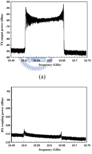
The receiver path comprises a mixer and an LNA. The mixer was a MICROMIXER, as described by B. Gilbert [40]. The single-ended RF input was matched and converted differentially to the core of the mixer. The output of the IF was located on the left-hand side of the CMOS transceiver, followed by the external digital signal processing unit for the signal analyses. The measured LO-port reflection coefficient, RF-port reflection coefficient and conversion gain of the mixer were −12dB, −17dB and −6 dB, respectively. The isolations between the adjacent ports of the mixer were characterized by the on-wafer measurements. Furthermore, the isolations between the transmitting path and receiving path in the proposed transceiver were also experimentally studied [33], [36]. The on-chip VCO was activated and controlled by the triangular wave during the experiments. An AgilentTM 8565E spectrum analyzer was adopted to observe the signal at output and input ports of the transmitting and receiving paths, respectively. Figures 3.9(a) and (b) display two measured spectrums. The power spectrum of the receiving path was 55dB less than that of the transmitting path at 10.5GHz. These measured results confirm that the proposed system obtained high leakage suppressions by using the CCS TL guiding structure throughout the entire chip design. Since the original power spectrum of receiving path in Fig. 3.9(b) was sunk in the noise floor by the general parameters setting of the spectrum analyzer, the slight power of receiving path wasn’t discovered until the resolution bandwidth (RBW) of the spectrum analyzer was properly adjusted. To ensure consistency of measurement, to RBW of the spectrum analyzer is set to the same value in the measurement of