適用於共電流雙頻帶接收機前端電路之偶次諧波混頻器設計
70
0
0
全文
(2) 適用於共電流雙頻帶接收機前端電路 之偶次諧波混頻器設計 Design of Sub-Harmonic Mixer For Concurrent Dual-Band Receiver Front-End. 研究生:吳俊賢. Student:Chun-Hsien Wu. 指導教授:周復芳 博士. Advisor:Dr. Christina F. Jou. 國立交通大學 電信工程學系碩士班 碩 士 論 文 A Thesis Submitted to Department of Communication engineering College of Electrical Engineering and Computer Science National Chiao Tung University In Partial Fulfillment of the Requirements For the Degree of Master of Science In Communication Engineering June 2005 Hsin Chu, Taiwan, Republic of China. 中 華 民 國 九 十 四 年 六 月.
(3) 適用於共電流雙頻帶接收機前端電路之偶次諧波混頻器設計 . 研究生:吳俊賢 . . 指導教授:周復芳 博士 . 國立交通大學電信工程學系碩士班 . 摘要 由於吉爾伯混頻器在直接降頻或低中頻接收機的應用中,存在著本地振盪訊 號洩漏的問題,這將會導致中頻輸出端產生直流偏差而破壞接收機的特性。因 此,在本論文中首先提出一個雙平衡式偶次諧波混頻器,它的動作原理是以吉爾 伯混頻器為基礎。此一混頻器的特點是,所需的本地振盪訊號頻率是射頻訊號頻 率的一半,故改善了直流偏差的問題。 接著我們將此偶次諧波混頻器應用到接收機中,藉由它的二倍頻特點,我們 提出一個應用於 802.11a/b/g 的全新共電流雙頻帶接收機架構,而這個新的雙頻 帶接收機架構僅需一組本地振盪源。在第三章中,我們整合了共電流雙頻帶低雜 訊放大器及偶次諧波混頻器來實現共電流雙頻帶接收機前端電路。 以上兩組晶片皆以 CMOS 0.18µm 的製程實現,除了電路的描述及模擬結果 外,實際量測結果也涵括在這篇論文之中。如同一般射頻工程師所可能遇到的困 難,量測結果與實驗結果並不完全相符,因此我們也分別對兩者之間的差異以及 可能的原因作一些說明和探討。 . I.
(4) Design of Sub-Harmonic Mixer For Concurrent Dual-Band Receiver Front-End Student:Chun-Hsien Wu. Advisor:Dr. Christina F. Jou. Department of Communication engineering College of Electrical Engineering and Computer Science National Chiao Tung University Abstract Since Gilbert mixer has the problem of the LO leakage in the direct conversion or low-IF receiver applications, this will cause the DC offset in the IF output port to degrade the performance of the receiver. In this thesis, we completed a double-balanced sub-harmonic mixer with its design approach based on the classical Gilbert mixer. This mixer with an LO signal operating at half of RF frequency can improve the DC offset in the IF output port. Then we apply this sub-harmonic mixer to the receiver. By employing this sub-harmonic mixer with an LO signal operating at half of RF frequency, we propose a new concurrent dual-band receiver architecture with only one frequency synthesizer for 802.11a/b/g applications in this thesis. We integrate the concurrent dual-band LNA and sub-harmonic mixer to implement the concurrent dual-band receiver front-end in Chapter 3. These two IC have fabricated in a CMOS 0.18µm technology. Except the circuit descriptions and simulated results, this thesis includes the measured results of the circuits mentioned earlier. As all designers may be confronted with, the measurement results fall short of simulation results. Thus, we also discuss the differences between simulations and measurements and the possible reasons. II.
(5) 誌 謝 進入實驗室這兩年來,在射頻電路的領域上,從懵懂無知到略有心得,這一 切都要感謝指導教授周復芳老師的悉心指導,並提供一個良好的研究環境,讓學 生能順利完成碩士學位。以及國華學長亦師亦友的給予實驗室同學最大的協助, 讓我們能得到最豐富的學習資源及科技資訊。 接著要感謝在 919 實驗室和我一起打拼兩年的同學們,偉誠、家良、柏達、 欽賢及政宏,感謝你們平時的包容與鼓勵,讓我克服了許多生活及研究中的小低 潮。雖然大家終究要往人生不同的目標邁進了,我相信我們都會在世界的不同角 落祝福著對方。已畢業的盈蒼、炳宏、政良及汪揚學長,常在困惑時提供自己的 寶貴經驗供我參考,讓我順利解決所碰到的問題。碩一的小砲、小明、小秋、小 賴、仕豪及博揚學弟,還有專題生 sammy 及小郭學弟,感謝你們在碩士生涯的陪 伴,有你們的協助,分擔了我在研究之餘所無法空出時間處理的瑣事,祝福你們 在往後的日子也都能達到自己的期望順利畢業。謝謝大家在研究及生活上的協助 與關照,有了大家的陪伴,使得平淡的研究生活多了不少樂趣,這兩年的生活因 為你們而顯得多采多姿,讓我擁有了許許多多美好的回憶。 另外要感謝南工的兩位啓蒙老師,張瑞娟老師及陳芸華老師,有您們的教 導,學生才能在求學生涯中走得平穩且完成學業,由衷的感謝您們。一路陪伴著 我走來的好友們,更是在這過程中扮演著不可或缺的角色,謝謝大家。 最後,感謝父母及家人對我的鼓勵,讓我有一個穩定的環境能專心致力於發 展,這股安定的力量是我前進的原動力。僅以此論文獻給所有關心我的人,希望 你們能感受到我由衷的謝意。 俊賢 2005 夏 新竹 風城. III.
(6) CONTENTS CHINESE ABSTRACT.......................................................................... I ENGLISH ABSTRACT........................................................................ II ACKNOWLEDGMENT .....................................................................III CONTENTS.......................................................................................... IV TABLE CAPTIONS............................................................................. VI FIGURE CAPTIONS .........................................................................VII. Chapter 1. INTRODUCTION .............................................................1. 1.1. Background and Motivations.....................................................................1. 1.2. Thesis organization ....................................................................................4. Chapter 2 SUB-HARMONIC MIXER USING 0.18µm CMOS......6 2.1. 2.2. Mixer Fundamental....................................................................................6 2.1.1. Principles of Frequency Translation .................................................6. 2.1.2. Topology ...........................................................................................7. 2.1.3. Effects of Nonlinearity....................................................................11. 2.1.4. Conversion Gain .............................................................................12. 2.1.5. Intermodulation...............................................................................13. 2.1.6. Noise ...............................................................................................15. 2.1.7. Port Return Loss .............................................................................16. 2.1.8. Port Isolation...................................................................................17. Design of Sub-Harmonic Mixer...............................................................17 2.2.1. Architecture and Circuit Design .....................................................17. 2.2.2. Design Flow ....................................................................................21 IV.
(7) 2.2.3 2.3. 2.4. Circuit Layout .................................................................................22. Measurement of Sub-Harmonic Mixer ....................................................24 2.3.1. Measurement Consideration ...........................................................24. 2.3.2. Measurement Results ......................................................................29. Comparison ..............................................................................................33. Chapter 3. CONCURRENT DUAL-BAND RECEIVER FRONT-END USING 0.18µm CMOS...........................36. 3.1. 3.2. 3.3. 3.4. Review of Receiver Architecture .............................................................36 3.1.1. Superheterodyne Receiver ..............................................................36. 3.1.2. Direct Conversion Receiver............................................................38. 3.1.3. Low-IF Receiver .............................................................................39. Design of Concurrent Dual-Band Receiver .............................................39 3.2.1. Architecture.....................................................................................40. 3.2.2. Circuit Implementation ...................................................................42. 3.2.3. Circuit Layout .................................................................................45. Measurement of Concurrent Dual-Band Receiver...................................46 3.3.1. Measurement Consideration ...........................................................46. 3.3.2. Measurement Results ......................................................................48. Comparison ..............................................................................................51. Chapter 4. CONCLUSIONS AND FUTURE PROSPECTS ..........53. 4.1. Conclusions..............................................................................................53. 4.2. Future Prospects.......................................................................................54. REFERENCES......................................................................................56. V.
(8) TABLE CAPTIONS Table 2.1. Performance Summaries of the sub-harmonic mixer............................34. Table 2.2. Comparison of sub-harmonic mixer .....................................................35. Table 3.1. Performance summaries of the dual-band receiver front-end...............51. Table 3.2. Comparison of dual-band receiver front-end........................................52. VI.
(9) FIGURE CAPTIONS Fig. 1.1. Simple direct conversion receiver..............................................................2. Fig. 1.2. DC offset mechanisms in the direct conversion receiver...........................2. Fig. 1.3. Improved DC offset mechanisms built by sub-harmonic mixer ................3. Fig. 2.1. (a) Single-balanced mixer (b) Double-balanced mixer..............................7. Fig. 2.2. Optimum LO power considering (a) conversion gain (b) noise figure....10. Fig. 2.3. Differential pair with (a) constant current source (b) grounded source...11. Fig. 2.4. Nonlinear model of transconductor stage in single-balanced mixer........14. Fig. 2.5. (a) Double-balanced sub-harmonic mixer (b) Common-drain output buffer (c) Off-chip matching network of the LO port ........................................20. Fig. 2.6. Operation of double LO frequency ..........................................................20. Fig. 2.7. Design flow of the sub-harmonic mixer ..................................................22. Fig. 2.8. Layout of the double-balanced sub-harmonic mixer ...............................24. Fig. 2.9. Structure of the shielded signal PAD .......................................................24. Fig. 2.10 Photograph of the (a) RF port rat-race (b) LO port rat-race (c) LO port quadrature hybrid .....................................................................................25 Fig. 2.11 Photograph of the LO port quadrature Balun ..........................................26 Fig. 2.12 PCB test board layout of the sub-harmonic mixer...................................27 Fig. 2.13 Practical PCB test board of the sub-harmonic mixer...............................28 Fig. 2.14 Die photograph of the double-balanced sub-harmonic mixer..................28 Fig. 2.15 Measurement setup for (a) conversion gain (b) input return loss testing (c) two-tone IIP3 testing................................................................................29 Fig. 2.16 Current of the mixer core for transistor M1 .............................................30 Fig. 2.17 Current of the output buffer .....................................................................30 VII.
(10) Fig. 2.18 RF port return loss of the sub-harmonic mixer........................................31 Fig. 2.19 LO port return loss of the sub-harmonic mixer .......................................32 Fig. 2.20 Conversion power gain of the sub-harmonic mixer.................................32 Fig. 2.21 1dB compression point of the sub-harmonic mixer.................................32 Fig. 2.22 Third-order-interception point of the sub-harmonic mixer......................33 Fig. 2.23 Measured IF output waveform of the sub-harmonic mixer .....................33 Fig. 3.1. Superheterodyne receiver.........................................................................37. Fig. 3.2. Direct conversion receiver .......................................................................38. Fig. 3.3. Low-IF receiver .......................................................................................39. Fig. 3.4. Conventional architecture of a dual-band receiver ..................................41. Fig. 3.5. Proposed architecture of the concurrent dual-band receiver....................41. Fig. 3.6. Receiving band distribution of WLAN in the range of 2.4~6 GHz.........42. Fig. 3.7. Frequency plan of the concurrent dual-band receiver..............................42. Fig. 3.8. Single-ended dual-band LNA ..................................................................43. Fig. 3.9. Sub-harmonic mixer for 5.25 GHz band..................................................44. Fig. 3.10 Gilbert mixer for 2.45 GHz band.............................................................45 Fig. 3.11 (a) Layout of the concurrent dual-band receiver front-end (b) Die photo of the concurrent dual-band receiver front-end............................................46 Fig. 3.12 PCB test board layout of concurrent dual-band receiver front-end for (a) 2.45 GHz band (b) 5.25 GHz band ..........................................................47 Fig. 3.13 Practical PCB test board of concurrent dual-band receiver front-end for (a) 2.45 GHz band (b) 5.25 GHz band ..........................................................47 Fig. 3.14 Measurement setup of concurrent dual-band receiver front-end .............48 Fig. 3.15 RF port return loss of the receiver front-end ...........................................49 Fig. 3.16 LO port return loss of the receiver front-end for (a) 802.11b/g band (b) 802.11a band ............................................................................................49 VIII.
(11) Fig. 3.17 1-dB compression point of the receiver front-end for (a) 802.11b/g band (b) 802.11a band ............................................................................................50 Fig. 3.18 Third-order-interception point of the receiver front-end for (a) 802.11b/g band (b) 802.11a band..............................................................................50 Fig. 3.19 Measured IF output waveform of the receiver front-end for (a) 802.11b/g band (b) 802.11a band..............................................................................50. IX.
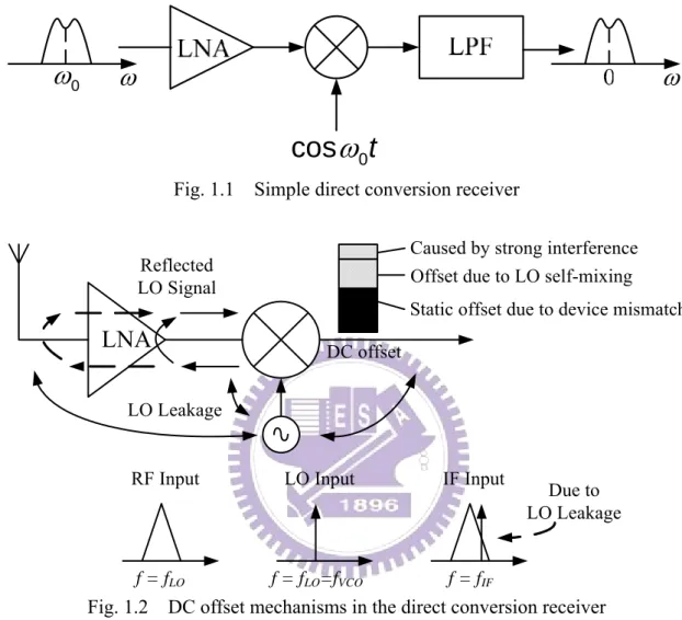
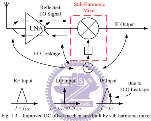
(12) Chapter 1 INTRODUCTION 1.1 Background and Motivations A low power RF device becomes a tendency as applied in the portable wireless communication systems. However, the performance including linearity and conversion gain will be degraded when we reduce the power or the supply voltage of the RF mixer circuit. Hence, the implementation of the mixer with low power consumption, high linearity, and high conversion gain would be a challenge in the RF front-end circuit.. Shown in Fig. 1.1 is a simple direct conversion receiver, where the LO frequency is equal to the input carrier frequency. It has been attracting attention as a possible architecture for realizing a single-chip receiver. However it has two serious problems that need to be overcome. One is dc offset caused by self-mixing of the local oscillator (LO) signal and the other is second-order intermodulation (IM2). The dc offset problem is shown in Fig. 1.2, where the one path is the LO frequency bypassed to the output; another path, where the LO leakage reflected from the antenna is amplified by the LNA. In addition, the LO signal not only directly enters the mixer but also couples into the mixer through parasitic capacitors. This amplified LO leakage and the coupled LO signal will be injected together into the input port of the. 1.
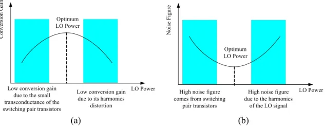
(13) mixer and down-converted to IF. Therefore, these coupling behaviors will reduce the dynamic range of the IF signal.. ω0. ω. ω. cos ω0t Fig. 1.1. Simple direct conversion receiver Caused by strong interference Offset due to LO self-mixing. Reflected LO Signal. Static offset due to device mismatch. LNA. DC offset. LO Leakage. RF Input. LO Input. IF Input. f = fLO. f = fLO=fVCO. f = fIF. Fig. 1.2. Due to LO Leakage. DC offset mechanisms in the direct conversion receiver. The presence of dc offset “noise” at the IF baseband due to LO self-mixing, therefore, not only reduces the signal-to-noise ratio (SNR) of the direct conversion receiver while the desired down-converted signal is also at or near dc; but also reduces the linearity of the direct conversion receiver because of the reduced dynamic range of the IF signal. To improve the dc offset problem, we adopt the active sub-harmonic mixer as shown in Fig. 1.3. The dc offset variation due to the self-mixing can be reduced down to its noise level with this sub-harmonic mixer. In Fig. 1.3, the RF signal is mixed with the second harmonic of LO signal and modulated. 2.
(14) as the desired output frequency ( f IF = f RF − 2 f LO ), where f IF , f RF , and f LO are the IF, RF, and LO frequencies, respectively. In addition, the LO frequency provided by the local oscillators can be lower than the general mechanism and relax the local oscillator design.. Fig. 1.3 Improved DC offset mechanisms built by sub-harmonic mixer Since 1999, the WLAN market has experienced tremendous growth [1] [2]. By the rapid development and large demand of wireless communication, the fully integrated monolithic multi-band radio transceivers are the most significant considerations for communication applications. Wireless LANs provide wideband wireless connectivity between PCs and other consumer electronic devices, allowing access to core networks and other equipment in office and home environments.. Growing market demands of low cost for present WLAN systems push system architecture from multiple-path-multiple-band to concurrent multiple-band type. Using conventional receiver architectures, simultaneous operation at different 3.
(15) frequencies can only be achieved by building multiple independent signal paths with an inevitable increase in the cost, chip area and power dissipation [3]~[7]. A concurrent dual-band receiver architecture is introduced to be capable of simultaneous operation at two-different frequencies without dissipating twice as much power or a significant increase in cost and chip area [8] [9]. The principal challenge in this concurrent dual-band receiver arises from the tuning range of frequency synthesizer because of the usage of two Gilbert mixers. In other words, this topology needs two LO signals with large frequency difference. Considering the tuning range of on-chip voltage-controlled oscillator, the only possible solution for the topology may be implementing two frequency synthesizers. By employing a sub-harmonic mixer with an LO signal operating at half of RF frequency, a new concurrent dual-band receiver architecture with only one frequency synthesizer for 802.11a/b/g applications is proposed in this thesis. The common properties suggest that the two standards can be accommodated in this concurrent dual-band receiver while sharing some of the components. A concurrent dual-band receiver front-end consisting of a differential concurrent dual-band LNA, a Gilbert mixer, and a sub-harmonic mixer is designed and implemented in this thesis. This low power front-end takes 16 mA from a 1.8-V supply.. 1.2 Thesis organization This thesis discusses about the front-end circuits design and implementation for WLAN frequency band. The contents consist of two major topics: “A 0.18µm CMOS 5.25 GHz sub-harmonic mixer” and “A 0.18µm CMOS concurrent dual-band receiver front-end”, respectively in Chapter 2 and Chapter 3. We will present the design flow and experimental results. Here is the organization of this thesis.. 4.
(16) In Chapter 2, we present the design and implementation of a sub-harmonic mixer. Here we introduce the fundamental and design flow of the mixer. We will also illustrate the consideration for PCB measurement.. In Chapter 3, a concurrent dual-band receiver front-end consisting of a differential concurrent dual-band LNA, a Gilbert mixer, and a sub-harmonic mixer is designed and implemented. The simulation and measurement results comparison is in section 3.3.. In Chapter 4, we make the conclusion and then present the future prospects.. 5.
(17) Chapter 2 SUB-HARMONIC MIXER USING 0.18µm CMOS. Mixer is a key building block in a communication system that performs frequency translation for down-conversion or up-conversion. Modern wireless communication systems demand stringent dynamic range requirements. The dynamic range of a receiver is often limited by the first downconversion mixer. This forces many compromises between figures of merit such as conversion gain, linearity, dynamic range, noise figure and port to port isolation of the mixer. Integrated mixers become more desirable than discrete ones for higher system integration with cost and space savings. In order to optimize the overall system performance, there exist a need to examine the merits and shortcomings of each mixer feasible for integrated solutions. In Chapter 2, we introduce the basics of mixers and some indices to evaluate a mixer.. 2.1 Mixer Fundamental 2.1.1 Principles of Frequency Translation The basic idea to generate an output frequency component that is absent from the input port is to multiply two signal of different frequencies. It can be expressed as. 6.
(18) ( A cos ωRF t )( B cos ωLOt ) =. AB ⎡cos (ωRF + ωLO ) t + cos (ωRF − ωLO ) t ⎤⎦ 2 ⎣. (2.1). From the above equation, the multiplication of two signals at the frequency. ωRF and ωLO produce signals at the frequency (ωRF + ωLO ) and (ωRF − ωLO ) . Therefore, we can obtain the up-converted and down-converted ωRF ± ωLO frequencies.. 2.1.2 Topology Generally speaking, the mixer can be basically categorized as single-balanced and double-balanced types.. (a) (b) Fig. 2.1 (a) Single-balanced mixer (b) Double-balanced mixer Fig. 2.1(a) shows a single-balanced mixer which accommodates a differential LO signal and a single-ended RF signal. The single-balanced mixer can eliminate effectively feedthrough of the RF signal to the IF signal, which can lead to finite even-order distortion. But the mixer has a main disadvantage that is the LO-IF feedthrough. If the IF frequency is lower than LO, the LO signal can be filtered out by IF filter easily. Fig. 2.1(b) shows a double-balanced mixer that operates with both differential RF and LO inputs. This mixer has several interesting features such as high 7.
(19) conversion gain, low LO power, good isolation, and monolithic integration capability. Due to these attractive features of the double-balanced mixer, this mixer is most popular topology of active mixer in RF applications. A. Single-Balanced Mixer The single-balanced mixer offers a desired single-ended RF input for ease of application. The mixer comprises a common-source stage (M1) and a differential switching quad (M2 and M3). In Fig. 2.1(a), we assume that the mixer under large LO driver and the mixer commutates the RF transconductance current with a square wave. Referring to Fig. 2.1(a), suppose a unit sinusoidal input voltage of frequency ωRF is linearity converted to a current, and commutated by the switched at ωLO , which amounts to multiplying the sinusoidal current by a square wave, sq (ωLO t ) , alternating between +1 and -1. Then the differential current of RL loads is I IF = g m1VRF sin ωRF t × sq (ωLO t ). 1 ⎛ 4 ⎞⎛ ⎞ = g m1VRF sin ωRF t × ⎜ ⎟⎜ sin ωLO t + sin 3ωLO t + " ⎟ 3 ⎝ π ⎠⎝ ⎠ ⎛2⎞ = ⎜ ⎟ g m1VRF ⎡⎣cos (ωRF − ωLO ) t + cos (ωRF + ωLO ) t ⎤⎦ + " ⎝π ⎠. (2.2). where gm1 is the transconductance of M1.. If low-side mixing (LO frequency is lower than RF frequency) is used, ( ωRF − ωLO ) and ( ωRF + ωLO ) terms are the wanted and unwanted signals, respectively. Eq. (2.2) shows a current conversion loss of at least. 2. π. Consequently, the conversion gain therefore can be obtained as 8. through this mixer..
(20) Conversion Gain =. 2. π. g m1 RL. (2.3). Now, if we consider the switching time of transistors M2 and M3, we can re-express Eq. (2.3) as. Conversion Gain ≈. ⎛ ⎞ 2 (Vgs − Vt ) M 2, M 3 ⎟ g m1 RL ⎜1 − ⎜ ⎟ π π VLO ⎝ ⎠ 2. (2.4). where VLO is the amplitude of the LO signal [10].. In Eq. (2.4), we can choose the size of M1 and the load resistance RL according to the desired conversion gain. Choosing RL, we must tread off the linearity and the conversion gain of the mixer.. The switching quad should be driven by a large LO signal to minimize its noise contribution when all transistors (M2 and M3) are active. The reason is that larger LO voltage swing is needed to turn off one side of the FET switching quad. Besides, linearity, and power consumption considerations set the upper limit on the LO amplitude. A very large LO amplitude results in excessive current being pumped into the source edges of the switching quad through the gate-source capacitance and thus generates additional IM3. Larger LO amplitudes also decrease the voltage headroom at the mixer output. Another disadvantage of using large LO amplitude is the increased power consumption. In brief, is shown in Fig. 2.2, the choice of the LO amplitudes is very important to the mixer design. There exist different optimum LO powers for the conversion gain and noise figure. Through simple in design, it can achieve a moderate gain and low noise figure. However, the design has low P1dB, low port to port isolation, and low IIP3. 9.
(21) Noise Figure. Conversion Gain. Optimum LO Power. Optimum LO Power. Low conversion gain due to the small transconductance of the switching pair transistors. Low conversion gain due to its harmonics distortion. LO Power. High noise figure comes from switching pair transistors. High noise figure due to the harmonics of the LO signal. LO Power. (a) (b) Fig. 2.2 Optimum LO power considering (a) conversion gain (b) noise figure B. Double-Balanced Mixer Fig. 2.1(b) shows the basic circuit topology of a double-balanced or Gilbert-type mixer. The mixer is consisting of a differential-pair driver stage (M1 and M2) and a differential switching quad (M3~M6). It is important that M1 and M2 and M3~M6 are matched, respectively, for the symmetric purpose. The Gilbert-type mixer is desirable for high port to port isolation and spurious output rejection applications. It can provide high gain and very low noise figure, and the linearity is reasonably good. In addition, it has the advantage of rejecting the strong local oscillator (LO) component and the even-order distortion products.. The sources of the differential pair for the RF inputs are connected to ground. It is found that a differential pair with a constant current source shown in Fig. 2.3(a) generates higher IM3, than that of a grounded source pair shown in Fig. 2.3(b) biased at the same current. This can be explained by writing down their differential current equations as follows [11].. 10.
(22) +. M1. M2. M1. +. Vin -. M2. Vin ISS. (a) (b) Fig. 2.3 Differential pair with (a) constant current source (b) grounded source In Fig. 2.3(a):. I out = I D1 − I D 2 =. 1 W µnCox Vin 2 L. 2 I ss. − Vin 2. (2.5). 1 W µnCox Vin (Vgs1 + Vgs 2 − 2Vth ) 2 L. (2.6). 1 µC W 2 n ox L. In Fig. 2.3(b):. I out = I D1 − I D 2 =. According to Eq. (2.6), Iout depends linearity on Vin and the bias Vgs1 + Vgs2-2Vth sets the transconductance, so there are no IM3 products in the output of the grounded sources differential pair. However, the short-channel effects, such as nonlinear channel-length modulation and the mobility descending with vertical field, may also yield IM3 in reality.. 2.1.3 Effects of Nonlinearity While many analog and RF circuits can be approximated with a linear model to obtain their response to small signals, nonlinearities often lead to interesting and. 11.
(23) important phenomena. For simplicity, we limit our analysis to memoryless, time-variant systems and assume y ( t ) ≈ α1 x ( t ) + α 2 x 2 ( t ) + α 3 x 3 ( t ). (2.7). If a sinusoid is applied to a nonlinear system, the output generally exhibits frequency components that are integer multiples of the input frequency. In Eq. (2.7), if x ( t ) = A cos ωt , then y ( t ) = α1 A cos ωt + α 2 A2 cos 2 ωt + α 3 A3 cos3 ωt. = α1 A cos ωt +. =. α 2 A2 ⎛ 2. α 2 A2. + ⎜ α1 A + ⎝. 2. (1 + cos 2ωt ) +. α 3 A3 4. ( 3cos ωt + cos 3ωt ). 3α 3 A3 ⎞ α 3 A3 α 2 A2 t + t + ω ω cos cos 2 cos 3ωt ⎟ 4 ⎠ 2 4. (2.8). In Eq. (2.8), the term with the input frequency is called the “fundamental” and the higher-order terms the “harmonics.”. From the above expansion, we can make two observations. First, even-order harmonics result from α j with even j and vanish if the system has odd symmetry, i.e., if it is fully differential. In reality, however, mismatches corrupt the symmetry, yielding finite even-order harmonics. Second, in Eq. (2.8) the amplitude of the nth harmonic consists of a term proportional to An and other terms proportional to higher powers of A.. 2.1.4 Conversion Gain A downconversion mixer should provide sufficient power gain to compensate for 12.
(24) the IF filter loss, and to reduce the noise contribution from the IF stages. However, this gain should not be too large as a strong signal may saturate the output of the mixer. Typically, power gain, instead of voltage or current gains, is specified. The reason is that noise figure is a power quantity, and hence it is easier to translate the NF of the IF stages to the system NF using power gain. Power gain (G) is related to voltage or current gain by 2. 2. ⎛V ⎞ R ⎛ I ⎞ R G =⎜ O ⎟ S =⎜ O ⎟ L ⎝ VI ⎠ RL ⎝ I I ⎠ RS. (2.9). where VO and VI are output and input voltages, respectively; I O and I I are output and input currents, respectively; RL and RS are load and source resistance, respectively. Although increasing the load resistance by a factor of 2 can increase the voltage gain by 6 dB, the power gain is increased by only 3 dB.. 2.1.5 Intermodulation For nonlinear circuits such as mixer having multiple non-commensurate small-signal excitations, the nonlinearities in these circuits are often so weak that they have a negligible effect on their linear responses. In view of these references, the 1dB compression point can be computed by taking the ratio of all harmonic terms to it linear term and setting the ratio equal to -1dB (0.891). The IIP3 can be computed by equating the amplitude of the third-order intermodulation products terms with linear term [12]. Fig. 2.4 shows the nonlinear model of the transconductor stage to derive the nonlinearity equations for the single-balanced mixer.. 13.
(25) Fig. 2.4 Nonlinear model of transconductor stage in single-balanced mixer Using the model in Fig. 2.4, Kirchhoff’s voltage law yields:. Vs = ( Z g + Rg )( I gs + I gd ) + Vgs + Z s ( I gs + g mVgs I ds ). where I ds =. g ds ( sC gdVgs + I d − g mVgs ) g ds + sCgs. , I gd = g mVgs − I d +. (2.10). g ds ( sC gdVgs + I d − g mVgs ) g ds + sCgs. Using this relationship and Volterra series expression of Id, the Volterra series coefficients are decided. From the Volterra series coefficients, the magnitude of output signal component at frequency 2ω2 − ω1 or 2ω1 − ω2 determine the input-referred third-order intermodulation product (IM3) which also depends on. 1 + jωC gs ⎡⎣ Z s (ω1 , Ls ) + Z g (ω1 , Ls ) ⎤⎦. (2.11). Where the inductive degeneration jωCgs Z s (ω1 , Ls ) is a negative real number which cancels the ‘1’ term partially. There is no such cancellation with resistive degeneration since the jωCgs Z s (ω1 , Ls ) term is a positive imaginary number, which adds to the imaginary part of the jωC gs Z s (ω1 , Ls ) term in Eq. (2.11). For the same reason, capacitive degeneration would increase the IM 3 since jωCgs Zs (ω1, Ls ) is a positive real number which adds to the ‘1’ term in Eq. (2.11). Therefore, increasing the inductive 14.
(26) source impedance will improve the IM3 and IIP3. The similar analysis for the double-balanced mixer is presented in [12].. 2.1.6 Noise Noise is presented in all transistors making up an active mixer operation [13]. The noise contribution of the loads, transconductor, and switches is presented. More accurate analytic methods have been represented in [14]. A. Load Noise Flicker noise in the loads of downconversion mixer interfere the signal in a zero-IF or low-IF receiver. PMOSFET has lower flicker noise than NMOSFET [15] [16]. Using resistors, which are free of flicker noise, need expense of voltage headroom. B. Transconductor Noise In Gilbert mixer, the lower transistor, which likes the input stage of RF terminal and translates RF voltage signal to current, is called transconductor stage. Noise in this transconductor transistor is unconverted to ωLO and its even harmonics. And white noise at ωLO and its even harmonics is downconverted to DC. So near DC, the transconductor FET only contribute white noise after frequency conversion. C. Direct Switch Noise Without loss of generality, consider the single-balanced mixer in Fig. 2.1(a). In LO switch transistors, VOV > 2 (VGS − Vt ) can almost fully switch the current. Assume there is low frequency noise Vn at the gate of the switch. The waveform of mixer output approach a square-wave at frequency ωLO , the output superposed with a. 15.
(27) pulse train of random width ∆t and amplitude of 2I at a frequency of 2ωLO , suppose the amplitude of the output waveform is I. Over one period the average value of the output current is. io ,n =. V V 2 2 × 2 I × ∆t = × 2 I × n = 4 I n T T S S ×T. (2.12). where T is the period of LO and S is the slope of the voltage at the switching time [13]. For a sine-wave LO, S × T = 4π A , where A is the amplitude and a factor of two accounts for the fact that Vn is compared to a differential LO signal with an amplitude of 2A. For the Eq. (2.12), it means that low-frequency noise at the gate of switch, Vn, appears at the output without frequency translation, and corrupts a signal downconverted to zero IF. D. Indirect Switch Noise The flicker noise at the mixer output may be eliminated if the LO waveform is a perfect square-wave with infinite slope at zero crossing. However, as the LO slope decreases, output flicker noise appears via another mechanism that depends on LO frequency and circuit capacitance. This is called the “indirect” mechanism. More accurate analytic about indirect switch noise have been presented in [13].. 2.1.7 Port Return Loss When the port impedance is not matched to that of the source resistance, some of the power delivered to the port is reflected back to the source. Return loss is defined as the fraction of incident power reflected. The impedance of the RF and LO input ports is typically matched to 50 Ω, while the impedance of the IF output port is matched to that of the IF filter. Impedance matching at the RF and IF ports is. 16.
(28) necessary to avoid signal reflection and excessive passband ripple in the frequency responses of the filters. Typically, return losses of less than -10 dB are required. On the other hand, the return loss specification on the LO port can be more relaxed. However, excessive return loss requires the LO to deliver high power which would increase the power consumption of the overall system. Furthermore, excessive LO signal reflected back to the LO may cause LO-pulling problem.. 2.1.8 Port Isolation The isolation between LO and RF ports of the mixer is important as LO-to-RF feedthrough results in LO signal leaking through the antenna. The leaked LO signal should be small enough to avoid corrupting the desired signals of other RF systems.. LO-to-IF and RF-to-IF isolations are not important because the high-frequency feedthrough signals can be rejected by the high-Q IF filter easily. However, large LO and RF feedthrough signals at the IF output port may saturate the IF output port, and decrease the P1dB of the mixer.. 2.2 Design of Sub-Harmonic Mixer 2.2.1 Architecture and Circuit Design Fig. 2.5(a) shows the schematic of the double-balanced sub-harmonic mixer. This design approach is based on the classical Gilbert mixer with a switching quad that can conduct on each half cycle of the driving waveform. Since the double-balanced structure has the advantages of high gain, low noise, good linearity, and high port-to-port isolation compare with the single-balanced structure, we adopt the double-balanced structure in this design. In Fig. 2.5(a), the transistors M1-M2 form 17.
(29) the input transconductor, which convert input RF voltage signal into current signal. Then the current signal is delivered to switching quad, which is turned on and off current signals by the local oscillator signal. Finally, such switching activities perform multiplication of the RF current signal with the local oscillator signal. This multiplication relies on the square law of voltage-current relationship to achieve the frequency-translation. Although the series resistors consume valuable dc voltage headroom, they have the performance of the free flicker noise. As a result, we use series resistors as the loading in this design. From section 2.1.2, we can know that a differential pair with a constant tail current exhibits higher-order nonlinearity than grounded source. To improve linearity, the differential input transconductor was realized as a grounded source differential pair. In addition, we match RF port to 50Ω by on-chip pi-matching network.. The sub-harmonic LO switching quad consists of M3-M10 as shown in Fig. 2.5(a). When operating with LO signals with large amplitude, the LO switching quad acts as a mixer by commutating the load across the drains of the input transconductor stage at twice the LO input frequency. Unlike a Gilbert mixer, however, the mixer topology relies on the phase relationship of the LO signals to provide a region where the 0/180∘ and 90/270∘ devices are both off to create the effective twice LO switching frequency. The quadrature signal (about half of RF frequency) applied to the LO inputs allows the RF signal to be switched on every quarter cycle of the LO drive waveform, creating an effective 2fLO signal. Fig. 2.6 shows the waveforms within the mixer driven by a quadrature LO input without RF drive. From Fig. 2.6, we can visualize the effect of the LO signal in creating the doubled LO frequency internal to the mixer. The size and gate-source bias voltage of the switch transistors should be optimized in view of switch noise, gain, and LO amplitude requirement. For 18.
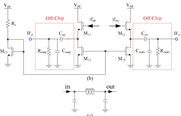
(30) low-noise operation, the size of the switch should be large; however, it inevitably leads to large parasitic nonlinear capacitance at the midpoints of the transconductor and switching quad, introducing signal loss in these nodes and degrading linearity. The optimum gate-source bias of the switch is slightly below the threshold voltage of the NMOSFET. Actually, the switching quad is designed to operate in the weak inversion region to reduce flicker noise.. For measurement purpose, we connect an on-chip common-drain output buffer as shown in Fig. 2.5(b) to simultaneously match IF port to 50Ω and increase output driving capability. Finally, we take advantage of the pi-matching circuit as shown in Fig. 2.5(c) to match LO port to 50Ω and be able to provide sufficient LO power from outside signal generator to mixer.. (a) 19.
(31) (b). (c) Fig. 2.5 (a) Double-balanced sub-harmonic mixer (b) Common-drain output buffer (c) Off-chip matching network of the LO port. Fig. 2.6 Operation of double LO frequency. 20.
(32) 2.2.2 Design Flow In this section, we attempt to systemize the design step of the sub-harmonic mixer.. The current and the minimum overhead voltage are utilized to determine the transistor size and DC bias of the transconductor. The goal in this step is to ensure that the transistor works in saturation region, given a certain variation range for its drain voltage. As discuss in previous sections, noise figure, conversion gain, and linearity are all related to the sizes of the transconductor transistors. Conversion gain and linearity are major consideration initially, but noise figure should be refined later.. The variation range of the drain voltage of the transconductors is determined by taking in account the variation caused by the LO switching activities. It is now time to determine the LO bias voltage and the size of the switching quad. Non-ideal switching behavior, that is, the switches are not completely turned on or off, will reduce the conversion gain, and possibly generates more noise. Similar to the transconductors, the switching quad is designed to work in saturation region, taking the variation of the gate source voltage and the drain voltage into consideration. Note that the preferred variation range of the drain voltage of the switching quad is much larger than that of the transconductor; because we want the IF signal to vary over a large voltage range without causing distortion.. The matching network of the RF port, LO port, and IF port can now be determined for maximum power transmission. In case noise performance cannot be satisfied, the RF port should be matched for optimal noise figure.. 21.
(33) Conversion gain and noise figure, and intermodulation are now obtained. If any of them is not satisfactory, the above procedures are repeated with the adjustment of the DC bias and transistor sizes. These steps form the design flow of the sub-harmonic mixer as shown in Fig. 2.7. Transconductor Size and DC Biasing. Switch Size, DC Biasing and LO Magnitude. RF, LO, IF Impedance Matching. NO. NO. Conversion Gain NF, IIP3 OK?. Verification OK?. Done Fig. 2.7 Design flow of the sub-harmonic mixer. 2.2.3 Circuit Layout After careful design and simulation, the double-balanced sub-harmonic mixer is implemented by using 0.18-µm CMOS 1P6M technology. The final layout is shown 22.
(34) in Fig. 2.8. All elements are fully integrated on a chip including spiral inductors, MIM (metal-insulator-metal) capacitors, multi-finger RF NMOS transistors, and poly resistors. The total chip size including the pads is about 1000× 980 µm2. At the high frequency, the drain and source of a MOSFET, pads, inductors, MIM capacitors, and other elements on the silicon substrate have resistive components due to the lossy silicon substrate. These parasitic resistances consume signal power, generate thermal noise, and thus gain and noise performances of the mixer are degraded a lot. To avoid these effects from the pads, we also take advantage of the shielded signal PAD as shown in Fig. 2.9 to reduce noise coupling from the noisy silicon substrate [17]. We will show its final simulated and measured results later.. The RF and LO signal frequencies are chosen at 5.25GHz and 2.62GHz, respectively. The fact that LO frequency is lower than the center of desired band is called “low-side injection”. Minimizing the LO frequency will facilitate the design of the oscillator. The output IF signal thus falls at 10MHz. Because this design is designed for PCB on-board testing, the parasitic effects of bond-wires and bond-pads will greatly influence the impedance matching of all ports. Only with good input or output impedance matching, the power delivered into the chip or received by the measurement instruments can be more efficiently. Therefore, these parasitic effects must be included and considered throughout all simulation procedure carefully.. The double-balanced sub-harmonic mixer achieves a conversion voltage gain of 8.1 dB (to 1MΩ load), -18.6 dBm P1dB (to 50Ω load), -10.9 dBm IIP3 (to 50Ω load), and 11.5 dB DSB noise figure at 10MHz IF frequency, consuming 3.95 mA from 1.8V supply for the SPICE post simulation.. 23.
(35) Fig. 2.8 Layout of the double-balanced sub-harmonic mixer. Fig. 2.9 Structure of the shielded signal PAD. 2.3 Measurement of Sub-Harmonic Mixer 2.3.1 Measurement Consideration Because the RF input of this mixer is differential, the Balun is required to transform single-ended measurement system into differential. Here, we take the rat-race (180° ring hybrid) shown in Fig. 2.10(a) as a Balun. The ideal [S] matrix of the rat-race will have the following form: ⎡0 1 ⎢ − j ⎢1 0 [S ] = ⎢ 2 1 0 ⎢ ⎣0 −1 24. 1 0⎤ 0 −1⎥⎥ 0 1⎥ ⎥ 1 0⎦.
(36) It can split the input power from port 4 into port 2 and port 3 with equal half power and 180° phase difference. Thus, the measured [S] matrix of the rat-race for the RF port is as follows:. ⎡ 0.106∠113.19° 0.684∠ − 160.52° 0.685∠ − 160.53° 0.016∠ − 56.46° ⎤ ⎢ 0.685∠ − 160.51° 0.087∠103.59° 0.005∠ − 105.69° 0.685∠18.96° ⎥⎥ ⎢ [S ] = ⎢ 0.684∠ − 160.57° 0.005∠ − 106.31° 0.112∠104.32° 0.685∠ − 162.02° ⎥ ⎢ ⎥ 0.684∠18.76° 0.685∠ − 162.20° 0.084∠106.95° ⎦ ⎣ 0.016∠ − 56.79°. (a) (b) (c) Fig. 2.10 Photograph of the (a) RF port rat-race (b) LO port rat-race (c) LO port quadrature hybrid In addition, the LO input of this mixer is quadrature, so two rat-races shown Fig. 2.10(b) combined with a quadrature hybrid shown Fig. 2.10 (c) are required to act as a LO port Balun. The ideal [S] matrix of the quadrature hybrid for the LO port will have the following form: ⎡0 j 1 0⎤ ⎢ ⎥ −1 j 0 0 1 ⎥ [ S ] = ⎢⎢ 2 1 0 0 j⎥ ⎢ ⎥ ⎣0 1 j 0⎦ With all ports matched, power entering port 1 is evenly divided between ports 2 and 3, with a 90° phase shift between these outputs. No power is coupled to port 4 (the isolation port). For the LO port, the measured [S] matrixes of the rat-race and quadrature hybrid are as follows: 25.
(37) [ S ]rat −race. 0.689∠135.4° 0.016∠ − 94.2° ⎤ ⎡ 0.029∠117.4° 0.678∠135.56° ⎢0.678∠135.14° 0.045∠0.2° 0.024∠ − 161.7° 0.675∠ − 42.5° ⎥⎥ =⎢ ⎢0.688∠134.95° 0.023∠ − 162.5° 0.029∠34.6° 0.677∠137.62°⎥ ⎢ ⎥ 0.057∠41.1° ⎦ ⎣ 0.016∠ − 93.8° 0.675∠ − 42.1° 0.678∠138.15°. [ S ]quadrature hybrid. 0.674∠70.05° 0.664∠ − 18.5° 0.047∠ − 4.36° ⎤ ⎡ 0.025∠75.7° ⎢ 0.675∠70.5° 0.026∠99.9° 0.044∠11.4° 0.665∠ − 20.5° ⎥⎥ ⎢ = ⎢ 0.665∠ − 18.15° 0.044∠11.5° 0.039∠76.7° 0.675∠70.9° ⎥ ⎢ ⎥ ⎣ 0.047∠ − 4.25° 0.665∠ − 20.9° 0.675∠70.5° 0.017∠ − 133.5°⎦. Although these experimental results still have little error, they are very close to these of the ideal cases and satisfied for our requirement. Therefore, when all other ports are terminated with matched loads, the measured transmission coefficients of the LO port quadrature Balun composed of two rat-races and quadrature hybrid from port 1 to port 2-port 5 are S 21 = 0.444∠ − 125.75° , S31 = 0.442∠54.82° , S 41 = 0.452∠142.04° , and S51 = 0.452∠ − 35.27° , respectively. The photograph of the LO port quadrature Balun is shown in Fig. 2.11.. Fig. 2.11 Photograph of the LO port quadrature Balun PCB layout and practical FR4 PCB circuit with SMA connectors for this design are shown in Fig. 2.12 and Fig. 2.13, respectively. One important thing must be taken care in the design of the PCB layout, the width of the RF and LO signal paths must be 26.
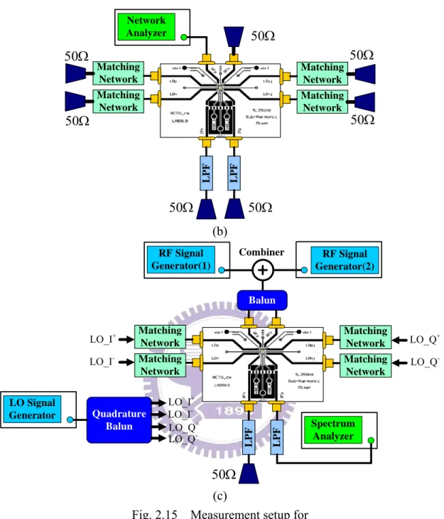
(38) drawn as 50Ω-line width for impedance matching. This chip is adhered to PCB first and all I/O pads on this chip are then bonded to PCB via bond-wires. The die photograph of this chip including bond-wires is shown in Fig. 2.14. Throughout all measurement procedures, we still require extra three signal generators, one spectrum analyzer, one network analyzer, one oscilloscope and other auxiliary devices, such as cables, 50Ω terminals, and power combiners. Since we have finished the prior preparations for the PCB on-board testing, the measurements can now be proceeding according to arrangements in Fig. 2.15. It should be noted that the losses of the cable, Balun, combiner, SMA connectors, and PCB board itself must be taken account for calibration and measurements.. There are some RF parameters that we have to measure in our design of the double-balanced sub-harmonic mixer. These parameters include RF and LO input return loss, conversion voltage gain, P1dB, and two-tone linearity test of IIP3. We have used RFIC measurement systems in the CIC and our laboratory to finish these measurements. The simplified block diagrams of the each measurement setup for each parameter are illustrated in Fig. 2.15.. Fig. 2.12. PCB test board layout of the sub-harmonic mixer. 27.
(39) Fig. 2.13 Practical PCB test board of the sub-harmonic mixer. Fig. 2.14 Die photograph of the double-balanced sub-harmonic mixer RF Signal Generator. LO Signal Generator. Matching Network. LO_Q+. Matching Network. Matching Network. LO_Q-. Quadrature Balun. LO_I+ LO_ILO_Q+ LO_Q-. 50Ω (a) 28. LPF. LO_I-. Matching Network. LPF. LO_I+. Balun. Spectrum Analyzer.
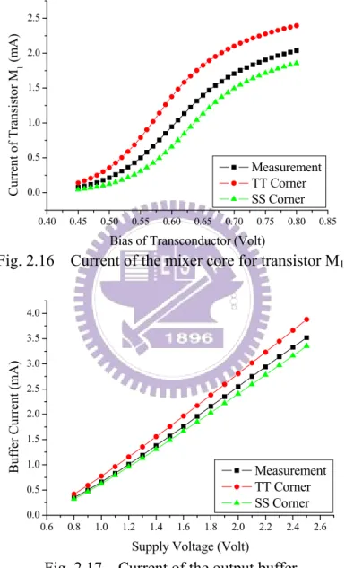
(40) Network Analyzer. 50Ω 50Ω. 50Ω. Matching Network. Matching Network. Matching Network. Matching Network. 50Ω. LPF. LPF. 50Ω. 50Ω. 50Ω (b) Combiner. RF Signal Generator(1). RF Signal Generator(2). Balun. LO Signal Generator. Matching Network. LO_Q+. Matching Network. Matching Network. LO_Q-. Quadrature Balun. LO_I+ LO_ILO_Q+ LO_Q-. LPF. LO_I-. Matching Network. LPF. LO_I+. Spectrum Analyzer. 50Ω (c) Fig. 2.15 Measurement setup for (a) conversion gain (b) input return loss testing (c) two-tone IIP3 testing. 2.3.2 Measurement Results Upon previous measurement considerations and arrangements, we have made all PCB on-board tests for our design in CIC and our laboratory. First of all, we measure the current of the core and buffer, as shown in Fig. 2.16 and Fig. 2.17, respectively. In Fig. 2.16 and Fig. 2.17, they reveal that measured curve is close to SS-corner but not located at TT-corner. This means that the process condition now falls at the vicinity of 29.
(41) SS-corner. Therefore, we will modify simulation to SS-corner to compare with measurement. Note that we have reset the bias condition in SS-corner to get optimum performance. This chip dissipates total power of 9.63mW, including 5.74mW in mixer core and 3.89mW in output buffer, from a 1.8V supply voltage.. Current of Transistor M1 (mA). 2.5 2.0 1.5 1.0 0.5. Measurement TT Corner SS Corner. 0.0 0.40. 0.45. 0.50. 0.55. 0.60. 0.65. 0.70. 0.75. 0.80. 0.85. Bias of Transconductor (Volt). Fig. 2.16 Current of the mixer core for transistor M1 4.0. Buffer Current (mA). 3.5 3.0 2.5 2.0 1.5 1.0. Measurement TT Corner SS Corner. 0.5 0.0 0.6. 0.8. 1.0. 1.2. 1.4. 1.6. 1.8. 2.0. 2.2. 2.4. 2.6. Supply Voltage (Volt). Fig. 2.17 Current of the output buffer In 50Ω measurement system, Fig. 2.18 and Fig. 2.19 show the RF port return loss and LO port return loss, respectively. They reveal measured RF port return loss of 9.14 dB at 5.25 GHz and measured LO port return loss of 6.1 dB at 2.62 GHz. Fig. 2.20 is the conversion power gain under LO power sweep from -17 dBm to 8 dBm,. 30.
(42) where RF power is fixed at -40 dBm. We can see that the maximum measured conversion power gain of -7.4 dB can be obtained while LO power is 0 dBm. The P1dB and two-tone test are shown in Fig. 2.21 and Fig. 2.22, respectively. They reveal that the measured P1dB and IIP3 are -14.2 dBm and -2.3 dBm, respectively. Therefore, this chip achieves the performances of high linearity and wide dynamic range. In these figure above, they show simultaneously the simulation and measurement results. Finally, the output waveform of the IF port is also measured by oscilloscope (1MΩ load), instead of spectrum analyzer (50Ω load). Fig. 2.23 shows that the measured peak-to-peak voltage of IF output waveform is about 203.2 mV while RF and LO input power is –17 dBm and 0 dBm, respectively. Through simple mathematics transformation, this circuit actually performs conversion voltage gain of 1.12 dB. All simulation and measurement performances are summarized in Table 2.1.. 0. Return Loss of RF Port (dB). -1 -2 -3 -4 -5 -6 -7. Measurement Simulation Modify. -8 -9 -10 4.0. 4.5. 5.0. 5.5. 6.0. 6.5. 7.0. Frequency (GHz). Fig. 2.18 RF port return loss of the sub-harmonic mixer. 31.
(43) Return Loss of LO Port (dB). 0. -5. -10. -15. Measurement Simulation Modify. -20. -25 2.2. 2.3. 2.4. 2.5. 2.6. 2.7. 2.8. Frequency (GHz). Fig. 2.19 LO port return loss of the sub-harmonic mixer. Conversion Power Gain (dB). 0 -10 -20 -30 -40 -50. Measurement Simulation Modify. -60 -40. -30. -20. -10. 0. 10. LO Input Power (dBm). Fig. 2.20 Conversion power gain of the sub-harmonic mixer. Converion Power Gain (dB). 0 -5 -10 -15 -20. Measurement Simulation Modify. -25 -30 -50. -40. -30. -20. -10. 0. RF Input Power (dBm). Fig. 2.21 1dB compression point of the sub-harmonic mixer. 32.
(44) 0 -20. IF Output Power (dBm). -40 -60 -80 -100 -120 Fundamental (Measurement) IM3 (Measurement) Fundamental (Simulation) IM3 (Simulation) Fundamental (Modify) IM3 (Modify). -140 -160 -180 -200 -220 -60. -50. -40. -30. -20. -10. 0. 10. RF Input Power (dBm). Fig. 2.22 Third-order-interception point of the sub-harmonic mixer. IFp IFp-p = 203.2mV @RF power = -17dBm LO power = 0dBm. 10MHz IFn. Fig. 2.23 Measured IF output waveform of the sub-harmonic mixer. 2.4 Comparison Table 2.2 shows the comparisons of this work and other recently sub-harmonic mixer papers. According to the simulation parameters, power dissipation of this work is less than all other circuits, but the linearity is poor with nearly equal conversion voltage gain. We must add some linearity technique to improve the linearity in future work. Because the process condition is falling at the vicinity of SS-corner, the measured results are not good as simulated results. Therefore, bias circuit can be integrated into this sub-harmonic mixer in future tape out to ensure that the. 33.
(45) performances are not influenced by process condition. Furthermore, we must base on accurate models and careful simulation to make sure the measurement would close to the simulation.. Table 2.1 Performance Summaries of the sub-harmonic mixer Specification. Simulation. Measurement. Modify. Supply Voltage (Volt). 1.8. 1.8. 1.8. LO Power (dBm). -13. 0. -3. RF Return Loss (dB). 8.1. 9.14. 7.42. LO Return Loss (dB). 14.1. 6.1. 7.3. IF Return Loss (dB). 19.5. N/A. 15. LO-to-RF Isolation (dB). >50. 23.1. >50. 2LO-to-RF Isolation (dB). >50. 53. >50. Conversion Power Gain (dB). 1.3. -7.4. -6.76. Conversion Voltage Gain (dB). 8.1. 1.12. 1.81. P1dB (dBm). -18.6. -14.2. -16.2. IIP3 (dBm). -10.9. -2.3. -6.5. Noise Figure (dB). 11.5. N/A. 14.4. Core. 2.84. 5.74. 4.93. Buffer. 4.26. 3.89. 3.55. Total. 7.1. 9.63. 8.48. Power Consumption (mW). 34.
(46) Table 2.2 Comparison of sub-harmonic mixer [18]. [19]. [20]. Sim.. Sim.. Sim.. Supply Voltage (V). 3. 3. 1.8. 1.8. RF Frequency (GHz). 2. 5.6. 5.6. 5.25. Conversion Voltage Gain (dB). 11.61. 8.01. 8.05. 8.1. 1.12. P1dB (dBm). N/A. -12. -13.5. -18.6. -14.2. IIP3 (dBm). -13.5. -6.5. 0. -10.9. -2.3. Noise Figure (dB). 12. 5.96. N/A. 11.5. N/A. Mixer Current (mA). 1.71. 1.75. 2.6. 1.58. 3.19. 0.25µm. 0.25µm. 0.18µm. CMOS. CMOS. SiGe. Reference Specification. Process. 35. This Work Sim.. Meas.. 0.18µm CMOS.
(47) Chapter 3 CONCURRENT DUAL-BAND RECEIVER FRONT-END USING 0.18µm CMOS. Growing market demands of low cost for present WLAN systems push system architecture from multiple-path-multiple-band to concurrent multiple-band type. By employing a sub-harmonic mixer with an LO signal operating at half of RF frequency, a new concurrent dual-band receiver architecture with only one frequency synthesizer for 802.11a/b/g applications is proposed in Chapter 3. The common properties suggest that the two standards can be accommodated in this concurrent dual-band receiver while sharing some of the components. A concurrent dual-band receiver front-end consisting of a differential concurrent dual-band LNA, a Gilbert mixer, and a sub-harmonic mixer is designed and implemented here.. 3.1 Review of Receiver Architecture 3.1.1 Superheterodyne Receiver Most RF communication transceivers manufactured today utilize the superheterodyne receiver architecture, as shown in Fig. 3.1 [21], consisting of a collection of the discrete components with the different technologies such as GaAs,. 36.
(48) bipolar, and CMOS.. After receiving RF signal, the signal is downed to baseband by two steps down-conversion, each followed by filtering and amplification. As shown in Fig. 3.1, the first mixer down converts the interested band to IF1. After filtering out the unwanted band, the second mixer down converts the desired channel to IF2.. Fig. 3.1 Superheterodyne receiver The superheterodyne receiver usually has the superior performance by taking advantage of the high quality (high-Q) discrete components. However, using these discrete components is the contrary to the goal of the high integration by the modern portable communication equipments. The challenge of fully integrating the superheterodyne receiver is to replace the functions implemented by the high performance, high-Q discrete components with the on-chip components. This causes several problems. First, the quality factors of the on-chip passive components are usually much lower than those of the discrete ones. Low-Q passive components will produce the additional noise and the signal losses due to their parasitic resistances. These low-Q passive components are also difficult to realize the on-chip passive filter to meet the stringent specifications of the image-rejection filter and IF filter. Second, the low-Q inductor also degrades the phase noise of the voltage-controlled oscillator 37.
(49) (VDO). In a conclusion, the superheterodyne receiver is not a suitable solution for integration.. 3.1.2 Direct Conversion Receiver The direct conversion receiver is also named the zero-IF receiver. Obviously, it down-converts the RF signal directly to DC, as shown in Fig. 3.2. Thus, this receiver can eliminate many off-chip filters because it is free from the images. Although the direct conversion receiver allows the high level of integration, it also associates with many problems [22], such as the DC-offsets, even-order distortion, I-Q mismatch, and the flicker noise.. ω. ωRF ω. ωLO = ωRF Fig. 3.2 Direct conversion receiver Due to the isolation between the LO and the RF ports of the mixer is not infinite, large LO signal may couple to the RF port of the mixer. And the LO signal may also radiate to the air and be received by the antenna and input to the RF port of the mixer. These two effects are called the “LO leakage”. Because the frequencies of the LO and the RF signals are the same, this LO leakage will mix with the LO signal, called the “self-mixing”, and produces the unexpected DC term. This DC term may corrupt the information near the DC and also may saturate the stages following the mixer. It is not easy to eliminate this DC offset because it is a time-variant term [23]. Furthermore, the down-converted signal is allocated in the vicinity of the DC, the flicker noise 38.
(50) becomes the determinative noise source. It is crucial to process the baseband signal with the low-noise. The easiest solution is using the larger device sizes.. 3.1.3 Low-IF Receiver One integrated low-IF receiver which alleviates the DC-offset problems is shown in Fig. 3.3. The all desired channels are translated to the IF, which is roughly on the order of one or two channel bandwidth. The primary advantage of a low-IF system is free from the DC-offsets.. Unfortunately, the image-rejection becomes the most difficult problem in the low-IF receiver because the image signal is close to the RF signal. Some image-rejection architectures are employed to filter the image signals, such as Hartley and Weaver image-rejection architectures [24]. Another method to suppress the image signal is using the passive polyphase filter [25].. Due to the few building blocks and no DC-offset problem, the low-IF receiver architecture becomes the most appreciate one in the receiver design. Note that IF should be allocated higher than the corner frequency to reduce the flicker noise.. ωLO Fig. 3.3 Low-IF receiver. 3.2 Design of Concurrent Dual-Band Receiver. 39.
(51) 3.2.1 Architecture By the rapid development and large demand of wireless communication, a fully integration monolithic multi-band radio transceivers are the most significant considerations for communication applications. Wireless LANs provide wideband wireless connectivity between PCs and other consumer electronic devices, allowing access to core networks and other equipment in office and home environments. The commercial WLAN system consists of an RF transceiver together with a base-band and media access controller (MAC) processor. Most of the dual-band receivers now use individual receiving paths shown in Fig. 3.4 but they take large hardware areas. The hardware cost is considerably high if a dual-band receiver is considered with such scheme. The concurrent dual-band receivers should be taken into account. Fig. 3.5 is the receiver consisting of a dual-band concurrent low-noise amplifier (LNA), two mixers, and a multi-modulus frequency synthesizer. These two mixers are sub-harmonic mixer for 5.25 GHz band and Gilbert mixer for 2.45 GHz band, respectively. On-chip intermediate frequency (IF) filter is required in the system. Gm-C filters are used for noise bandwidth limiting and anti-aliasing reasons. As shown in Fig. 3.6, the architecture of the proposed dual-band receiver receives signals at the frequency bands of 2.4 GHz to 2.483 GHz in 802.11b/g and 5.15 GHz to 5.35 GHz, 5.725 GHz to 5.825 GHz in 802.11a; it utilizes single path to receive signals from antenna. A concurrent dual-band receiver front-end consisting of a differential concurrent dual-band LNA, a Gilbert mixer, and a sub-harmonic mixer is designed and implemented here.. 40.
(52) Fig. 3.4 Conventional architecture of a dual-band receiver. Fig. 3.5 Proposed architecture of the concurrent dual-band receiver The architecture and frequency plan of the RF transceiver play an important role in the complexity and performance of the overall system. The common choice in transceiver architecture is the traditional superheterodyne and direct conversion. Direct conversion is a usually choice in a fully integrated design because it avoids the need for an off-chip IF filter and requires only a single frequency synthesizer. However, it suffers from drawbacks such as local oscillator (LO) leakage and frequency pulling due to the fact that the synthesizer operates at the same frequency as the RF signal [23]. The superheterodyne architecture overcomes many of the disadvantages of direct conversion at the expense of an IF filter and an extra frequency synthesizer [21]. A high performance low-IF dual-band receiver is developed with Gm-C filter. The proposed low-IF receiver front-end combines the 41.
(53) advantages of both the classical IF receiver and the zero-IF receiver, which is an excellent performance and a high degree of integration [26]. Such design also applies this receiving architecture without using external components to achieve circuit integrity and efficiency. Finally the IF is chosen at 10 MHz because of the noise and receiver architecture considerations. Fig. 3.7 shows the frequency plan of this receiver front-end.. Fig. 3.6 Receiving band distribution of WLAN in the range of 2.4~6 GHz. Fig. 3.7 Frequency plan of the concurrent dual-band receiver. 3.2.2 Circuit Implementation The challenge of integrating LNA and mixers comes from the inter-stage design. In the design procedure we try to match the output matching of differential dual-band LNA and RF input matching of two mixers to the same impedance, for instance, 500Ω parallel with 100pF, rather 50Ω. Large coupling capacitors are added between LNA. 42.
(54) and mixers for RF signal coupling and DC isolation. A description of each functional unit is provided as follows: A. Dual-Band Low-Noise Amplifier The dual-band LNA is differential inputs in this proposed dual-band receiver front-end. Fig. 3.8 is a schematic of the single-ended dual-band LNA. Two identical single-ended dual-band LNA are paralleled to compose a differential dual-band LNA. In the single-ended dual-band LNA, the inductively source degeneration consists of a bondwire whose center frequency is tuned to 2.45 GHz and 5.25 GHz. The input matching network and output matching network are the LC tank and LC branch, respectively. As shown in Fig. 3.8, the LC tank is used to resonate the gate impedance and provide the additional lower band gain transfer function. The LC branch introduces a zero in the transfer function of the LNA and performs a notch between 2.45 GHz and 5.25 GHz to improve receiver’s image rejection. The detail analyses of the dual-band single-ended LNA can be found in [27].. Fig. 3.8 Single-ended dual-band LNA B. Sub-Harmonic Mixer for 5.25 GHz Band The proposed concurrent dual-band receiver front-end adopts sub-harmonic 43.
(55) mixer as shown in Fig. 3.9 in 5.25 GHz band. As described in Chapter 2, the sub-harmonic mixer is based on the classical Gilbert mixer with a switching quad that can conduct on each half cycle of the driving waveform. Different from Chapter 2, this sub-harmonic mixer set input impedance at 500Ω paralleled with 100pF in order to get maximum transfer power gain from LNA. The detail analysis is same as described in Chapter 2.. Fig. 3.9 Sub-harmonic mixer for 5.25 GHz band C. Gilbert Mixer for 2.45 GHz Band As the conventional receiver, the Gilbert mixer is adopted in 2.45 GHz band in the proposed concurrent dual-band receiver front-end. The sub-harmonic mixer can be served as a Gilbert mixer if LOp port connects with LOn port and LOpj port connects with LOnj port to form two RF inputs and two LO inputs. Therefore, two bands can adopt the same architecture to reduce design complexity. Fig. 3.10 is a Gilbert mixer 44.
(56) which has two RF inputs and two LO inputs. Gilbert mixer has same principles as the sub-harmonic mixer described in Chapter 2. Vdd. RLn. RLp IFp IFn. C4. M3. M7. LOp R3. M4. M8. Vblo R4. M5. M9. LOn C3. M6. RFp. C1. M1. M10. M2. R1. C2. RFn. R2. Vbrf. Vbrf. Fig. 3.10 Gilbert mixer for 2.45 GHz band. 3.2.3 Circuit Layout The proposed concurrent dual-band receiver front-end is designed and optimized using 0.18µm 1P6M CMOS technology. All elements are fully integrated on a chip including spiral inductors, MIM capacitors, multi-finger RF MOS transistors, and poly resistors. Similarly, we also take advantage of shielded signal PAD as described previously to reduce coupling noise from the noisy silicon substrate. In order to minimize the phase and the magnitude errors between the differential signal paths, the lengths of signal paths are kept equal as much as possible. To accomplish the more balance, the dummy lines are also added. Furthermore, guard-ring is used to block the. 45.
(57) coupling noise between the circuits. The final layout and die photo are shown in Fig. 3.11. The total chip size including the pads is about 1450× 1450µm2.. (a) (b) Fig. 3.11 (a) Layout of the concurrent dual-band receiver front-end (b) Die photo of the concurrent dual-band receiver front-end. 3.3 Measurement of Concurrent Dual-Band Receiver 3.3.1 Measurement Consideration The concurrent dual-band receiver front-end is measured by two PCB boards, 2.45 GHz and 5.25 GHz, rather one PCB board, because of large size off chip passive Balun, too many on-board decoupling capacitors, and complicated DC bias routing. Fig. 3.12(a) and Fig. 3.12(b) are the PCB layouts of the dual-band receiver front-end, respectively. Because the LO input is quadrature in 5.25 GHz band, the quadrature Balun, which has been mentioned in section 2.3, is required again for 5.25 GHz receiver front-end measurement. There are some comments on PCB boards design. Firstly the width of RF and LO signal paths on PCB are drawn as 50 Ω-line for impedance matching. Lumped coupling capacitors (1uF) are placed in the RF paths. 46.
(58) for dc isolation. To filter out the ineluctable noise and spur from the power supplies we add four lumped decoupling capacitors between each dc voltage and ground, including 100pF, 10nF, 100nF, and 1uF. IF low-pass-filters composed of lumped capacitors and resistors are placed at the IF outputs to depress the high frequency noise. Therefore, the practical PCB test boards of the dual-band receiver front-end are shown in Fig. 3.13(a) and Fig. 3.13(b), respectively. According to measurement setup of Fig. 3.14, we use RFIC measurement system to measure this chip in CIC.. (a) (b) Fig. 3.12 PCB test board layout of concurrent dual-band receiver front-end for (a) 2.45 GHz band (b) 5.25 GHz band. (a) (b) Fig. 3.13 Practical PCB test board of concurrent dual-band receiver front-end for (a) 2.45 GHz band (b) 5.25 GHz band 47.
(59) DC Supplies. Balun. Signal Generator. RF. chip. Spectrum Analyzer. IF 50Ω. LO 2/4. LO Matching Network. Differential for 2.45GHz Band or Quadrature for 5.25 GHz Band. 2/4. Signal Generator. Balun / Quadrature Balun. Fig. 3.14 Measurement setup of concurrent dual-band receiver front-end. 3.3.2 Measurement Results Upon previous measurement considerations and arrangements, we have made all PCB on-board tests for our design in CIC and our laboratory. In 50Ω measurement system, the measured RF port input return loss of receiver front-end is 15.9 dB and 15.8 dB at 2.45GHz and 5.25GHz, respectively, as shown in Fig. 3.15. The measured LO port input return loss of lower band mixer is 13.4 dB and that of higher band mixer is 13.1 dB, as shown in Fig. 3.16(a) and Fig. 3.16(b), respectively. Fig. 3.17(a) and Fig. 3.17(b) show the measured linearity of the front-end, characterized by the overall RF-to-IF P1dB, are -21 dBm and -15.3 dBm, respectively. Fig. 3.18(a) and Fig. 3.18(b) show the measured dynamic range of the front-end, characterized by the overall RF-to-IF IIP3 for RF signals in two frequency bands, are -4.2 dBm and 4.9 dBm, respectively. Finally, Fig. 3.19 is the IF output waveform measured by oscilloscope. This receiver front-end demonstrates 17.2 dB and 11.8 dB conversion voltage gain at two frequency bands with 28.8 mW power dissipation from a 1.8V supply voltage. The simulated and measured results are summarized in Table 3.1. 48.
(60) Three major factors may depress the gain and increase noise figure of the concurrent dual-band receiver front-end. First, the inter-stage design may be interfered by the parasitic capacitors and resistors, causing the impedance mismatch between the output of differential dual-band LNA and RF input of mixers. Second, the quality factor Q values of the inductors are not good enough due to parasitic resistances. The Q-values of these inductors involved in this work is from 7.08 to 8.27. The gain and output matching of the concurrent dual-band LNA will be seriously affected by the poor Q-value of inductors. Finally the absence of output buffers at IF output impacts the driving capability of the front-end.. Return Loss of RF Port (dB). 0. -5. -10. -15. -20. Measurement Simulation. -25 0. 1G. 2G. 3G. 4G. 5G. 6G. 7G. Frequency (Hz). 5. 5. 0. 0. Return Loss of LO Port (dB). Return Loss of LO Port (dB). Fig. 3.15 RF port return loss of the receiver front-end. -5. -10. -15. -20 2.0G. Measurement Simulation 2.2G. 2.4G. 2.6G. 2.8G. 3.0G. -5. -10. -15. -20 2.0G. Measurement Simulation 2.2G. 2.4G. 2.6G. Frequency (Hz). Frequency (Hz). (a) (b) Fig. 3.16 LO port return loss of the receiver front-end for (a) 802.11b/g band (b) 802.11a band 49. 2.8G. 3.0G.
(61) 10. 16. Conversion Power Gain (dB). Conversion Power Gain (dB). 14 12 10 8 6 4 2 0. Measurement simulation. -2 -4 -40. -35. -30. 5 0 -5 -10 -15. Measurement Simulation. -20 -25. -20. -15. -40. -10. -35. RF Input Power (dBm). -30. -25. -20. -15. -10. RF Input Power (dBm). (a) (b) Fig. 3.17 1-dB compression point of the receiver front-end for (a) 802.11b/g band (b) 802.11a band 0. 20. IF Output Power (dBm). IF Output Power (dBm). 0. -20. -40. Fundamental (Measurement) IM3 (Measurement) Fundamental (Simulation) IM3 (Simulation). -60. -80 -30. -25. -20. -15. -10. -5. -20. -40. -60 Fundamental (Measurement) IM3 (Simulation) Fundamental (Measurement) IM3 (Simulation). -80 0. -30. RF Input Power (dBm). -25. -20. -15. -10. -5. 0. RF Input Power (dBm). (a) (b) Fig. 3.18 Third-order-interception point of the receiver front-end for (a) 802.11b/g band (b) 802.11a band. 10MHz. 10MHz IFp. IFp IFp-p = 234.4mV @RF power = -16.72dBm. IFp-p = 248.4mV @RF power = -25.35dBm. IFn. IFn. (a) (b) Fig. 3.19 Measured IF output waveform of the receiver front-end for (a) 802.11b/g band (b) 802.11a band 50. 5.
(62) Table 3.1 Performance summaries of the dual-band receiver front-end Specification. 2.45GHz Front-End. 5.25GHz Front-End. Sim.. Meas.. Sim.. Meas.. LO Power (dBm). 3. 8. -3. 7. RF Return Loss (dB). -18.4. 15.9. -13.4. 15.8. LO Return Loss (dB). -13.2. 13.4. -18.3. 13.1. Conversion Gain (dB). 14.7. 6.0. 2.57. -12.0. Voltage Gain (dB). 26.5. 17.2. 19.9. 11.8. Noise Figure (dB). 3.77. 7.22. 7.28. 10.78. P1dB (dBm). -20.6. -21.0. -22.1. -15.3. IIP3 (dBm). -7.8. -4.2. -4.5. 4.9. Supply Voltage (V). 1.8 Simulation : 17.6. Power Consumption (mW). Measurement : 28.8. 3.4 Comparison Table 3.2 shows the comparisons of this work and other recently dual-band receiver front-end papers. Compared with other dual-band receiver front-end this work achieves comparable performances with nearly equal chip area and lower power dissipation under concurrent operation for two frequency bands.. 51.
數據
+7

相關文件
接收器: 目前敲擊回音法所採用的接收 器為一種寬頻的位移接收器 其與物體表
Comparison of B2 auto with B2 150 x B1 100 constrains signal frequency dependence, independent of foreground projections If dust, expect little cross-correlation. If
z 香港政府對 RFID 的發展亦大力支持,創新科技署 06 年資助 1400 萬元 予香港貨品編碼協會推出「蹤橫網」,這系統利用 RFID
請繪出交流三相感應電動機AC 220V 15HP,額定電流為40安,正逆轉兼Y-△啟動控制電路之主
An OFDM signal offers an advantage in a channel that has a frequency selective fading response.. As we can see, when we lay an OFDM signal spectrum against the
This reduced dual problem may be solved by a conditional gradient method and (accelerated) gradient-projection methods, with each projection involving an SVD of an r × m matrix..
The major testing circuit is for RF transceiver basic testing items, especially for 802.11b/g/n EVM test method implement on ATE.. The ATE testing is different from general purpose
傳統的 RF front-end 常定義在高頻無線通訊的接收端電路,例如類比 式 AM/FM 通訊、微波通訊等。射頻(Radio frequency,
