國 立 交 通 大 學
電子工程學系 電子研究所 碩士班
碩 士 論 文
考慮在電源雜訊環境下休眠電晶體置放之低功
率平面規劃
Floorplanning with Sleep Transistors Insertion in the
Presence of Power Supply Noise for Low Power
研 究 生:葉志益(Chih-Yi Yeh)
指導教授: 陳宏明 教授(Prof. Hung-Ming Chen)
考慮在電源雜訊環境下休眠電晶體置放之低功率平面
規劃
Floorplanning with Sleep Transistors Insertion in the
Presence of Power Supply Noise for Low Power
研 究 生:葉志益 Student:Chih-Yi Yeh
指導教授:陳宏明 教授 Advisor:Professor Hung-Ming Chen
國 立 交 通 大 學
電 子 工 程 學 系 電 子 研 究 所 碩 士 班
碩 士 論 文
A Thesis
Submitted to Department of Electronics Engineering & Institute of Electronics
College of Electrical and ComputerEngineering
National Chiao Tung University
in Partial Fulfillment of the Requirements
for the Degree of Master
in
Electronics Engineering
October 2006
Hsinchu, Taiwan, Republic of China
考慮在電源雜訊環境下休眠電晶體置放之低功
率平面規劃
學生:葉志益 指導教授:陳宏明 博士 國立交通大學 電機工程學系 電子研究所 碩士班 摘 要近來隨著製程不斷的進步,晶片的面積與工作頻率都能做得很好,而
低功率卻成為現今最熱門的問題。高臨界電壓的電晶體由於其特性被
用來限制電路的漏電流現象,來減少電路在非工作時間裡所損耗的功
率,這種特殊的電晶體我們稱為休眠電晶體。然而以往休眠電晶體只
應用在極少的地方上,直到最近才被重視而成為相當熱門的研究話
題。本論文則是研究如何決定在哪些電路裡插入電晶體才會節省到功
率;以及在做平面規劃時,如何將休眠電晶體所需要的面積考慮進
去。實驗結果顯示我們的方法是有效的,可以得到一個考慮電源雜
訊,並放置休眠電晶體的低功率平面規劃。
Floorplanning with Sleep Transistors Insertion in
the Presence of Power Supply Noise for Low
Power
Student:Chih-Yi Yeh Advisor:Hung-Ming Chen
Department of Electronics Engineering Institute of Electronic Engineering
National Chiao Tung University
Abstract
As the technology scales, the chip area and the working frequency can be done very well. However, low power becomes the most hot topic. High threshold voltage
transistors are used to limit the leakage current to reduce the unnecessary power when the circuit is idle. And this high threshold voltage transistors are called sleep
transistors. However sleep transistor is used in few application in the past, and now it becomes a hot topic. This thesis research how to decide which modules are really need to be inserting sleep transistors, and how to design enough area for sleep transistor when we do the floorplan. The experimental results show our method can work, and we can get a low power floorplan with sleep transistor insertion in the presence of power supply noise.
致 謝
能夠完成這篇論文,最感謝的是我的指導教授陳宏明博士,教授
不但在我學習中細心低教導,傳授了我許多關於 EDA 以及程式語言
方面的知識,也在我撰寫本篇論文時耐心低協助與適時低給予意見,
讓我能夠完成此論文。
感謝實驗室的同學們平常跟我在課業上切磋琢磨,在生活上的鼓
勵與幫助。
Floorplanning with Sleep Transistors Insertion in
the Presence of Power Supply Noise for Low Power
Prepared by Chih-Yi Yeh
Directed by Prof. Hung-Ming Chen
Department of Electronics Engineering
National Chiao Tung University
Hsinchu, Taiwan 300, R.O.C.
2006-10
Contents
1 Introduction 1
1.1 Our Contribution . . . 2
1.2 Organization of this Thesis . . . 2
2 Preliminaries 3 2.1 Sleep Transistor . . . 3
2.1.1 Sleep Transistor Insertion and Sizing . . . 3
2.1.2 Power Supply Noise Effect on Sleep Transistor . . . 4
2.1.3 Cost Evaluation on Sleep Transistor Insertion . . . 5
2.2 Power Supply Distribution and Power Supply Noise Calculation . . . 6
2.3 Floorplan Representations . . . 8
2.3.1 Review of the Sequence Pair Representation . . . 8
2.3.2 Review of the B*-tree Representation . . . 9
2.4 Problem Formulation . . . 11
3 Methodology for Integrating Floorplann and Sleep Transistor Siz-ing in the Presence of Power Supply Noise 12 3.1 Power Evaluation . . . 12
3.2 Sequence Pair Packing . . . 13 3.3 B*-tree Packing . . . 16
4 Experimental Results 22
4.1 Power Analysis Results . . . 22 4.2 Floorplan Results . . . 23
5 Conclusion 27
List of Figures
2.1 Sleep transistor. (a)NMOS type (b)PMOS type . . . 4 2.2 The circuit block current I(t) flows the power resistance R, and causes
a voltage drop ∆v = I(t)×R . . . 5 2.3 Power saving and cost by sleep transistor[1]. (a) The module is asleep
in tsleep and active in tactive (b) The leakage power dissipation before
and after inserting sleep transistor, ∆P1 is saved by sleep transistor.
(c) The dynamic power dissipation before and after inserting sleep transistor, ∆P2 is the extra cost due to sleep transistor. . . 7
2.4 The assuming power supply system in this thesis. The power bumps (small black circles) are uniformly distributed in the chip. Modules (a, b) drain current only from their nearby power bump, and suffer power supply noise. . . 8 2.5 (a) Oblique grid for sequence pair (X,Y) = ((a b d e c f) , (c b f a d
e))(b) The corresponding packing.[2][3] . . . 9 2.6 (a) In horizontal constraint graph Gh(V, E), a path hs→ a→ d→ e→
ht corresponds to <a d e>, a common subsequence of (X,Y) = ((a b
d e c f) , (c b f a d e)) (b) In vertical constraint graph Gv(V, E), a
path vs→ f→ e→ vt corresponds to <f e>, a common subsequence
2.7 (a) An admissible placement. (b) The corresponding B*-tree[4][5] representation. . . 11 3.1 Horizontal longest common sequence evaluation process on Sequence
pair ((a,b,d,e,c,f),(c,b,f,a,d,e))[3]. . . 15 3.2 The floorplan of Sequence pair ((a,b,d,e,c,f),(c,b,f,a,d,e)) . . . 15 3.3 (a) The floorplan width is less than the height. (b) Re-do the H-LCS
and increase the width of those gating modules (b, d, f)[3]. . . 16 3.4 (a) The flowchart of simulated annealing framework[6] with inserting
sleep transistors in sequence pair packing . . . 17 3.5 (a) The present floorplan and the horizontal contour. (b)block b3 will
be placed on the top of block b1, the y-coordinate can be got from the
horizontal contour. (c) Place the b lock b3 and update the horizontal
contour[5]. . . 19 3.6 (a) Place the most left-bottom module to its location. (b) Calculate
the noise and size the sleep transistor if need. (c) Place the next module and insert sleep transistor if need. (d) Continue the work. (e) The whole floorplan . . . 20 3.7 (a) The flowchart of simulated annealing framework[6] with inserting
sleep transistors in B*-tree packing . . . 21 4.1 floorplan of ami33 based on sequence pair packing. The small black
block represents the power bumps, and the dark area represents the sleep transistor. . . 25 4.2 floorplan of ami33 based on B*-tree packing. The small black block
represents the power bumps, and the dark area represents the sleep transistor. . . 25
List of Tables
4.1 The result of power simulator. . . 23 4.2 Compare the power consumption in MCNC benchmark, circuit ami33
and circuit ami49. . . 23 4.3 The floorplanning results of ami33 with sequence pair packing and
B*-tree packing. . . 24 4.4 The floorplanning results of ami49 with sequence pair packing and
Chapter 1
Introduction
Low power is an important issue in modern VLSI design. As the technology scales, we have faster and smaller devices. However, at the same time, the sub-threshold effect of CMOS becomes more and more apparent so that the power consuming of leakage current takes a high proportion of chip power.
Power-gating is an effective technique for saving leakage power by inserting a sleep transistor to shutting off the idle blocks [7]. According to [8][9] we can size the sleep transistor according to the current of the corresponding module. And [10][11] consider the physical placement and introduce distributed sleep transistor network to save the silicon area of sleep transistor. While we consider the effect of power supply noise, we must revise the formula to achieve an enough area for inserting sleep transistor [12][13]. However, the cost of transistor is very high, so we must carefully evaluate the efficiency of sleep transistor to avoid the negative effects [1].
Besides, there are many other topics about sleep transistor. For example, [14] did the research about wake-up schedule of sleep transistor to save the power con-sumption when the asleep circuits wake up. And [15] provided a flow to help design a circuit with power-gating technique. [16] researched the synthesis of sleep transis-tor. [17] applied the sleep transistor in a low-leakage twin-precision multiplier and [18] applied sleep transistor in sram.
1.1
Our Contribution
In this thesis, we introduce the sleep transistor technique into the floorplan to lower the leakage power producing by those idle modules. And we develop a low power floorplanning framework by considering sleep transistor in the presence of power supply noise. Our framework determines which modules can employ sleep transistors to save leakage, and decide the size as well.
1.2
Organization of this Thesis
In Chapter 2, we will introduce how does sleep transistor save leakage power and how to size it. And then describe the relation between sleep transistor and power supply noise. We also briefly review the sequence-pair representation [2] and B*-tree representation [4] and give the problem formulation. In Chapter 3, we discuss our method for evaluating ,sizing the sleep transistor, and integrate them into floorplan. Our experimental results are presented in Chapter 4. Finally we give the conclusion of this thesis and future work in Chapter 5.
Chapter 2
Preliminaries
In this chapter, we introduce the sleep transistors and how to size. We also introduce how do power supply noise effect sleep transistors. Then we briefly review two kinds of floorplan representation, sequence pair and B*-tree. In the end, we formulate the problem, integrated floorplanning and sleep transistor sizing in the presence of power supply noise.
2.1
Sleep Transistor
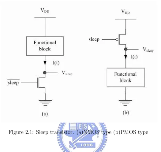
Power gating is a technique for saving leakage power by inserting a high threshold voltage transistor, sleep transistor, between the circuit and power supply network, as shown in Figure 2.1. When the sleep transistor is turned on, the circuit works normally with an extra delay causing by the additional sleep transistor. When the sleep transistor is turned off, the circuit can not work because the sleep transistor cuts off the power supply. Thus, the circuit comes into sleep mode and consumes less leakage power which is reduced by the high threshold voltage transistor.
2.1.1
Sleep Transistor Insertion and Sizing
To size the sleep transistor, first we should notice that the sleep transistor is in series with the circuit block. So the sleep transistor must be large enough to allow the
Figure 2.1: Sleep transistor. (a)NMOS type (b)PMOS type
maximum current of the circuit flowing it, or it will limit the current to a smaller value and then increase the circuit delay. Hence, we have
(W
L)st =
Imax
δµnCox(Vdd− VtL)(Vdd− VtH)
where Imaxis the maximin current in the low Vtcircuit, VtH is the threshold voltage
of sleep transistor and is higher than VtL in the low Vt circuit, and δ is performance
loss described in [10]. Performance loss δ can be set to an suitable value so that the total circuit delay is acceptable.
2.1.2
Power Supply Noise Effect on Sleep Transistor
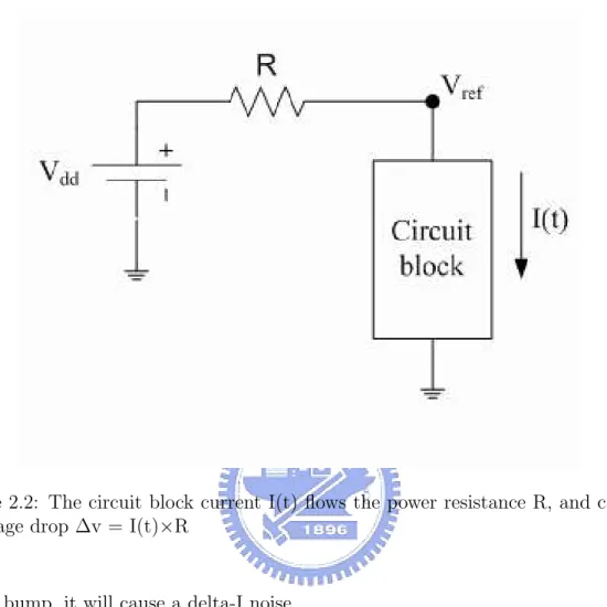
Power supply noise comes from the non-ideal power supply network, and there are two principal source, IR drop and delta-I noise. When the current flows from the power bump to the power ping of circuit, the resistance of power supply network makes a voltage drop, as shown in Figure 2.2. While we consider the inductance of
Figure 2.2: The circuit block current I(t) flows the power resistance R, and causes a voltage drop ∆v = I(t)×R
power bump, it will cause a delta-I noise.
While we consider the effect of power supply noise, the formula of sleep transistor must be revised to
(W
L)st =
Imax
δµnCox(Vref − VtL)(Vref − VtH)
where Vref = Vdd - Vnoise
2.1.3
Cost Evaluation on Sleep Transistor Insertion
The purpose of sleep transistor is to save leakage power when the circuit blocks are idle. However, sleep transistor itself will consume power. If the cost is equals to or even larger than the savings, then the sleep transistor is not worth. Refer to the work in [1], we can calculate the saving and the cost of sleep transistor.
active time, tr and twake−up are the switching time. Figure 2.3(b) and (c) shows the
leakage power and dynamic power of circuits with sleep transistor. The bold line illustrates the power consumed in the chip with sleep transistor inserted, and the light line illustrates power consumed in the chip without sleep transistor. From the comparisons, we have that ∆P1 is the leakage power saved by sleep transistor, and
∆P2 is the dynamic power overhead.
The power dissipation in tr is very small since the power supply is disconnected
by the sleep transistor. When the module is in sleep mode, the internal node of the circuit will be charged to VDD. Before the module returns to active mode, it need
a wake-up time twake−up to discharge the internal node. We define Ewake−up to be
the energies dissipated by sleep transistor during the wake-up time twake−up. The
Ewake−up depends on it corresponding module and can be calculated according to
the total capacitance of all internal nodes[14] in the module. To ensure the sleep transistor worthwhile, the following inequality must be satisfied
∆P1· tsleep > ∆P2· (tsleep+ tactive) + Ewake−up
From the above inequality, we note that the sleep time should be long enough, and the active time cannot be too long. This indicates that circuit modules with long sleep time and short active time are suited to insert sleep transistor. However those modules which switch between sleep mode and active mode frequently are not suited to insert sleep transistor, because their consume to much Ewake−up.
2.2
Power Supply Distribution and Power Supply
Noise Calculation
In this thesis, we assume that the package is flip-chip bounding, and the power bump is distributed in the whole chip. The power supply network is resistive. Modules draw current only from their nearby power bump and suffer a IR-drop noise and we
Figure 2.3: Power saving and cost by sleep transistor[1]. (a) The module is asleep in tsleep and active in tactive (b) The leakage power dissipation before and after
inserting sleep transistor, ∆P1 is saved by sleep transistor. (c) The dynamic power
dissipation before and after inserting sleep transistor, ∆P2 is the extra cost due to
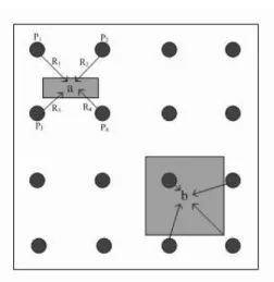
Figure 2.4: The assuming power supply system in this thesis. The power bumps (small black circles) are uniformly distributed in the chip. Modules (a, b) drain current only from their nearby power bump, and suffer power supply noise.
do not consider the delta-I noise. Figure 2.4 illustrates the power supply distribution. Module a draws current from its nearby four power bumps. The resistance between module a and power bump P1 is R1 = d × ρ, where d is the distance between
module a and power bump P1 and ρ is the wire resistance of power supply network.
Then the power supply noise of module a is Vnoise = (R1kR2kR3kR4) × Ia. Hence
modules suffer more power supply noise if they are father away the power bumps. However the size of sleep transistor depends on the power supply noise, the sleep transistor area will vary according the position of its corresponding module.
2.3
Floorplan Representations
Floorplan represent is used to transform between geometric graph and algebraic meanings. In this thesis we choose two represents, sequence pair and B*-tree.
2.3.1
Review of the Sequence Pair Representation
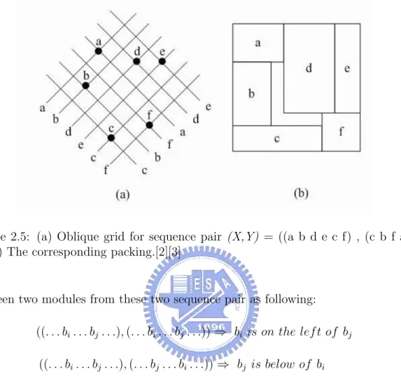
A sequence pair [2] is a pair of module-name sequences like ((a,b,d,e,c), (c,b,a,d,e)), where a,b,c,d,e represents a module respectively. We can know the relationship
Figure 2.5: (a) Oblique grid for sequence pair (X,Y) = ((a b d e c f) , (c b f a d e))(b) The corresponding packing.[2][3]
between two modules from these two sequence pair as following: ((. . . bi. . . bj. . .), (. . . bi. . . bj. . .)) ⇒ bi is on the lef t of bj
((. . . bi. . . bj. . .), (. . . bj. . . bi. . .)) ⇒ bj is below of bi
Figure 2.5 illustrates the grid and the corresponding packing. First we translate the sequence pair into the grid graph. From the grid, we can know the approximate location of each module and establish a horizontal graph and a vertical graph, as shown in Figure 2.6. And then place all modules into their locations according to the horizontal and vertical graphs. However, [3] introduces a better method to find out the positions of all modules quickly, in which a data structure, bucket list, is used to evaluate sequence pair in O(n log log n) time.
2.3.2
Review of the B*-tree Representation
A B*-tree [4] is an ordered binary tree whose root corresponds to the module on the bottom-left corner for modeling a non-slicing floorplan. Given a admissible place-ment which every module can neither move down nor move left, we can construct a
Figure 2.6: (a) In horizontal constraint graph Gh(V, E), a path hs→ a→ d→ e→ ht
corresponds to <a d e>, a common subsequence of (X,Y) = ((a b d e c f) , (c b f a d e)) (b) In vertical constraint graph Gv(V, E), a path vs→ f→ e→ vt corresponds
to <f e>, a common subsequence of (XR,Y) = ((f c e d b a) , (c b f a d e))[2][3].
unique B*-tree in linear time. Further, given a B*-tree, we can also obtain an ad-missible placement by packing the blocks in a linear time with a contour structure [5].
In a B*-tree T, the root of T represents the block on the bottom-left corner; i.e. the x - and y-coordinates of the block associated with root (xroot, yroot) = (0,0). If
node nj is the left child of node ni, block bj is placed on the right-hand side and
adjacent to block bi in the admissible placement; i.e. xj = xi + wi, where wi is the
width of block bi. Otherwise, if node nj is the right child of node ni, block bj is
placed above block bi with equivalent x -coordinate; i.e. xj = xi. With the contour
structure, we can compute the y-coordinate of block bj in constant time.
Figure 2.7 illustrates an admissible placement and its corresponding B*-tree representation. Use the depth-first search (DFS) procedure, we can recursively construct the admissible placement. First, we pick the root n0 and place block
b0 on the bottom-left corner. Then we traverse the left child of n0, n1, and place
Figure 2.7: (a) An admissible placement. (b) The corresponding B*-tree[4][5] rep-resentation.
its right child n3 and place block b3 above block b1. Continue the process until all
nodes are traversed, and finally we will get an admissible placement.
2.4
Problem Formulation
The problem we concerned is described as follows. Let M = {m1,m2,. . . ,mn} be
a set of n rectangular modules. Each module has its height hi, width wi, and
switching profile including the active time and idle time, the dynamic and leakage power dissipation, the wake-up time, and the wake-up power dissipation. The goal is to evaluate whether a module needs to insert sleep transistor or not, and to find a optimal floorplan with minimum cost (in area, wire-length), and arrange enough area for modules with sleep transistor under the effect of power supply noise.
Chapter 3
Methodology for Integrating
Floorplann and Sleep Transistor
Sizing in the Presence of Power
Supply Noise
In this chapter, we introduce our methodology to do this work. For a given design, first we should evaluate which modules should be inserted with sleep transistors. Once we make sure which modules need to be gated, we size the area of sleep transistors and do the floorplanning. While doing the floorplanning, we will calculate the noise and revise the area of sleep transistors. After these steps, we complete our work.
3.1
Power Evaluation
To ensure the benefit of sleep transistor, first we should compute the power dissi-pation of every module before and after inserting sleep transistor. And then decide whether we should insert sleep transistor to this module or not. To accomplish this work, we must prepare the profile of modules. This must includes the active and idle time, the dynamic and leakage power dissipation, the wake-up time, and the wake-up power dissipation.
First we assume every module is inserted with sleep transistor. And there are three conditions for computing the power dissipation. (1)When the module is in active mode, it consumes dynamic power and the energy is Eactive = Pdynamic ×
Tactive. (2)When the module is in idle mode, we first check if Tidle > Twake−up. If it
is true, this module can enter the sleep mode, and then it consumes leakage power and the energy is Esleep = Pleakage × Tsleep. Otherwise this module can not enter
sleep mode since it has no time to sleep. Thus it must stay in active mode and it consumes dynamic power with energy Eactive = Pdynamic × Tidle. (3)When the
module is entering active mode from sleep mode, it will consume the wake-up power and the energy is Ewake−up = Pwake−up × Twake−up, where Ewake−up is discussed in
Chapter 2.1.3.
Then the power dissipation is Pgated = (Eactive + Esleep + Ewake−up) / Ttotal.
Compared with the original power Poriginal, if Pgated < Poriginal, this module is worth
being gated. Otherwise we should not insert sleep transistor to this module. Thus we can know whether we can get advantage or not if we insert sleep transistor into a module. Once we make sure which modules is suitable to insert sleep transistor, we go to the next step, floorplan. There are many representation for packing floorplans, in this thesis we choose sequence pair and b*-tree representation. And we use the simulated annealing framework[6] to accomplish the floorplan.
3.2
Sequence Pair Packing
In sequence pair packing, there are two processes to establish the floorplan, hori-zontal longest common subsequence pair evaluation (H-LCS ) and vertical longest common subsequence pair evaluation (V-LCS ).
subsequence in X and Y. We use the data structure, bucket-list[3], to help to find the longest common sequence more efficiently. The bucket-list is composed of double-linked node. And the node has three data, x 1 = x 2last−node represents the
x -coordinate of this module, x 2 = x 1 + module width, represents the x -coordinate
of next module which is right to this module, and bucket-list number represents the sequence position in Y.
In this process, modules will be placed from left to right and their x -coordinates will be determined. As shown in Figure 3.1, we will search every element in sequence
X, and find the bucket-list number according to the sequence Y. For example, the
first element in sequence X is a, and its bucket-list is 4 since a is the forth element in sequence Y. And x 1(a) is set to 0 since its last node, root, x 2(0) = 0. Then the
x 2(a) is set to x 1(a) + width(a) (Figure 3.1 (b)). The second element in X is b
and its bucket-list number is 2. This node will be inserted between node 0 and node 4, and x 1(2) = x 2(0) = 0, x 2(2) = x 1(2) + width(b). (Figure 3.1(c)). The following two element in X, d and e, are the same. (Figure 3.1 (d)). When we insert the fifth element in X, c, whose bucket-list number is 1, into the bucket-list, we check every node after it and delete the node whose x 1 is less than x 2(c). This means those deleted nodes are not component of longest common subsequence. (Figure 3.1(e)). Final we complete the process and determine the x 1 of all modules. (Figure 3.1(f)) And vertical longest common subsequence pair evaluation (V-LCS) is similar to H-LCS. But this will place modules form bottom to up, orientate the y-coordinates. After these two processes we get the floorplan as shown in Figure 3.5. The location of a module can be sure after we complete these two processes. Thus we can analysis the power supply noise and size the sleep transistor. But the locations of modules are fixed, and there may be no space to insert sleep transistor.
To solve this problem, our method is, compare the weight and height of this floorplan. If the weight is less than height, we re-do the H-LCS and increase the
Figure 3.1: Horizontal longest common sequence evaluation process on Sequence pair ((a,b,d,e,c,f),(c,b,f,a,d,e))[3].
Figure 3.3: (a) The floorplan width is less than the height. (b) Re-do the H-LCS and increase the width of those gating modules (b, d, f)[3].
weight of modules for inserting sleep transistor, otherwise we redo the V-LCS and increase the height of modules, as shown in Figure 3.3.
We use simulated annealing framework [6] to obtain a acceptable solution. In simulated annealing process, we perturb the original sequence pair to obtain a new sequence pair. Then we pack the new floorplan and calculate the new cost. If the new cost is less than the original cost, we will accepted this new floorplan. We do this process repeatedly until we obtain an accepted solution or the temperature of simulated annealing cools down. The flowchart is shown in Figure 3.4.
3.3
B*-tree Packing
In B*-tree packing, we will do the depth-first-search (DFS) on the tree and place the module corresponding the node which we are visiting. While we are placing block
bj, first we check that node nj is a left or right child of his father, node ni. If it is a
left child, the x -coordinate is set to be xj = xi + wi, where wi is the width of block
Figure 3.4: (a) The flowchart of simulated annealing framework[6] with inserting sleep transistors in sequence pair packing
same as its father.
After we determine the x -coordinate, we will use the horizontal contour[5] to find out the x -coordinate of that module. The horizontal contour is a vector that records the top line of present floorplan, and will be updated if a module is placed into the floorplan, as shown in Figure 3.5.
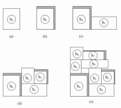
Unlike sequence pair packing, B*-tree will always place the most left-bottom modules first. Thus when we place a module into the floorplan, other modules which is bellow or left to it have been placed already. So we can place this module and make sure its location. Then we calculate the power supply noise and size the sleep transistor. After we get the area of sleep transistor, we add this area into the module. Here we do not increase only its width (or height) alone. We will increase both the width and height and keep the ratio of the module the same, as shown in Figure 3.6. We use the simulated annealing to obtain an acceptable solution and the flowchart is shown in Figure 3.7
Figure 3.5: (a) The present floorplan and the horizontal contour. (b)block b3 will
be placed on the top of block b1, the y-coordinate can be got from the horizontal
Figure 3.6: (a) Place the most left-bottom module to its location. (b) Calculate the noise and size the sleep transistor if need. (c) Place the next module and insert sleep transistor if need. (d) Continue the work. (e) The whole floorplan
Figure 3.7: (a) The flowchart of simulated annealing framework[6] with inserting sleep transistors in B*-tree packing
Chapter 4
Experimental Results
We implement a power simulator to evaluate which modules are suitable to be inserted sleep transistor, and two floorplanners; one is based on sequence pair pack-ing and another is based on B*-tree packpack-ing. All above are implemented in C++ programming language. The platform is Intel Pentium 3.0GHz CPU with 2.0GB memory. We experiment with our approach on MCNC[19] circuit benchmark. And we refer to the tsmc 0.18 CMOS library to model our sleep transistor. We will compare the power consumption before and after inserting sleep transistor, and the result of sequence pair packing and B*-tree packing.
4.1
Power Analysis Results
We do the experiment on ami33 and ami49, the circuit benmark of MCNC. The results are shown in Table 4.1 and Table 4.2. In ami33, before we insert the sleep transistor, its original power is 161.7mW, including dynamic power 125.7mW and leakage power 36mW. Our simulator choose 10 modules to insert sleep transistor (because these module will consume less power if they have sleep transistors). The area of these 10 modules is 32.10% of ami33. After we insert the sleep transistor, its total power 157.6mW, including dynamic power 127.96mW and leakage power 29.73mW.
Table 4.1: The result of power simulator. number of area of gated total area of Circuit
gated modules modules (nm2) circuit (nm2) percentage
ami33 10 3.68×10⁵ 1.15×10⁶ 32.10 %
ami49 29 1.30×10⁷ 3.53×10⁷ 36.68 %
Table 4.2: Compare the power consumption in MCNC benchmark, circuit ami33 and circuit ami49.
Without Sleep transistor With Sleep Transistor Circuit
total dynamic leakage total dynamic leakage
ami33 161.7 125.7 36 157.69 127.96 29.73
ami49 254.3 193.5 50.8 237.3 197.8 39.5
In ami49, before we insert the sleep transistor, its original power is 254.3mW, in-cluding dynamic power 193.5mW and leakage power 50.8mW. Our simulator choose 29 modules to insert sleep transistor (because these module will consume less power if they have sleep transistors). The area of these 29 modules is 36.68% of ami49. After we insert the sleep transistor, its total power 237.3mW, including dynamic power 197.8mW and leakage power 39.5mW.
The dynamic power increases because sleep transistors will consume extra dy-namic power when the module is in active mode. But sleep transistor will save leakage power when the circuit is in sleep mode.
4.2
Floorplan Results
After power analysis, we take the results to do the floorplan. In ami33 there is 10 modules chosen to be gated, takes 30.09% of total area. In ami49 there is 29 modules chosen to be gated, takes 36.68% of total area.
Table 4.3: The floorplanning results of ami33 with sequence pair packing and B*-tree packing.
width height area dead space sleep transistor
packing
(nm) (nm) (nm) ratio (%) area (%)
sequence pair 1484 1082.75 1.6×10⁶ 0.73 28.6 3.58
B*-tree 1045 1251.9 1.3×10⁶ 0.83 8.76 3.52
Table 4.4: The floorplanning results of ami49 with sequence pair packing and B*-tree packing.
width height area dead space sleep transistor
packing
(nm) (nm) (nm) ratio (%) area (%)
sequence pair 7177.64 8679.73 6.23×10⁷ 0.82 40 2.40
B*-tree 7275.1 5672.9 4.13×10⁷ 0.78 10.84 3.66
In sequence packing, the floorplan of ami33 has 28.6% dead space, and sleep transistors take 3.58% of total area (see Figure 4.1). The floorplan of ami49 has 40% dead space, and sleep transistor take 2.40% of total area, as shown in Table 4.3. In B*-tree packing, the floorplan of ami33 has 8.76% dead space, and sleep transistors take 3.52% of total area (see Figure 4.2). The floorplan of ami49 has 10.84% dead space, and sleep transistor take 3.66% of total area (see Figure 4.3), as shown in Table 4.4
In this experiment, we use the same time to run the programs based on sequence pair packing and B*-tree packing. According to the results, B*-tree has less dead space than sequence pair. In sequence pair packing, we add the width or height of gated modules for inserting sleep transistor, but the gated modules will push their nearby modules and make a lot of modules. In the other hand, the modules cannot hold its original ratio since we only increase its weight or height. Due to these reasons, the B*-tree packing is suggested to do this work.
Figure 4.1: floorplan of ami33 based on sequence pair packing. The small black block represents the power bumps, and the dark area represents the sleep transistor.
Figure 4.2: floorplan of ami33 based on B*-tree packing. The small black block represents the power bumps, and the dark area represents the sleep transistor.
Chapter 5
Conclusion
In this thesis, we have developed a framework to integrate floorplanning and sleep transistor insertion and sizing in the presence of power supply noise. We use sequence pair and B*-tree as our core engines to perform floorplanning. The experimental results have shown that the B*-tree packing is more suitable to do this work. We further validate the effectiveness of sleep transistor insertion in saving leakage power. Although the application of sleep transistors is few, they are expected to be widely used in the near future due to lower power demand.
Bibliography
[1] Hailin Jiang, Malgorzata Marek-Sadowska, and Sani R. Nassif. “Benefits and Costs of Power-Gating Technique”. In Proceedings IEEE International
Confer-ence on Computer Design, 2005.
[2] Murata, Fujiyoshi, Nakatake, and Kajitani. “Rectangle-Packing Based Mod-ule Placement”. In Proceedings IEEE/ACM International Conference on
Computer-Aided Design, 1995.
[3] Xiaoping Tang and D.F. Wang. “FAST-SP:A Fast Algorithm for Block Place-ment basced on Sequence Pair”. In Proceedings IEEE Asia and South Pacific
Design Automation Conference, 2001.
[4] Y.-C. Chang, Y.-W. Chang, G.-M. Wu, and S. W. Wu. “B*-Trees: A new representation for non-slicing floorplans”. In Proceedings IEEE/ACM Design
Automation Conference, pages 458–463, April 2000.
[5] Guang-Ming Wu, Yun-Chih Chang, and Yao-Wen Chang. “Rectilinear Block Placement Using B*-Trees”. In ACM Trans. on Design Automation of
Elec-tronic Systems, April 2003.
[6] S. Kirkpatrick, C.D. Gelatt, and M. P. Vecchi. “Optimization by simulated annealing”. In Science, pages 671–680, 1983.
[7] Benton H. Calhoun, Frank A. Honor´e, and Anaatha P. Chandrakasan. “A Leakage Reduction Methodology for Distributed MTCMOS”. In IEEE Journal
of Solid State Circuit, May 2004.
[8] Vishal Khandelwal and Ankur Srivastava. “Leakage Control Through Fine-Grained Placement and Sizing of Sleep Transistors”. In Proceedings IEEE/ACM
International Conference on Computer-Aided Design, 2004.
[9] Anand Ramalingam, Bin Zhang, Anirudh Degan, and Daid Z. Pan. “Sleep Transistor Sizing Using Timing Criticality and Temporal Currents”. In
Pro-ceedings IEEE Asia and South Pacific Design Automation Conference, 2005.
[10] Changbo Long, and Lei He. “Distributed Sleep Transistor Network for Power Reduction”. In IEEE Transactions on Very Large Scale Integration (VLSI)
Systems, September 2004.
[11] Pietro Babighian, Luca Benini, Alberto Macii, and Enrico Macii. “Post-Layout Leakage Power Minimization Based on Distributed Sleep Transistor Insertion”. In ProceedingsInternational Symposium on Low Power Electronics and Design, 2004.
[12] Ramaprasath Vilangudipitchai and Poras T. Balsara. “Decap Aware Sleep Transistor Design”. In Proceedings of the 2004 IEEE Dallas/CAS Workshop
Implementation of High Performance Circuits, pages 171–175, 2004.
[13] Ramaprasath Vilangudipitchai and Poras T. Balsara. “Power Switch Network Design for MTCMOS”. In IEEE Transactions on Very Large Scale Integration
(VLSI) Systems, 2005.
[14] Afshin Abdollahi, Farzan Fallah, and Massoud Pedram. “An Effective Power Mode Transition Technique in MTCMOS Circuit”. In Proceedings IEEE/ACM
[15] Kaijian Shi. “Dual threshold voltages and power-gating design flows offer good results”. In EDN, February 2006.
[16] Changbo Long, Jinjun Xiong, and Lei He. “On Optimal physical Synthesis of Sleep Transistors”. In Proceedings International Symposium on Physical Design, 2004.
[17] Magnus Sj¨alander, Mindaugas Drazdziulis, Per Larsson-Edefors, and Henrik Eriksson. “A Low-Leakage Twin-Precision Multiplier Using Reconfigurable Power Gating”. In Proceedings Internationl Symposium on Circuits and
Sys-tems, 2005.
[18] Narendra Vallepalli, Yih Wang, B. Zheng, Kevin Zhang, Uddalak Bhattacharya, Zhanping Chen, Fatih Hamzaoglu, Daniel Murray and Mark Bohr. “SRAM De-sign on 65-nm CMOS Technologh With Dynamic Sleep Transistor for Leakage Reduction”. In IEEE Journal of Solid State Circuit, December 2004.
[19] http://www.cse.ucsc.edu/research/surf/gsrc/mcncbench.html.
[20] Mohab Anis, Shawki Areibi, Mohamed Mahmoud and Mohamed Elmasry. “Dy-namic and Leakage Power Reduction in MTCMOS Circuits Using an Auto-mated Effcient Gate Clustering Technique”. In Proceedings IEEE/ACM Design
![Figure 2.3: Power saving and cost by sleep transistor[1]. (a) The module is asleep in t sleep and active in t active (b) The leakage power dissipation before and after inserting sleep transistor, ∆P 1 is saved by sleep transistor](https://thumb-ap.123doks.com/thumbv2/9libinfo/8652922.194156/19.918.193.703.260.873/figure-transistor-asleep-leakage-dissipation-inserting-transistor-transistor.webp)
![Figure 2.7: (a) An admissible placement. (b) The corresponding B*-tree[4][5] rep- rep-resentation.](https://thumb-ap.123doks.com/thumbv2/9libinfo/8652922.194156/23.918.195.703.155.464/figure-admissible-placement-corresponding-tree-rep-rep-resentation.webp)
![Figure 3.1: Horizontal longest common sequence evaluation process on Sequence pair ((a,b,d,e,c,f),(c,b,f,a,d,e))[3].](https://thumb-ap.123doks.com/thumbv2/9libinfo/8652922.194156/27.918.193.706.164.693/figure-horizontal-longest-common-sequence-evaluation-process-sequence.webp)
![Figure 3.4: (a) The flowchart of simulated annealing framework[6] with inserting sleep transistors in sequence pair packing](https://thumb-ap.123doks.com/thumbv2/9libinfo/8652922.194156/29.918.195.706.272.932/figure-flowchart-simulated-annealing-framework-inserting-transistors-sequence.webp)
![Figure 3.7: (a) The flowchart of simulated annealing framework[6] with inserting sleep transistors in B*-tree packing](https://thumb-ap.123doks.com/thumbv2/9libinfo/8652922.194156/33.918.193.703.186.1023/figure-flowchart-simulated-annealing-framework-inserting-transistors-packing.webp)
