國 立 交 通 大 學
電子工程學系電子研究所
博 士 論 文
應變金氧半場效電晶體機械應力萃取與其相關物理
模型建立之研究
Mechanical Stress Assessment and Physical Model
Development in Strained MOSFETs
研 究 生 : 謝振宇
指導教授 : 陳明哲 博士
應變金氧半場效電晶體機械應力萃取與其相關物理
模型建立之研究
Mechanical Stress Assessment and Physical Model
Development in Strained MOSFETs
研 究 生:謝振宇 Student: Chen-Yu Hsieh
指導教授:陳明哲 博士 Advisor: Dr. Ming-Jer Chen
國立交通大學
電子工程學系 電子研究所
博士論文
A Dissertation
Submitted to Department of Electronics Engineering &
Institute of Electronics
College of Electrical Engineering and Computer Science
National Chiao-Tung University
in Partial Fulfillment of the Requirements
for the Degree of Doctor of Philosophy
in
Electronics Engineering
April 2009
Hsinchu, Taiwan, Republic of China
中華民國九十八年四月
i
應變金氧半場效電晶體機械應力萃取與其相關物理
模型建立之研究
研究生:謝振宇 指導教授:陳明哲 博士
國立交通大學 電子工程學系 電子研究所
摘要
Abstract in Chinese
近來,金氧半場效電晶體中機械應力已引起大量的注意,特別是在電性(如:載子遷 移率、驅動能力及漏電流)及物理現象(如:摻雜擴散及介電層缺陷)的改變。因此本論文 將會展示如何評估元件中各處應力量值。接著,在處理上述議題時,相對應的理論模型 或分析將可被建立基於提出的方法之上。 首先,針對具有1.27奈米閘極氧化層且經由佈局技巧所產生的通道方向應力的n型金 氧半場效電晶體進行導帶電子直接穿隧電流量測。藉由已知製程參數及已發表形變位能 常數,計算不同電壓下閘極電流變化百分比可以得到通道平均應力量值。為驗證此法的 精確性,在相同元件上進行載子遷移率的量測。所產出的壓阻係數與發表的數值高度相 符。而佈局技巧也同時成功藉由經驗公式所檢驗。 其次,利用不同的通道寬度,量測在具有壓縮應力淺溝槽絕緣層下的閘極穿隧電流。 每單位通道寬度之閘極電流隨著寬度下降,呈現增加的趨勢。在這窄縮的方向,兩個基 本的效應須同時考慮:一為在淺溝槽絕緣層邊緣的寬度修正,另一為增長的通道應力。 為了區別此兩因素,一個新的解析寬度依存閘極穿隧電流模型已被成功的建立及使用。 而所得到的寬度修正效應在較為窄小的元件中,相較應力具有壓倒性的重要。然而,對 於較寬的元件,此兩效應的影響是相當的。萃取出之寬度修正量值及應力大小可以直接 重現汲極電流變化。特別的是,寬度修正與應力對閘極電流的影響趨勢相同,但對汲極ii 電流影響相反。 再者,不同閘極邊緣至淺溝槽絕緣層寬度下元件的次臨界電流被量測並轉換成源極/ 汲極延伸區應力值。此萃取出的局部應力大小與在相同元件上,藉由閘極穿隧電流及載 子遷移率所評估的通道應力趨勢相符。閘極邊緣穿隧電流可以直接導出閘極與延伸區重 疊長度的量值。特別是,在壓縮應力下造成摻雜擴散縮短的長度及應變引發的活化能量 值與製程模擬結果相符。亦成功建立一個以物理導向的解析模型,將側向擴散長度表為 延伸區應力的函式。 最後,在p型通道金氧半場效電晶體上的低頻雜訊量測得出:隨淺溝槽絕緣層拉伸應 力在寬度方向的增加將會導致氧化層界面缺陷的減少。在此,兩種可能的物理緣由被提 出:在氧化過程中,(一)較為鬆弛的介面應變;以及(二)單位面積下較為減少的過量矽 原子。
iii
Mechanical Stress Assessment and Physical Model
Development in Strained MOSFETs
Student: Chen-Yu Hsieh Advisor: Dr. Ming-Jer Chen
Department of Electronics Engineering and Institute of Electronics
National Chiao-Tung University
Abstract in English
Recently, mechanical stress in MOSFETs has gained much attention due to significant changes in electrical performance (mobility, drive capability, leakage etc.) and process issues (dopant diffusion, gate oxide integrity etc.). Therefore, this dissertation is aimed at demonstrating how to measure stress quantities in each part of the devices and address the induced changes. Based on the proposed methods, the underlying physical framework can be established while meeting the above issues.
We first measure the conduction-band electron direct tunneling current through 1.27-nm gate oxide of n-MOSFETs that undergo longitudinal stress via a layout technique. With known process parameters and published deformation potential constants as input, fitting of the measured direct tunneling current versus gate voltage leads to channel stress. To examine the accuracy of the method, a link with the mobility measurement on the same device is conducted. The resulting piezoresistance coefficient is shown to be in good agreement with literature values. The layout technique used is validated as well.
Then, gate direct tunneling current under STI compressive stress is measured in a wide range of the drawn gate width W (= 0.11, 0.24, 0.6, 1.0 and 10 μm). The apparent gate current per unit width exhibits an increasing trend with decreasing W. In this narrowing direction, two
iv
fundamentally different effects are encountered: One of the delta width (ΔW) near the STI
edge and one of the enhanced STI stress in the channel. To distinguish between the two effects, a new analytical width-dependent direct tunneling model is developed and applied. Reasonable agreement with data is achieved. The resulting delta width effect is found to dominate over the stress effect especially in the narrow devices, while for the wide ones, they will be comparable. The extracted ΔW and the underlying channel stress (with the
uncertainties identified) straightforwardly produce a good fitting of the drain current variation counterpart. Specifically, it is justified that the delta width and STI stress are co-operative in constituting gate current variation but both have opposite effects on the drain current one.
Third, drain subthreshold current is measured as a function of the gate edge to STI spacing and is transformed into the source/drain extension corner stress. The extracted local stress is quantitatively reasonable with those of the channel as created by the gate direct tunneling measurement in inversion, and the mobility measurement. In addition, its dependencies on the gate edge to STI spacing confirm the validity of the layout technique in controlling the stress. The gate edge direct tunneling (EDT) measurement in accumulation straightforwardly leads to the quantified gate-to-source/drain-extension overlap length. Particularly, a retarded diffusion length and the resulting strain-induced activation energy both are in satisfactory agreement with those of the process simulation. A physically oriented analytic model is therefore reached, expressing the lateral diffusion length as a function of the corner stress.
Finally, low-frequency noise measurement on p-channel MOSFETs yields the density of the gate-oxide interface states, exhibiting a decreasing trend with increasing STI tensile stress in the channel width direction. Two plausible physical origins of the interface-state density suppression in narrow devices are proposed: relaxed interface strain and reduced excess silicon per unit area during the thermal oxidation.
v
Acknowledgement
First of all, I would like to thank my advisor, Professor Ming-Jer Chen, for his guidance and support throughout my doctorate studies. Moreover, I was also deeply affected by his passion and persistence on academic research. Also, special thanks go to Dr. Chin-San Hou for great efforts that I can find a job before receiving the degree.
I would also like to thank my dissertation readers, Professor Jenn-Gwo Hwu, Professor Mong-Song Liang, Dr. Wen-Chin Lee, Professor Shu-Tong Chang, Professor Bing-Yue Tsui, Professor Horng-Chih Lin, and Professor Ming-Jer Chen, for being on committee and providing valuable feedback on this research.
Industrial collaborations have made this research possible. I wish to show my appreciation to Dr. Wen-Chin Lee, Dr. Yi-Ming Sheu, and Mr. Da-Wen Lin at Taiwan Semiconductor Manufacturing Company for providing the test devices, insightful opinions and discussions.
The department of material science and engineering of NTHU and institute of electronics engineering of NCTU have delivered me not only the base knowledge for my research but also a truly delightful learning experience. I would like to express thanks to all of the scholars who helped expand my knowledge in their classes and lectures. Also, I would like to acknowledge Prof. Shu-Tong Chang in NCHU for giving me suggestion on this work.
My life and this work are enriched by the research colleagues of NCTU, and I want to thank them, including both past and current members. It has been an exceptional experience working together with them.
I also express my gratitude to my friends for their companionship and friendship. These have always helped me to move forward with confidence and a smile.
Last but not least, I am deeply grateful to my parents and girl-friend for their love, wisdom, encouragement, and never-ending support. Completing this research and my study
vi
vii
誌謝
首先,誠摯的感謝指導教授陳明哲博士多年以來的細心指導及大力支持。除此之外, 我深受老師對求學問的熱情與堅持所感動。同時,感謝師母侯錦珊博士的熱心及努力, 能讓我在取得學位之前找到理想工作。 特別感謝論文口試委員胡振國教授、梁孟松教授、李文欽博士、張書通教授、崔秉 鉞教授、林鴻志教授以及陳明哲教授在百忙之中給予寶貴的建議及指教。 與工業界的合作使得這份研究得以進行。感謝台灣積體電路製造公司李文欽博士、 許義明博士和林大文先生提供測試元件、寶貴的意見及討論。 清華大學材料科學工程學系與交通大學電子研究所不僅提供我研究的基礎知識還有 快樂的學習時光。感謝所有豐富我見聞的學者。同時,感謝中興大學張書通教授不吝分 享他在此領域的經驗與心得。 研究的夥伴為我的生活及工作增添了色彩。我希望在這感謝他們,不論是以前或現 在的成員。能跟他們共事是一種特殊的經歷與緣份。 感謝我的朋友,這份情誼總是讓我充滿自信與愉悅的往前邁進。 最後,我要深深感謝我的父母長久以來的愛、鼓勵和無盡的支持及女友的陪伴。沒 有他們,這份研究是不可能完成的。這本論文,獻給他們。viii
Contents
Abstract in Chinese ... i
Abstract in English ... iii
Acknowledgement ... v
Contents ... viii
Figure Captions ... xi
Table Lists ... xiv
Chapter 1 Introduction ... 1
1.1 Overview and Motivation ... 1
1.2 Goal ... 2
1.3 Dissertation Organization ... 3
References ... 5
Chapter 2 Strain Effect on Band Structure ... 8
2.1 Review of Mechanics of Materials ... 8
2.1.1 Stress and Strain ... 8
2.1.2 Stress-Strain Relationship ... 11
2.2 Strain-induced Energy Splitting ... 12
References ... 15
Chapter 3 Measurement of Channel Stress Using Gate Direct Tunneling Current in Uniaxially Stressed n-MOSFETs ... 20 3.1 Introduction ... 20 3.2 Experiment ... 21 3.3 Stress Extraction ... 22 3.4 Confirmative Evidence ... 24 3.5 Conclusion ... 25 References ... 26
ix
Chapter 4 Distinguishing Between STI Stress and Delta Width in Gate Direct Tunneling
Current of Narrow n-MOSFETs ... 35
4.1. Introduction ... 35
4.2 Experiment ... 36
4.3 Data Fitting and Parameter Extraction ... 36
4.4 Confirmative Evidence and Discussion ... 38
4.5 Conclusion ... 39
References ... 40
Chapter 5 Electrical Measurement of Local Stress and Lateral Diffusion Near Source/Drain Extension Corner of Uniaxially Stressed n-MOSFETs ... 47
5.1 Introduction ... 47
5.2 Experiment ... 48
5.3 Corner Stress Extraction and Validation ... 48
5.4 Lateral Diffusion Extraction and Confirmation ... 50
5.5 Conclusion ... 54
References ... 55
Chapter 6 Effect of STI Mechanical Stress on p-Channel Gate Oxide Integrity ... 69
6.1 Introduction ... 69 6.2 Experiment ... 69 6.3 Results ... 70 6.4 Physical Origins ... 71 6.5 Conclusion ... 71 References ... 72
Chapter 7 Conclusions and Future Work ... 80
7.1 Conclusions ... 80
7.2 Recommendation for Future Work ... 81
x
xi
Figure Captions
Chapter 2
Fig. 2.1 (a) Schematic of an arbitrary force ΔF acting on an infinitesimal area ΔA, along with the
resolved components: normal ΔFN and shear terms ΔFS. (b) A cubic element located within a
continuous body with stress tensor components shown. ... 18
Fig. 2.2 Two-dimensional geometric deformation of an infinitesimal material element. ... 19
Chapter 3
Fig. 3.1 Device formation process flow. ... 29
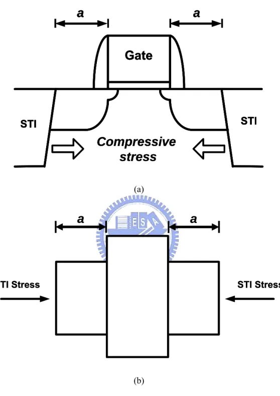
Fig. 3.2 (a) Schematic cross section and (b) topside view of the device under study. The gate edge to STI sidewall, a, is highlighted. The stress condition is compressive due to the lower thermal expansion rate of STI oxide compared to silicon. ... 30
Fig. 3.3 The relative change of the gate direct tunneling current at Vg = 1V versus gate to STI spacing.
The inset shows the mobility variations versus the gate to STI spacing. ... 31
Fig. 3.4 The relative change of the gate direct tunneling current versus extracted uniaxial compressive channel stress for Vg = 0.5, 0.75, and 1V. The symbols are experimental data. The fitting line is drawn
only for accommodating the trend. ... 32
Fig. 3.5 The measured mobility change versus extracted stress. Fitting the data yields the value of piezoresistance coefficient π = -33.5 × 10 -12 dyne-1 cm2. ... 33
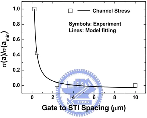
Fig. 3.6 The extracted stress, divided by that of the minimum a, versus the gate to STI spacing, along with a fitting curve from Eq. (3.4). ... 34
Chapter 4
Fig. 4.1 The cross-sectional view of the device in the channel width direction, which can be schematically drawn from the existing simulated device structure in a state-of-the-art manufacturing process [4.3]. The effective channel width designated Weff is the drawn width W plus the delta width
ΔW. ... 42
Fig. 4.2 The relative change of the apparent gate current per unit width at Vg = 1V versus drawn gate
xii
μm, the delta width effect contributes 52% while the remaining (7.3%) stems from the stress induced SiO2/Si barrier lowering. The combination of both effects produces a 63% change in the apparent gate
current density. For sufficiently large W, however, the delta width and channel stress effects become comparable. ΔW = 58 nm, σx = -107 MPa, and k = 130 MPa. ... 43
Fig. 4.3 Comparison of experimental data (symbols) corresponding to Fig. 4.2 with the calculated results. ΔW = 58 nm, σx = -107 MPa, and with k from 0 to 300 MPa. ... 44
Fig. 4.4 Calculated gate and drain current change versus σx (from -70 to -150 MPa) at W = 0.11 μm
relative to the nominal σx (= -107 MPa) at the reference W = 10 μm. The formulas used are inserted.
ΔW = 58 nm and k = 130 MPa. ... 45
Fig. 4.5 The relative change of the apparent drain current per unit width at Vd = 1V and Vg = 1V
versus drawn gate width, along with the calculated results. Note that the piezoresistance coefficients used are the typical bulk values, which are close to those of the inversion-layer ones of state-of-the-art strained n-MOSFETs [4.12], valid only for the channel <110> direction on (001) wafer as studied in this work. ... 46
Chapter 5
Fig. 5.1 The measured subthreshold current change versus gate to STI spacing. ... 60
Fig. 5.2 Measured threshold voltage shift versus gate to STI spacing. ... 61
Fig. 5.3 The extracted mobility variations and source/drain extension corner stress versus gate to STI spacing. ... 62
Fig. 5.4 The plot showing the extracted channel and corner stress, divided by that of the minimum a, versus the gate to STI spacing, along with fitting curves from the citation [5.25]. ... 63
Fig. 5.5 Plot of the measured substrate current versus negative gate voltage. ... 64
Fig. 5.6 Band diagram drawn along n+ poly-gate/SiO
2/diffusion extension. ... 65
Fig. 5.7 Comparison of calculated and measured edge direct tunneling current versus negative gate voltage. ... 66
Fig. 5.8 The extracted gate to source/drain extension overlap length versus gate to STI spacing. The decreasing trend with decreasing a can be related to the retarded lateral diffusion under the influence of the compressive stress. ... 67
xiii
Fig. 5.9 The extracted (symbols) extension overlap length change versus corner stress. Also shown is a fitting line from Eq. (5.11). ... 68
Chapter 6
Fig. 6.1 Measured drain saturation current enhancement factor versus channel width. The inset shows the schematic illustration of STI mechanical stress in the width direction. ... 74
Fig. 6.2 Normalized experimental drain current noise spectral density versus gate overdrive for different channel widths. ... 75
Fig. 6.3 Square root of measured input-referred noise voltage spectral density versus gate overdrive. 76
Fig. 6.4 Extracted effective interface-state density from Fig. 6.3. ... 77
Fig. 6.5 Extracted effective scattering coefficient from Fig. 6.3. ... 78
Fig. 6.6 Schematic illustration of the distribution of the excess species in an oxide film during oxidation [6.9]. ... 79
xiv
Table Lists
Chapter 2
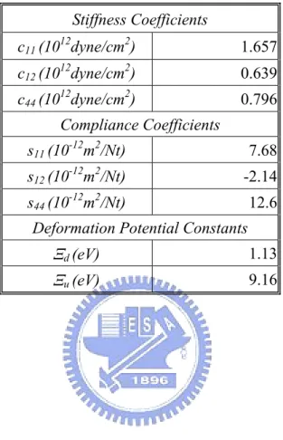
Table 2.1 Compliance and stiffness coefficients, Luttinger parameters, deformation potential constants, and split-off energy for silicon. ... 17
1
Chapter 1
Introduction
1.1 Overview and Motivation
During the quest for increasing device density in integrated circuits, many problems are encountered and need to be solved. As some problems are alleviated, new issues emerge. One of the problems gaining importance in silicon fabrication is process-induced mechanical stress. Many of the processes used in silicon IC fabrication individually and cooperatively contribute to the development of stress in the silicon active areas. Of prime interest is the mechanical stress generated in the isolation process flow. Shallow Trench Isolation (STI) is steadily becoming the predominant isolation technology and is continually challenged as design rules are scaled further [1.1]. One practical topic associated with this trend is that the STI induced mechanical stress in the active region can be controlled with the layout design. This drives the study forward.
Effects of mechanical stress can be divided into two categories: (1) energy band shift and (2) physical behavior modification during the manufacturing process. For the first issue, it is well known that stress can alter the energy structure, which in turn, affects the electrical performance such as the mobility [1.2]–[1.4], the threshold voltage [1.5], and the gate direct tunneling current [1.6]–[1.8]. These properties are strongly related to strain-induced band distortion and warping which actually change the energy level, population, effective mass, and scattering time in each valley. As for the second part, stressed or strained regions have also been shown to influence the physical behaviors like the hot carrier immunity [1.9], the diffusion of dopants [1.10]–[1.12], and the gate oxide integrity [1.13]–[1.15]. Such
2
phenomena were closely contributed by point defects migration and bonding relaxation under different stress conditions. All of above are the major concerns either during manufacturing or in operation. Thus, systematic connection and clarification between the status or magnitude of stress and its physical characteristics in a certain device are urgent and crucial.
1.2 Goal
Mechanical stress influences the physical mechanisms in the fabrication process as well as device operation. Such areas may include point defect diffusion kinetics, extended interfacial defect interactions, and band structure modification. Thus, an accurate stress evaluation is necessary for further investigation of its effects. The goal of this work is primarily to develop a technique where stress can be obtained from the electrical measurement. Once the STI stress in the system is understood, stress or strain dependent models can be established to clarify contradictory issues. Stress evaluation also is helpful in the development and analysis of isolation process technologies.
Dopant diffusion changes have become more prominent recently as a result of increasing mechanical stress in magnitude as the dimensions of the MOSFET are scaled down. Traditionally, the final doping profile prediction is utilized by technology aided-computer design (TCAD) and it may consume a lot of time due to the complexity of transistor structure. However, an approach to immediately reflecting the control of diffusion was still lacking. Thus, another goal of this research is to construct a stress or strain induced diffusion model to trace back the degree of dopant migration with the help of edge direct tunneling.
One of the goals is to clarify the influence of tensile and compressive stress on gate oxide integrity. Such results can relate to reliability issues. All of these would give useful insight into the next generation transistor design involved with the stress effects.
3
1.3 Dissertation Organization
The purpose of this work focuses on the assessment of the STI stress quantities as well as the physical model establishment. Based on the extracted values and status of stress, we can extend the issues to modeling of strain-induced dopant diffusion and gate oxide integrity. At this point, this dissertation is organized into seven chapters.
Chapter 2 begins with the mechanics of materials. The definitions of stress and strain are first reviewed. Their dependencies on each other are associated with the elasticity. Meanwhile, the theory of strain-induced energy band shift both on conduction and valence bands is introduced and will be used in later chapters.
As for the main parts of the dissertation, first of all, we present a simple method to electrically assess the average mechanical stress in channel region using the gate direct tunneling current changes. In this study, shallow trench isolation-induced mechanical stress can serve as the dominant source in the channel due to the thermal expansion and the layout technique will be utilized to produce a variety of stress. The different approaches to determining stresses in longitudinal and transverse directions were detailed in Chapter 3 and 4, respectively. Confirmative evidence is verified by piezoresistance coefficient. Especially, in the narrowing direction, the delta width effect together with the stress effect is adopted to clarify the anomalous trend of gate tunneling current.
Second, in Chapter 5, we show how to transform the drain subthreshold current change to the source/drain corner stress. With the modeling of edge direct tunneling current, it leads to the underlying gate-to-source/drain extension overlap length. Therefore, a physically-oriented analytic model is successfully established, expressing the lateral diffusion as a function of corner stress.
4
In Chapter 6, low-frequency noise measurement will be conducted to extract the oxide integrity in the channel narrowing direction in Chapter 6. Using the stress extraction technique built in previous chapters, the effect of stress on interface states during the oxidation will be demonstrated.
Finally, Chapter 7 delivers a conclusion to the research work, and also addresses the future work as extension of this dissertation.
5
References
[1.1] H. A. Rueda, “Modeling of mechanical stress in silicon isolation technology and its influence on device characteristics,” Ph.D. Dissertation, University of Florida, 1999.
[1.2] J. Welser, J. L. Hoyt, and J. F. Gibbons, “NMOS and PMOS transistors fabricated in strained silicon/relaxed silicon-germanium structures,” in IEDM Tech. Dig., 1992, pp. 1000–1002.
[1.3] S. E. Thompson, M. Armstrong, C. Auth, M. Alavi, M. Buehler, R. Chau, S. Cea, T. Ghani, G. Glass, T. Hoffman, C. H. Jan, C. Kenyon, J. Klaus, K. Kuhn, Z. Ma, B. Mcintyre, K. Mistry, A. Murthy, B. Obradovic, R. Nagisetty, P. Nguyen, S. Sivakumar, R. Shaheed, L. Shifren, B. Tufts, S. Tyagi, M. Bohr, and Y. El-Mansy, “A 90-nm logic technology featuring strained-silicon,” IEEE Trans. Electron Devices, vol. 51, pp. 1790–1797, Nov. 2004.
[1.4] C. H. Ge, C. C. Lin, C. H. Ko, C. C. Huang, Y. C. Huang, B. W. Chan, B. C. Perng, C. C. Sheu, P. Y. Tsai, L. G. Yao, C. L. Wu, T. L. Lee, C. J. Chen, C. T. Wang, S. C. Lin, Y. C. Yeo, and C. Hu, “Process-strained Si (PSS) CMOS technology featuring 3D strain engineering,” in IEDM Tech. Dig., 2003, pp. 73–76.
[1.5] J. S. Lim, S. E. Thompson, and J. G. Fossum, “Comparison of threshold-voltage shifts for uniaxial and biaxial tensile-stressed n-MOSFETs,” IEEE Electron Device
Lett., vol. 25, pp. 731–733, Nov. 2004.
[1.6] A. Hamada, T. Furusawa, N. Saito, and E. Takeda, “A new aspect of mechanical stress effects in scaled MOS devices,” IEEE Trans. Electron Devices, vol. 38, pp. 895–900, Apr. 1991.
[1.7] W. Zhao, A. Seabaugh, V. Adams, D. Jovanovic, and B. Winstead, “Opposing
6
strain,” IEEE Electron Device Lett., vol. 26, pp. 410–412, Jun. 2005.
[1.8] X. Yang, J. Lim, G. Sun, K. Wu, T. Nishida, and S. E. Thompson, “Strain-induced changes in the gate tunneling currents in p-channel metal–oxide–semiconductor field-effect transistors,” Appl. Phys. Lett., vol. 88, pp. 052108, Jan. 2006.
[1.9] J. S. Lim, X. Yang, T. Nishida, and S. E. Thompson, “Measurement of conduction band deformation potential constants using gate direct tunneling current in n-type metal oxide semiconductor field effect transistors under mechanical stress,” Appl.
Phys. Lett., vol. 89, pp. 073509, Aug. 2006.
[1.10] M. J. Aziz, Y. Zhao, H.-J Gossmann, S. Mitha, S. P. Smith, and D. Schiferl, “Pressure and stress effects on the diffusion of B and Sb in Si and Si-Ge alloys,” Phys. Rev. B, vol. 73, p. 054101, Feb. 2006.
[1.11] S. T. Dunham, M. Diebel, C. Ahn, and C. L. Shih, “Calculations of effect of anisotropic stress/strain on dopant diffusion in silicon under equilibrium and nonequilibrium conditions,” J. Vac. Sci. Technol. B, vol. 24, pp. 456-461, Jan./Feb. 2006.
[1.12] M. J. Chen and Y. M. Sheu, “Effect of uniaxial strain on anisotropic diffusion in silicon,” Appl. Phys. Lett., vol. 89, p. 161908, Oct. 2006.
[1.13] E. Simoen, G. Eneman, P. Verheyen, R. Delhougne, R. Loo, K. De Meyer, and C. Claeys, “On the beneficial impact of tensile-strained silicon substrates on the low-frequency noise of n-channel metal-oxide-semiconductor transistors,” Appl.
Phys. Lett., vol. 86, p. 223509, May 2005.
[1.14] M. P. Lu, W. C. Lee, and M. J. Chen, “Channel-width dependence of low-frequency noise in process tensile-strained n-channel metal-oxide-semiconductor transistors,”
7
[1.15] A. Stesmans, P. Somers, V. V. Afanas'ev, C. Claeys and E. Simoen, “Inherent density of point defects in thermal tensile strained (100)Si/SiO2 entities probed by electron spin resonance,” Appl. Phys. Lett., vol. 89, p. 152103, Oct. 2006.
8
Chapter 2
Strain Effect on Electronic Band Structure
2.1 Review of Mechanics of Materials
The property of solid materials to deform under the application of an external force and to regain their original shape after the force is removed is referred to as its elasticity. The external force applied on a specified area is known as stress, while the amount of deformation is called the strain. In this section, the theory of stress, strain and their interdependence is briefly discussed.
2.1.1 Stress and Strain
Stress - Stress is the distribution of internal body forces of varying intensity due to
externally applied forces [2.1], [2.2]. Consider a general body subjected to forces acting on its surface: Passing a plane through the body cutting it along surface A and letting the force, which is transmitted through an incremental area ΔA of A by the part on positive side Q, be denoted by ΔF. The force ΔF may be resolved into components ΔFN and ΔFS, as illustrated in
Fig. 2.1(a), along unit normal N and unit tangent S, respectively, to the plane Q. The force ΔFN is called normal (perpendicular) stress and ΔFS is shear (tangential) stress on area ΔA.
The magnitude of the average forces per unit area is ΔF/ΔA. The concept of stress at a point is obtained by letting ΔA become an infinitesimal. The limiting ratio ΔF/ΔA as ΔA goes to zero defines the stress vector as given by
0 lim σ Δ → Δ = Δ A F A (2.1)
9
Similarly, the limiting ratios of ΔFN/ΔA and ΔFS/ΔA define the normal stress vector σN and
the shear stress vector σS that act on a point in the plane Q. These vectors are described by the
relations 0 0 lim N , lim S N A S A F F A A σ σ Δ → Δ → Δ Δ = = Δ Δ (2.2)
Three stress vectors acting on three mutually orthogonal planes intersecting at that point can then determine the stress state as shown in Fig. 2.1(b). The stress tensor is composed of the three stress vectors and is sufficient to define the stress state in any element in a body. To illustrate the tensor nature of stress present at point in the continuous body, consider a cubic element of infinitesimal dimensions. For simplicity of notation, let the cube be aligned perpendicular with the system axis. The stress vector Tx acting on the plane normal to the x-direction is the following:
x xx xy xz
T =σ ⋅ +xr τ ⋅ +ury τ ⋅zr (2.3) The nine stress components relative to rectangular coordinate axes may tabulated in array form as follows: xx xy xz ij yx yy yz zx zy zz σ τ τ σ τ σ τ τ τ σ ⎡ ⎤ ⎢ ⎥ = ⎢ ⎥ ⎢ ⎥ ⎣ ⎦ (2.4)
where σij represents the stress array called stress tensor, σii are the normal stress components
acting on the faces perpendicular to i-direction and τij are the shear stress components
oriented in the j-direction on the face with normal in the i-direction. At mechanical equilibrium, it can be shown that three pairs of shear stresses are equal that lead to the result
ij ji
τ =τ (2.5)
Hence, a column vector of six independent components can then describe the state of stress at a point:
10
T
xx yy zz xy yz zx
σ = ⎣⎡σ σ σ τ τ τ ⎤⎦ (2.6)
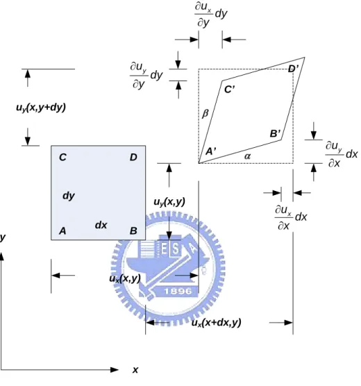
Strain – The application of stress to a body in equilibrium causes it to undergo
deformation or strain. It is the geometrical measure of deformation representing the relative displacement between particles in the material body. Normal strain is defined as the amount of stretch or compression along a material line element while shear strain is a degree of distortion associated with the sliding of plane layers over each other within a deforming body.
Consider a two-dimensional deformation of an infinitesimal rectangular material element with dimensions as shown in Fig. 2.2. From the geometry, we can write
2 2 ' ' ux uy A B dx dx dx x x ∂ ⎛ ⎞ ∂ ⎛ ⎞ = ⎜ + ⎟ + ⎜ ⎟ ∂ ∂ ⎝ ⎠ ⎝ ⎠ (2.7)
Under the assumption of small displacement, which means ∇u<<1, the length of A B' ' can reduce dx+ ∂
(
ux /∂x dx)
. The normal strain in x - direction of the element is defined as' ' x xx u A B AB x AB ε = − ≈∂ ∂ (2.8)
The shear strain is the change of the angle between two originally orthogonal axes. For small rotation (i.e. α, β <<1) and infinitesimal approximation, we get
tan , tan x y y x x x u u dy dx u u y x u x u y dx dx dy dy x y α α β β ∂ ∂ ∂ ∂ ∂ ∂ ≈ = ∂ ≈ ≈ = ∂ ≈ ∂ ∂ + + ∂ ∂ (2.9)
Thus, the shear strain can be written as
y x xy yx u u x y γ = + =α β ∂ +∂ =γ ∂ ∂ (2.10)
By expanding this definition in three dimensions, the strain can be related to the displacements by the following strain components:
11 1 1 1 , 2 2 2 1 1 1 , 2 2 2 1 1 1 , 2 2 2 ε ε ε γ γ ε ε ε γ γ ε ε ε γ γ ⎛ ⎞ ∂ ∂ ∂ = = = ⎜ + ⎟= = ∂ ⎝∂ ∂ ⎠ ⎛ ⎞ ∂ ∂ ∂ = = = ⎜ + ⎟= = ∂ ⎝∂ ∂ ⎠ ∂ ⎛∂ ∂ ⎞ = = = ⎜ + ⎟= = ∂ ⎝∂ ∂ ⎠ xx xy yx xy yx yy yz zy yz zy zz xz zx zx xz u u v x y x v v w y z y w u w z z x (2.11)
where u, v, and w are the displacements in the x, y, and z directions, respectively. The results analogous to those of stress theory hold, and therefore the symmetric array of strain tensor (εkl)
can be arranged as:
xx xy xz kl yx yy yz zx zy zz ε ε ε ε ε ε ε ε ε ε ⎡ ⎤ ⎢ ⎥ = ⎢ ⎥ ⎢ ⎥ ⎣ ⎦ (2.12)
Similar to stress, only six independent components are required to then define the state of strain at a certain point:
T
xx yy zz xy yz zx
ε = ⎣⎡ε ε ε ε ε ε ⎤⎦ (2.13)
2.1.2 Stress-Strain Relationship
The relationship between the stress tensor and the deformation is known as a constitutive relation. All structural materials possess the property of elasticity. When the force is removed, the body will return to its original shape if it is an ideal elastic body and it had not reached its yield stress. For an elastic solid, the stress tensor is linearly proportional to the strain tensor over a specific range of deformation:
σij =cijkl klε (2.14) where cijkl is the tensor of stiffness constants. In order to relate each of the nine elements of
the second rank strain tensor to each of the nine elements of the second rank stress tensor, cijkl
12
the stress and strain tensors under equilibrium, cijkl can reduce a tensor of 36 elements. Crystal
silicon has diamond cubic crystal geometry resulting from its strong directional covalent bonds. For such crystals, cijkl has the following form due to their cubic symmetry:
11 12 12 12 11 12 12 12 11 44 44 44 0 0 0 0 0 0 0 0 0 0 0 0 0 0 0 0 0 0 0 0 0 0 0 0 ijkl c c c c c c c c c c c c c ⎡ ⎤ ⎢ ⎥ ⎢ ⎥ ⎢ ⎥ = ⎢ ⎥ ⎢ ⎥ ⎢ ⎥ ⎢ ⎥ ⎢ ⎥ ⎣ ⎦ (2.15)
Thus, for silicon the tensor of elastic stiffness constants reduces to the three independent components: c11, c12, and c44. Of practical interest is the strain arising from a certain stress
condition. The strain components can be obtained by inverting Hook's law and utilizing the compliance coefficients,
ij sijkl kl
ε = σ (2.16)
The stiffness and compliance tensors are linked through the above relation. Consequently, the three independent compliance coefficients can be calculated as [2.3],[2.4]
11 12 11 2 2 11 11 12 12 12 12 2 2 11 11 12 12 44 44 1 c c s c c c c c s c c c c s c + = + − = + − = (2.17)
The compliance coefficients for Si, together with the stiffness coefficients, are listed in Table 2.1 [2.5].
13
The effect of stress on the resistivity of Si was first investigated by Smith [2.6]. This finding was contributed to the modification of the electronic band structure. Microscopically, stress breaks the symmetry of lattice which can then cause the energy shift and band distortion. In the following these effects are discussed in detail.
Deformation potential theory originally developed by Bardeen and Shockley [2.7] was used to investigate the interaction of electrons with acoustic phonons. It was later generalized to include different scattering modes by Herring and Vogt [2.8]. The technique was applied to strained systems by Bir and Pikus [2.9].
Within the framework of this theory, the energy shift of a band extremum l is expanded in terms of the components of the strain tensor εij.
( )l ( )l ij ij ij
E ε
Δ =
∑
Ξ (2.18)The coefficients of this expansion are called the deformation potential tensor. This tensor is characteristic of a given non-degenerate band in the solid. The symmetry of the strain tensor is also reflected in that of the deformation potential tensor, giving
( )l ( )l ij ji
Ξ = Ξ (2.19) The maximum number of independent components of this tensor is six which can reduce two or three for a cubic lattice. They are usually denoted by Ξu, the uniaxial deformation potential
constant, and Ξd, the dilatation deformation potential constant. The deformation potential
constants can be calculated using theoretical techniques such as density functional theory [2.10], the non-local empirical pseudo-potential method [2.11], or ab-initio calculations. However, a final adjustment of the potentials is obtained only after comparing the calculated values with those obtained from measurement techniques [2.12]–[2.14]. The deformation potential constants used in this work are listed in Table 2.1 [2.15].
14
The general form of the strain-induced energy shifts of the conduction band valleys for an arbitrary strain tensor can be written as
( )i j, ( )j
( )
( )j TC d u i i
E Tr ε a ε a
Δ = Ξ + Ξ ⋅ ⋅ (2.20)
where ai is a unit vector of the ith valley minimum for the jth valley type. The first term in Eq.
(2.20) shifts the energy level of all the valleys equally and is proportional to the hydrostatic strain. The difference in the energy levels of the valleys arises from the second term in Eq. (2.20). In this method, strain effect only shifts the band edge while it does not cause the band warping. In this study, the stress along <110> direction on (001) surface can first be transformed into strain. Then, by applying Eq. (2.20), the quantities of band shift for Δ2 and Δ4 valley can be expressed as
2 4 , 11 12 12 11 , 11 12 12 11 ( )( 2 ) ( )( ) 3 3 ( )( 2 ) ( )( ) 3 6 σ σ σ σ Δ Δ Ξ Ξ Δ = Ξ + + + − Ξ Ξ Δ = Ξ + + − − u u c d u u c d E S S S S E S S S S (2.21)
It is noteworthy that the approximation is reasonable under moderate stress [2.16] while it may need to include the effect band warping for large stress because of the strong influence of effective mass change.
15
References
[2.1] A. P. Boresi, R. J. Schmidt, and O. M. Sidebottom, “Advanced mechanics of
materials,” 5th ed., New York: John Wiley & Son, 1993.
[2.2] H. A. Rueda, “Modeling of mechanical stress in silicon isolation technology and its influence on device characteristics,” Ph.D. Dissertation, University of Florida, 1999.
[2.3] C. Kittel, “Introduction to solid state physics,” 7th ed., New York: John Wiley & Son, 1995.
[2.4] S. Dhar, “Analytical mobility modeling for strained Silicon-based devices” Ph.D. Dissertation, Vienna University of Technology, 2007.
[2.5] Y. Kanda, “Effect of stress on Germanium and Silicon p-n junctions,” Jpn. J. Appl.
Phys., Vol. 6, No. 4, pp. 475-486, 1967.
[2.6] C. S. Smith, “Piezoresistance effect in Germanium and Silicon,” Phys. Rev., vol. 94, no. 1, pp. 42-49, Apr. 1954.
[2.7] J. Bardeen and W. Shockley, “Deformation potentials and mobilities in non-polar crystals,” Phys. Rev., vol. 80, pp. 72-80, Oct. 1950.
[2.8] C. Herring and E. Vogt, “Transport and deformation-potential theory for many-valley semiconductors with anisotropic scattering,” Phys. Rev., vol. 101, pp. 944-961, Feb. 1956.
[2.9] G. L. Bir and G. E. Pikus, “Symmetry and strain induced effects in semiconductors,'' New York: Wiley, 1974.
[2.10] C. G. Van de Walle, “Theoretical calculations of heterojunction discontinuities in the Si/Ge system,” Phys. Rev. B, vol. 34, pp. 5621-5633, Oct. 1986.
16
mobility in strained Si, Ge, and SiGe alloys,” J. Appl. Phys., vol. 80, pp. 2234-2252, Aug. 1996.
[2.12] C. Herring and E. Vogt, “Transport and deformation-potential theory for many-valley semiconductors with anisotropic scattering,” Phys. Rev., vol. 101, pp. 944–961, Feb. 1956.
[2.13] I. Balslev, “Influence of uniaxial stress on the indirect absorption edge in silicon and germanium,” Phys. Rev., vol. 143, pp. 636–647, Mar. 1966.
[2.14] C. G. Van de Walle and R. M. Martin, “Theoretical calculations of heterojunction discontinuities in the Si/Ge system,” Phys. Rev. B, vol. 34, pp. 5621–5634, Oct. 1986.
[2.15] J. S. Lim, S. E. Thompson, and J. G. Fossum, “Comparison of threshold-voltage shifts for uniaxial and biaxial tensile-stressed n-MOSFETs,” IEEE Electron Device
Lett., vol. 25, pp. 731–733, Nov. 2004.
[2.16] Y. Sun, S. E. Thompson, and T. Nishida, “Physics of strain effects in semiconductors and metal-oxide-semiconductor field-effect transistors,” J. Appl. Phys., vol. 101, p. 104503, May 2007.
17
Table 2.1 Compliance and stiffness coefficients, Luttinger parameters, deformation potential constants, and split-off energy for silicon.
Stiffness Coefficients c11 (1012dyne/cm2) 1.657 c12 (1012dyne/cm2) 0.639 c44 (1012dyne/cm2) 0.796 Compliance Coefficients s11 (10-12m2/Nt) 7.68 s12 (10-12m2/Nt) -2.14 s44 (10-12m2/Nt) 12.6
Deformation Potential Constants
Ξd (eV) 1.13
18 A FN FS F (a) y z x yy zz xx yx zy xz zx yz xy (b)
Fig. 2.1 (a) Schematic of an arbitrary force ΔF acting on an infinitesimal area ΔA, along with
the resolved components: normal ΔFN and shear terms ΔFS. (b) A cubic element located
19 ux(x,y) uy(x,y) ux(x+dx,y) uy(x,y+dy) A dx dy D C B D’ C’ B’ A’ ∂ ∂ x u dx x ∂ ∂ y u dx x ∂ ∂ y u dy y ∂ ∂ x u dy y x y
20
Chapter 3
Measurement of Channel Stress Using Gate Direct
Tunneling Current in Uniaxially Stressed
n-MOSFETs
3.1 Introduction
It is well recognized that the mechanical stress in MOSFETs can significantly affect many electrical properties such as the mobility [3.1]–[3.3], the hot carrier immunity [3.4], the threshold voltage [3.5], and the gate direct tunneling current [3.6]–[3.8]. Thus, the ability to quantitatively determine the magnitude of the underlying mechanical stress, as well as its status (compressive or tensile), is essential. Three fundamentally different methods have been introduced in this direction: (i) wafer bending jig [3.9]; (ii) sophisticated stress simulation [3.10]; and (iii) Raman spectroscopy [3.11]. Obviously, the electrical approach to the mechanical stress was lacking to date. However, it is noteworthy that the gate direct tunneling current has been well studied under externally applied mechanical stress [3.6]–[3.8]. Particularly in the citation [3.8], the deformation potential constants [3.12]–[3.14] have been experimentally determined with the values consistent with theoretical works [3.15]. Therefore, with known deformation potential constants, it is plausible to measure mechanical stress by means of the gate direct tunneling current.
In this chapter, we show how to transform the gate direct tunneling current in stressed devices into the value of the stress, achieved without adjusting any parameters. Confirmative evidence is presented in terms of the piezoresistance coefficient electrically created on the
21
same device.
3.2 Experiment
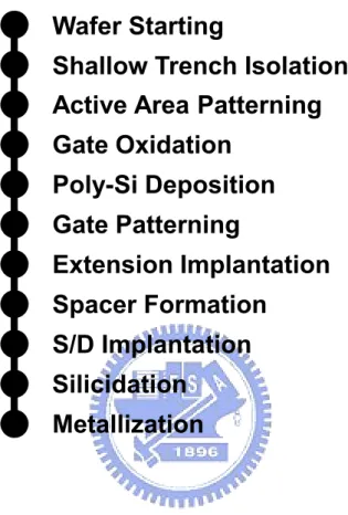
The n+ poly-silicon gate n-MOSFETs were fabricated in a state-of-the-art manufacturing process. The device process flow is depicted in Fig. 3.1. Also plotted in the Fig. 3.2 are the schematic cross section and topside view of the test device. Three key process parameters were obtained by capacitance-voltage (C−V) fitting: n+ poly-silicon doping concentration = 1 × 10 20 cm-3, gate oxide thickness = 1.27 nm, and substrate doping concentration = 4 × 10 17 cm-3. In this process, the STI induced compressive stress was applied. The gate length along the <110> direction is 1 μm large enough that the following effects can be effectively eliminated: external series resistance and short channel or drain induced barrier lowering (DIBL). The gate width is wide (10 μm), indicating that the transverse stress is relatively negligible. Layout technique was utilized to produce a variety of stress in terms of the gate edge to STI sidewall spacing, designated a, with four values of 10, 2.4, 0.495, and 0.21 μm. A decrease in a means increased magnitude of longitudinal stress. A considerable number of contacts were formed on the source/drain diffusion along the gate width direction, far away from the STI in the <110> direction. The spacing between the diffusion contact and the gate edge is fixed in this work. It has been reported that silicide can introduce stress into channel and its effect can be eliminated by well controlling the silicide formation [3.10]. Thus, the silicide process was fine tuned for the device under study to minimize its effect as compared with STI stress.
The gate direct tunneling current was measured in inversion conditions with the source, drain, and substrate all tied to ground. Also characterized was the mobility on the same device at Vd = 25 mV. The change of the conduction-band electron direct tunneling current at Vg = 1
22
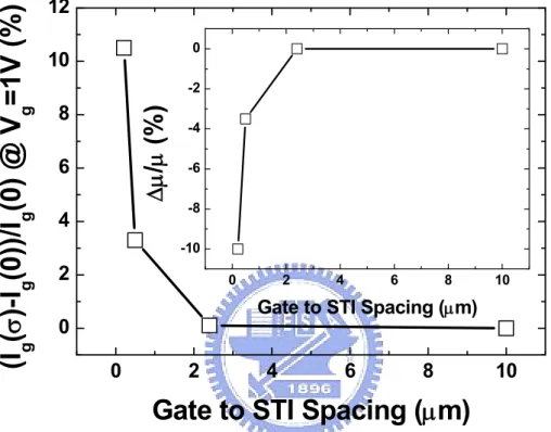
V and the mobility at Vg = 0.5 V, all with respect to a = 10 μm, are plotted in Fig. 3.3 versus
gate to STI spacing. It can be seen that a decrease in the gate to STI spacing can produce an increase in both the gate current while degrading the mobility.
3.3 Stress Extraction
Existing direct tunneling models [3.16], [3.17] on the basis of the triangular potential approximation [3.18] in the channel, taking into account the poly-silicon depletion, can readily apply with some slight modifications such as incorporating stress dependencies of the subbands. The electrons in inversion primarily populate the two lowest subbands [3.8]: one of the two-fold valley Δ2 and one of the four-fold valley Δ4. The corresponding stress dependencies are well defined in the literature [3.8], [3.12]–[3.14]:
2 , 2 3 2 * 11 12 12 11 2 9 ( ) ( ) ( )( 2 ) ( )( ) 3 3 16 2 eff u u d hqE E S S S S m σ Δ σ σ Δ Δ Ξ Ξ = + Ξ + + + − (3.1) 2 , 4 3 4 * 11 12 12 11 4 9 ( ) ( ) ( )( 2 ) ( )( ) 3 6 16 2 eff u u d hqE E S S S S m σ Δ σ σ Δ Δ Ξ Ξ = + Ξ + + − − (3.2)
where the quantization effective masses m*Δ2 = 0.92 m0 and m*Δ4 = 0.19 m0; and the elastic
compliance constants S11 = 7.68 × 10⁻¹² m2 /N and S12 = −2.14 × 10⁻¹² m2/N. The hydrostatic and shear deformation potential constants Ξd = 1.13 eV and Ξu = 9.16 eV [3.5], close to those
of Ref. [3.8], were cited here. Stress along <110> direction can be resolved into two different components: normal and shear stress terms in <100> coordination. Shear terms can cause the band distortion, which in turn, influences the effective mass. This effect becomes significant when applied strain approaches 1% and beyond, whose magnitude is much greater than that in our study case. Thus, it is reasonable to assume that effective mass change can be neglected under moderate stress in the subsequent calculation. One of the expressions for the effective
23
electric field Eeff can be found elsewhere [3.8]. With the aforementioned process parameters as
input, the two lowest subband levels with respect to the Fermi level Ef can be determined. The
stress dependencies of the lowest subbands under different gate voltages were found to be consistent with those in earlier works [3.8]. The inversion-layer carrier density per unit area
can further be calculated by ( / 2) ln(1 exp(( ) / ))
i B i di f i B
N = k T πh g m + E −E k T [3.16]–[3.18],
where the subscript i denotes Δ2 or Δ4, kBT is the thermal energy, gi is the degeneracy of the
valley, and mdi is the density of state effective mass. It is then a straightforward task to
calculate the WKB tunneling probability, taking into account the corrections for reflections from the potential discontinuities [3.19]. Here the electron effective mass in the oxide for the parabolic type dispersion relationship was used with mox ~ 0.50 m0, which is equivalent to mox
= 0.61 m0 for the tunneling electrons in the oxide using the Franz type dispersion relationship
[3.20]. The oxide can be thought of as an amorphous material. The irregular arrangement of oxide atoms makes its band structure and the electron tunneling effective mass in this layer difficult to be determined, especially for the strain condition. The theoretical calculation or experimental extraction of tunneling mass considering stress effect was still lacking. Thus, in this work, we assume that the electron effective mass in the oxide remains unchanged with stress varying. This assumption works well in predicting the strain-induced gate tunneling current [3.8]. The SiO2/Si interface barrier height in the absence of stress is 3.15 eV. Consequently, without adjusting any parameters, the conduction-band electron direct tunneling current density can be calculated as a function of the stress σ [3.8]:
2 4 2 4 ( ) ( ) ( ) ( ) ( ) g qN qN I σ σ σ τ σΔΔ τ σΔΔ = + (3.3) The tunneling lifetime in Eq.(3.3) can be related to the transmission probability T: τΔ2(σ) =
πħ/(TΔ2(σ)EΔ2(σ)) and τΔ4(σ) = πħ/(TΔ4(σ)EΔ4(σ)).
24
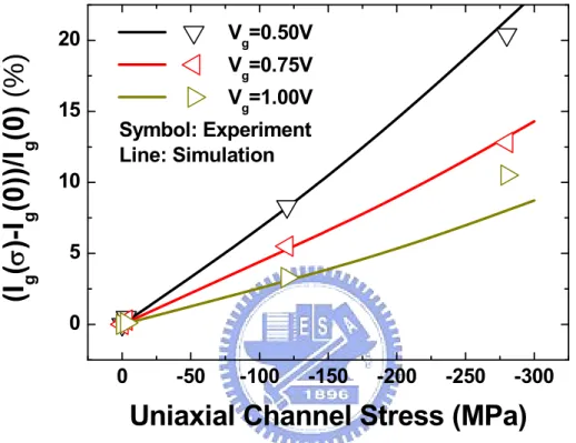
and -280 MPa for gate to STI spacing of 10, 2.4, 0.495, and 0.21 μm, respectively, can reproduce gate direct tunneling current versus gate voltage characteristics. The corresponding gate current change is plotted in Fig. 3.4 versus extracted channel stress with gate voltage as a parameter. It can be seen that the magnitude of the gate current change increases linearly with the stress, consistent with those published elsewhere [3.8]. Again in agreement with the citation [3.8], the slope of the straight line in Fig. 3.4 increases with decreasing gate voltage. This trend also points out that the accuracy of the proposed method can be considerably improved by lowering gate voltages.
3.4 Confirmative Evidence
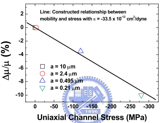
The measured mobility change percentage versus extracted stress is shown in Fig. 3.5. The straight line through the data points yields the slope or piezoresistance coefficient of -33.5 × 10 -12 dyne-1 cm2, close to that (-31.5 × 10 -12 dyne-1 cm2) in the literature [3.21].
To testify to the layout technique mentioned above, we quote existing relationship between the effective channel stress and the gate to STI spacing, which was derived from the stress simulation [3.10]: ( ) ( )(1 min) min a a a V a a =σ + mσ − σ (3.4)
where amin represents a minimum gate to STI spacing and Vm is the maximum σ(a) variations (i.e. when a → ∞) with respect to σ(amin). The extracted stress can be adequately described by Eq. (3.4) with Vmσ = -1.05, as demonstrated in Fig. 3.6. Indeed, the projected stress for a = 10 μm, the reference point mentioned above, approaches zero. Therefore, the layout technique holds true in this work.
25
other devices (with a sample size of 10) on the same wafer. The corresponding stress-induced variations in gate direct tunneling current were found to be comparable with those in Fig. 3.4.
3.5 Conclusion
With known process parameters and published deformation potential constants as input, fitting of gate direct tunneling current versus gate voltage data has led to the value of the underlying channel stress. A link with the mobility measurement on the same device has been conducted. The resulting piezoresistance coefficient has been in good agreement with literature values. The layout technique has also been validated.
26
References
[3.1] J. Welser, J. L. Hoyt, and J. F. Gibbons, “NMOS and PMOS transistors fabricated in strained silicon/relaxed silicon-germanium structures,” in IEDM Tech. Dig., 1992, pp. 1000–1002.
[3.2] S. E. Thompson, M. Armstrong, C. Auth, M. Alavi, M. Buehler, R. Chau, S. Cea, T. Ghani, G. Glass, T. Hoffman, C. H. Jan, C. Kenyon, J. Klaus, K. Kuhn, Z. Ma, B. Mcintyre, K. Mistry, A. Murthy, B. Obradovic, R. Nagisetty, P. Nguyen, S. Sivakumar, R. Shaheed, L. Shifren, B. Tufts, S. Tyagi, M. Bohr, and Y. El-Mansy, “A 90-nm logic technology featuring strained-silicon,” IEEE Trans. Electron
Devices, vol. 51, pp. 1790–1797, Nov. 2004.
[3.3] C. H. Ge, C. C. Lin, C. H. Ko, C. C. Huang, Y. C. Huang, B. W. Chan, B. C. Perng, C. C. Sheu, P. Y. Tsai, L. G. Yao, C. L. Wu, T. L. Lee, C. J. Chen, C. T. Wang, S. C. Lin, Y. C. Yeo, and C. Hu, “Process-strained Si (PSS) CMOS technology featuring 3D strain engineering,” in IEDM Tech. Dig., 2003, pp. 73–76.
[3.4] A. Hamada, T. Furusawa, N. Saito, and E. Takeda, “A new aspect of mechanical stress effects in scaled MOS devices,” IEEE Trans. Electron Devices, vol. 38, pp. 895–900, Apr. 1991.
[3.5] J. S. Lim, S. E. Thompson, and J. G. Fossum, “Comparison of threshold-voltage shifts for uniaxial and biaxial tensile-stressed n-MOSFETs,” IEEE Electron Device
Lett., vol. 25, pp. 731–733, Nov. 2004.
[3.6] W. Zhao, A. Seabaugh, V. Adams, D. Jovanovic, and B. Winstead, “Opposing
dependence of the electron and hole gate currents in SOI MOSFETs under uniaxial strain,” IEEE Electron Device Lett., vol. 26, pp. 410–412, Jun. 2005.
27
[3.7] X. Yang, J. Lim, G. Sun, K. Wu, T. Nishida, and S. E. Thompson, “Strain-induced changes in the gate tunneling currents in p-channel metal–oxide–semiconductor field-effect transistors,” Appl. Phys. Lett., vol. 88, pp. 052108, Jan. 2006.
[3.8] J. S. Lim, X. Yang, T. Nishida, and S. E. Thompson, “Measurement of conduction band deformation potential constants using gate direct tunneling current in n-type metal oxide semiconductor field effect transistors under mechanical stress,” Appl.
Phys. Lett., vol. 89, pp. 073509, Aug. 2006.
[3.9] C. Gallon, G. Reimbold, G. Ghibaudo, R. A. Bianchi, R. Gwoziecki, S. Orain, E. Robilliart, C. Raynaud, and H. Dansas, “Electrical analysis of mechanical stress induced by STI in short MOSFETs using externally applied stress,” IEEE Trans.
Electron Devices, vol. 51, pp. 1254–1261, Aug. 2004.
[3.10] R. A. Bianchi, G. Bouche, and O. Roux-dit-Buisson, “Accurate modeling of trench isolation induced mechanical stress effects on MOSFET electrical performance,” in
IEDM Tech. Dig., 2002, pp. 117–120.
[3.11] I. D. Wolf, “Micro-Raman spectroscopy to study local mechanical stress in silicon integrated circuits,” Semicond. Sci. Technol., vol. 11, pp. 139–154, 1996.
[3.12] C. Herring and E. Vogt, “Transport and deformation-potential theory for many-valley semiconductors with anisotropic scattering,” Phys. Rev., vol. 101, pp. 944–961, Feb. 1956.
[3.13] I. Balslev, “Influence of uniaxial stress on the indirect absorption edge in silicon and germanium,” Phys. Rev., vol. 143, pp. 636–647, Mar. 1966.
[3.14] C. G. Van de Walle and R. M. Martin, “Theoretical calculations of heterojunction discontinuities in the Si/Ge system,” Phys. Rev. B, vol. 34, pp. 5621–5634, Oct. 1986.
28
[3.15] M. V. Fischetti and S. E. Laux, “Band structure, deformation potentials, and carrier mobility in strained Si, Ge, and SiGe alloys,” J. Appl. Phys., vol. 80, pp. 2234–2252, Aug. 1996.
[3.16] N. Yang, W. K. Henson, J. R. Hauser, and J. J. Wortman, “Modeling study of ultrathin gate oxides using direct tunneling current and capacitance-voltage measurements in MOS devices,” IEEE Trans. Electron Devices, vol. 46, pp. 1464–1471, Jul. 1999.
[3.17] K. N. Yang, H. T. Huang, M. C. Chang, C. M. Chu, Y. S. Chen, M. J. Chen, Y. M. Lin, M. C. Yu, S. M. Jang, C. H. Yu, and M. S. Liang, “A physical model for hole direct tunneling current in p+ poly-gate pMOSFETs with ultrathin gate oxides,” IEEE
Trans. Electron Devices, vol. 47, pp. 2161–2166, Nov. 2000.
[3.18] H. H. Mueller and M. J. Schulz, “Simplified method to calculate the band bending and the subband energies in MOS capacitors,” IEEE Trans. Electron Devices, vol. 44, pp. 1539–1543, Sep. 1997.
[3.19] L. F. Register, E. Rosenbaum, and K. Yang, “Analytic model for direct tunneling current in polycrystalline silicon-gate metal-oxide-semiconductor devices,” Appl.
Phys. Lett., vol. 74, pp. 457–459, Jan. 1999.
[3.20] Z. A. Weinberg, “On tunneling in metal-oxide-silicon structures,” J. Appl. Phys., vol. 53, pp. 5052–5056, Jul. 1982.
[3.21] S. Suthram, J. C. Ziegert, T. Nishida, and S. E. Thompson, “Piezoresistance coefficients of (100) silicon nMOSFETs measured at low and high (~1.5 GPa) channel stress,” IEEE Electron Device Lett., vol. 28, pp. 58–61, Jan. 2007.
29
Wafer Starting
Shallow Trench Isolation
Active Area Patterning
Gate Oxidation
Poly-Si Deposition
Gate Patterning
Extension Implantation
Spacer Formation
S/D Implantation
Silicidation
Metallization
30
Compressive
stress
Gate
STI
STI
a
a
Compressive
stress
Gate
STI
STI
a
a
Compressive
stress
Gate
STI
STI
a
a
(a)STI Stress STI Stress
a
a
STI Stress STI Stress
a
a
(b)
Fig. 3.2 (a) Schematic cross section and (b) topside view of the device under study. The gate edge to STI sidewall, a, is highlighted. The stress condition is compressive due to the lower thermal expansion rate of STI oxide compared to silicon.
31 0 2 4 6 8 10 0 2 4 6 8 10 12
(I
g(
σ
)-I
g(0))/I
g(0) @ V
g=1V
(%)
Gate to STI Spacing (
μ
m)
Fig. 3.3 The relative change of the gate direct tunneling current at Vg = 1V versus gate to STI
spacing. The inset shows the mobility variations versus the gate to STI spacing.
0 2 4 6 8 10 -10 -8 -6 -4 -2 0
Δμ
/
μ
(%
)
32 0 -50 -100 -150 -200 -250 -300 0 5 10 15 20
(I
g(
σ
)-I
g(0))/I
g(0)
(%)
Uniaxial Channel Stress (MPa)
Vg=0.50V Vg=0.75V Vg=1.00V Symbol: Experiment Line: Simulation
Fig. 3.4 The relative change of the gate direct tunneling current versus extracted uniaxial compressive channel stress for Vg = 0.5, 0.75, and 1V. The symbols are experimental data.
33 0 -50 -100 -150 -200 -250 -300 -10 -8 -6 -4 -2 0
2 Line: Constructed relationship between
mobility and stress with π = -33.5 x 10⁻¹² cm2/dyne
a = 10 μm a = 2.4 μm a = 0.495 μm a = 0.21 μm
Δμ/μ
(%
)
Uniaxial Channel Stress (MPa)
Fig. 3.5 The measured mobility change versus extracted stress. Fitting the data yields the value of piezoresistance coefficient π = -33.5 × 10 -12 dyne-1 cm2.
34 0 2 4 6 8 10 0.0 0.2 0.4 0.6 0.8 1.0 Channel Stress Symbols: Experiment Lines: Model fitting
σ
(a)/
σ
(a
min)
Gate to STI Spacing (
μ
m)
Fig. 3.6 The extracted stress, divided by that of the minimum a, versus the gate to STI spacing, along with a fitting curve from Eq. (3.4).
35
Chapter 4
Distinguishing Between STI Stress and Delta Width
in Gate Direct Tunneling Current of Narrow
n-MOSFETs
4.1. Introduction
The significance of the shallow trench isolation (STI) induced mechanical stress in highly scaled MOSFETs has been widely recognized [4.1]. The linkage between layout design and the underlying STI stress has also been well constructed [4.2]-[4.4]. Further applications pertaining to the layout dependencies of the STI stress altered dopant diffusion [4.5],[4.6], gate direct tunneling [4.6],[4.7], threshold voltage [4.6]-[4.8], subthreshold leakage [4.6],[4.8], and mobility [4.2],[4.4],[4.6],[4.7], have all been successfully demonstrated. However, care must be taken especially in the narrowing direction. The reasons are that on the one hand, the STI channel stress can be enhanced; however, on the other hand, the delta width ΔW due to
STI corner rounding as schematically shown in Fig. 4.1 is of increasing importance. Thus, the ability to distinguish the delta width effect from the STI stress effect is essential. Two such examples on the drain current variation have recently been published [4.9],[4.10]. However, so far, effects on the gate direct tunneling current counterpart were not yet addressed in the open literature. In this work, we elaborate on how to unambiguously elucidate the STI stress altered gate direct tunneling current measured in the presence of n-MOSFET narrowing.
36
4.2 Experiment
The n+ poly-silicon gate n-MOSFETs on (001) wafer were fabricated in a state-of-the-art manufacturing process. Three key process parameters were obtained by a capacitance-voltage (C−V) fitting: n+ poly-silicon doping concentration = 1 × 10 20 cm-3, gate oxide thickness = 1.27 nm, and channel doping concentration = 3 × 10 17 cm-3. In this process, STI induced compressive stress was applied. The gate length L, the gate edge to STI spacing in source diffusion, and the gate edge to STI spacing in drain diffusion, all in the channel length direction <110>, were fixed at the same value of 0.5 μm. The gate edge to STI spacing in the source diffusion is equal to that of the drain: The cross-sectional view of the test device is schematically shown in Fig. 4.1. The gate width W spanned in a wide range of 0.11, 0.24, 0.6, 1.0 and 10 μm. The gate direct tunneling current was measured in inversion with the source, drain, and substrate all tied to the ground. The change percentage of the apparent gate current per unit width, namely the actual gate current divided by corresponding W, with respect to W = 10 μm, is plotted in Fig. 4.2 for Vg = 1 V versus W.
4.3 Data Fitting and Parameter Extraction
As illustrated in Fig. 4.1, the actual channel width designated Weff is the drawn gate width
plus the delta width: Weff = W + ΔW. The corresponding stress altered gate tunneling current
density can be expressed as a linear function of both the average longitudinal channel stress
σx and the average transverse channel stress σy , which was obtained via a triangular potential
based quantum simulation while incorporating the longitudinal and transverse stress dependencies of the subbands [4.11]:
![Fig. 4.1 The cross-sectional view of the device in the channel width direction, which can be schematically drawn from the existing simulated device structure in a state-of-the-art manufacturing process [4.3]](https://thumb-ap.123doks.com/thumbv2/9libinfo/8476840.183786/58.892.222.672.258.726/sectional-direction-schematically-existing-simulated-structure-manufacturing-process.webp)
