國 立 交 通 大 學
電子工程學系 電子研究所碩士班
碩 士 論 文
抑制癲癇發作的雙極性刺激器以及
抑制癲癇發作的雙極性刺激器以及
抑制癲癇發作的雙極性刺激器以及
抑制癲癇發作的雙極性刺激器以及
在低電壓製程下負高壓產生器設計
在低電壓製程下負高壓產生器設計
在低電壓製程下負高壓產生器設計
在低電壓製程下負高壓產生器設計
Design of Biphasic Stimulus Driver to Suppress
Epileptic Seizure and Negative High Voltage
Generator in the Low Voltage Process
研 究 生: 黃雅君 (Ya-Chun Huang)
指導教授: 柯明道教授 (Prof. Ming-Dou Ker)
中華民國一○一年九月
抑制癲癇發作的雙極性刺激器以及
抑制癲癇發作的雙極性刺激器以及
抑制癲癇發作的雙極性刺激器以及
抑制癲癇發作的雙極性刺激器以及
在低電壓製程下負高壓產生器設計
在低電壓製程下負高壓產生器設計
在低電壓製程下負高壓產生器設計
在低電壓製程下負高壓產生器設計
Design of Biphasic Stimulus Driver to Suppress Epileptic
Seizure and Negative High Voltage Generator in the Low
Voltage Process
研 究 生:黃雅君
Student: Ya-Chun Huang
指導教授:柯明道教授
Advisor: Prof. Ming-Dou Ker
國立交通大學
電子工程學系
電子研究所
碩士論文
A Thesis
Submitted to Department of Electronics Engineering and
Institute of Electronics
College of Electrical and Computer Engineering
National Chiao Tung University
in Partial Fulfillment of the Requirements
for the Degree of
Master of Science
in
Electronics Engineering
September 2012
Hsinchu, Taiwan
中華民國一○一年九月
抑制癲癇發作的雙極性刺激器以及
抑制癲癇發作的雙極性刺激器以及
抑制癲癇發作的雙極性刺激器以及
抑制癲癇發作的雙極性刺激器以及
在低電壓製程下負高壓產生器設計
在低電壓製程下負高壓產生器設計
在低電壓製程下負高壓產生器設計
在低電壓製程下負高壓產生器設計
學生: 黃 雅 君 指導教授: 柯 明 道 教授
國立交通大學
電子工程學系 電子研究所碩士班
摘要
摘要
摘要
摘要
在臨床醫學上,生醫晶片的推動改變了多數醫療方法,也解決很多以往 不能解決的疾病,例如植入視網膜晶片,使盲人重見光明。廣義來說,結合 微電子技術、醫學以及生物化學,可以製造應用不同疾病醫療之生物晶片, 例如癲癇晶片。 抑制癲癇的方法為輸出定電流抑制,然而電極植入不同大鼠腦組織之等 效阻抗皆不同,必須做刺激器電路針對不同大鼠樣本皆能產生定電流週期性 脈波輸出。在刺激器刺激下,需要一個相對應的反向電流使腦內電荷平衡,避免電極的氧化還原電荷影響人體。刺激方式分為兩種:兩根針(雙極性)刺激 以及一根針(單極性)刺激。雙極性刺激為輸出高低電位之兩根電極做刺激,其 高低電位會互換,使電流周期性地正負反向;單極性刺激為一根電極對地做 刺激,當輸出刺激電流時電極輸出電壓為正電壓,反向電流時電極電壓為負 電壓。 在具有雙極性刺激的癲癇晶片內,輸出級需要 4~10V 的高電壓,又系統 晶片之供應電壓只有 1.8V,必須建立直流-直流變壓器將 1.8V 升到 4~10V 之 高壓以供應不同阻抗行電刺激。在此研究中提出在低電壓製程下實現負載適 應性之變化,並內嵌入有效變頻可調式高壓產生器,一來降低電壓轉換率, 使電極上電流不易發生突波;二來,在電極植入不深之情況下,在兩電極不 同間距時可以有較低功耗。本刺激器可支援雙極性及單極性刺激,並加入數 位類比轉換器調整輸出電流之大小以供動物實驗用。本次雙極性刺激器可選 擇輸出電流 20µA, 30µA 和 40µA,在刺激的電流 30µA 下可刺激的電極阻抗 之電容值在 4nF 到 200nF、10kΩ 到 250kΩ,並在 TSMC 0.18µm 1.8V/3.3V 低 電壓製程下實現。 在生醫晶片單極性刺激下,需要一個負高壓產生器(~-8V)供給刺激器負電 壓,而設計一個在低電壓製程不會造成閘極可靠度問題且無閂鎖效應之負高 壓產生器是一件具有挑戰性的事情。本負高壓產生器可穩在-8V,其輸出電流 可高達 320µA,在負載電流 200 µA 時功率轉換率為 42.26%,電源電壓調整 率為 0.166V/V,負載調整率為 0.194mV/µA。
Design of Biphasic Stimulus Driver to Suppress
Epileptic Seizure and Negative High Voltage
Generator in the Low Voltage Process
Student: Ya-Chun Huang
Advisor: Prof. Ming-Dou Ker
Department of Electronics Engineering & Institute of Electronics
National Chiao-Tung University
Abstract
Nowadays, the clinical therapy changes since the emerging of the biomedical chips. In addition, more diseases could be cured thanks to the invention, e.g. the artificial retina. By extension, the biomedical chip is made by the combination of microelectronics, medicine and biochemical such as epilepsy prosthetic SoC.
The methodology to suppress epilepsy seizure is constant current stimulation. However, there are different values of electrode-tissue impedance through different kinds of electrode and sample rat. The stimulus driver must provide the constant
periodic current pulses to different rats and electrodes. For avoiding the electrochemical process to damage the tissue, the reversed current pulses which amplitude is equal to the stimulus current is required after stimulating. The stimulation methodology is divided into two types: two leads per site (bipolar stimulation) and one lead per site (monopolar stimulation). For bipolar stimulation, two electrodes supply high and low voltage to the tissue respectively. The voltage levels of two electrodes exchange periodically so that the stimulus current flowing through the tissue becomes positive or negative alternately. For monopolar stimulation, one electrode supplies the adaptive voltage to the ground. When stimulating, the electrode provides positive voltage to generate the positive stimulus current. After stimulating, the electrode provides negative voltage to generate the negative reversed current.
In epilepsy prosthetic SoC, the high voltage potential 4~10V is required in the output stage. However, the power supply of the SoC is only 1.8V. DC-DC boost converter should be required to raise the voltage potential for the stimulus driver. In the report, we introduce the stimulus driver with loading adaptive consideration in the low-voltage process. Besides, the positive high voltage generator with effective PFM controller is embedded within the stimulus driver to control the switching speed and dynamic power effectively. First, it reduces the slew rate to free from the glitch current on the electrode. Second, when stimulating, it consumes lower power within the electrode implanted shallower (low capacitance). The stimulus driver supports monopolar and bipolar stimulation. In addition, with DAC applied, the output stimulus current could be 20µA, 30µA and 40µA within the electrode-tissue impedance from 4nF to 200nF and from 20kΩ to 250kΩ at stimulus current 30µA in the TSMC 0.18µm 1.8V/3.3V general purpose process.
In monopolar stimulation of biomedical chips, the negative high voltage generator (~-8V) is needed. With the potential for mass production, CMOS technologies are more attractive to realize the system on a chip (SoC). Therefore, the positive and negative high voltage generators should be feasible in the commercial low-voltage CMOS processes. The proposed negative high voltage generator could be regulated at -8V. The maximum output current is up to 320µA. When the output current is 200µA, the power efficiency is 42.26%. The line regulation is 0.166V/V. The load regulation is 0.194mV/µA.
Contents
摘要 摘要 摘要 摘要 ... iii Abstract ... v Acknowledgment ... x List of Tables ... xiList of Figures ... xii
Chapter 1 Introduction ... 1
1.1 Motivation ... 1
1.2 Thesis Organization ... 3
Chapter 2 Background of Epilepsy, Stimulus Driver and Epilepsy SoC Development ... 4
2.1 Overview of Epilepsy and Epileptic Treatment ... 4
2.2 Brief Inroduction ... 8
2.2.1 Introduction of Treatment ... 8
2.2.2 Epileptic Seizure Detecting and Controlling System ... 12
2.2.3 Brief Introduction of Implantable Stimulus Driver ... 13
2.3 Introduction of Epilepsy SoC Development ... 18
Chapter 3 Design of Biphasic Stimulus Driver to Suppress Epileptic Seizure with Adaptive Loading Consideration ... 20
3.1 Introduction ... 20
3.2 Impedance Analysis ... 21
3.3 Design of Biphasic Stimulus Driver ... 26
3.3.1 Implementation ... 26
3.3.2 VCC Generator ... 30
3.3.3 Sensing Circuit and Output Driver ... 34
3.3.4 Simulation and Measurement Results ... 37
3.3.5 Animal Test ... 48
3.4 Summary ... 52
Chapter 4 Negative High Voltage Generator ... 53
4.1 Introduction ... 53
4.2 Proposed Negative High Voltage Generator ... 55
4.2.2 4-Phase Clock Generator and Tapped Buffer ... 57
4.2.3 Compartor ... 58
4.2.4 PFM Feedback ... 59
4.2.5 ESD Consideration for Negative Voltage Generator in Low Voltage Process ... 60
4.3 Simulation Results and Measurement Results ... 61
4.4 Summary ... 70
Chapter 5 Conclusions and Future Works ... 71
5.1 Conclusions ... 71
5.1.1 Biphasic Stimulus Driver... 71
5.1.2 Negative High Voltage Generator ... 72
5.2 Future Works ... 72
5.2.1 Monopolar Stimulation ... 72
5.2.2 Advanced Animal Test ... 73
5.2.3 Stimulus Driver on Humans ... 73
References ... 76
Vita ... 80
Acknowledgment
感謝柯明道老師在這兩年的教導,讓我學到了非常多的東西,不僅僅是在於 學理上的精進,更學到了許多人生中的道理。也要感謝交大眾多教授的指教,每 一堂課都對我的研究有很大的助益。 還有實驗室的同伴們,陳仲君、吳佳王民、林宥婕、戴嘉岑、蔡翔宇、郭品 宏、范鐏元、周家維、鄭銘幓、劉耀嘉,學習的過程中一同扶持與成長,能與大 家一起渡過的這段時間,將會是我一生中美好回憶之一。以及實驗室的學長姐, 林群祐學長、顏承正學長、陸亭州學長、邱柏硯學長、黃世豪學長、王資閔學長、 葉致廷學長、艾菲學長、竹立煒學長、翁怡歆學姊、蔡惠雯學姐、林倍如學姐、 黃文杰學長、陳旻毅學長、張堂龍學長、陳偉霖學長、歐陽有儀學長、周敬呈學 長、莊書瑾學姊、彭子薰學長、黃建軒學長、何明翰學長、陳思翰學長、林佑達 學長、李易儒學長、黃筱晴學姐、黃瑀晴學妹、顧珊綺學妹、林冠宇學弟。還有 爸爸媽媽給予經濟上的支援,之前實習華邦電子前輩給予的經驗(感謝馬爺等 人),CIC 和工研院給的 shuttle 機會,更要感謝交大土地公保庇讓晶片能動且成 績可以順利 pass。 最後再次感謝爸爸媽媽以及永遠的朋友西苑幫,精神喊話之「媽~我一定會賺 大錢讓你住豪宅做貴婦」,還有謝謝蔡蟲、炸機、米血兒、山菜、貴婦、gay 髮、 熊熊、鳳梨…等 30 人精神永在的義氣相挺。 論文雖然力求完善,但謬誤之處在所難免,尚祈各位讀者不吝惜賜予寶貴意 見,使本論文能更加完善。List of Tables
Table 3.1. Table for correspondence between digital signal and the target current.
... 36
Table 3.2. Comparison specification, pre-simulation, post-simulation and measurement results. ... 47
Table 3.3. Table for the impedance adaptive range. ... 47
Table 4.1. SCR specification in this work. ... 60
Table 4.2. Comparison of specification, pre-layout simulation, post-layout simulation and measurement results. ... 63
Table 4.3. Simulation Results of the comparator. ... 64
Table 4.4. Simulation results of LDO. ... 65
List of Figures
Fig. 2.01. Lobes of the brain [9]. ... 6 Fig. 2.02. 3Hz spike and wave activity. Absence epilepsy and primary generalized
epilepsy. ... 6 Fig. 2.03. Different frontal gyri and functional gyrus within the frontal lobe. Three gyri on the lateral surface of the frontal lobe are F1,F2 and F3. ... 7 Fig. 2.04. Doctor implants the clinic electrode to the brain to detect the long-term
EEG, investigate the area of seizure occurrence and evaluate the side effect after surgery. ... 9 Fig. 2.05. Clinical electrodes are implanted to investigate the electroencephalogram
(EEG) brain wave[13]. ... 10 Fig. 2.06. Four methods of stimulation: (a) transcranial magnetic stimulation
(TMS), (b) deep brain stimulation (DBS), (c) vagus nerve stimulation (VNS) and (d) neurosurgery for mental disorders (NMD) [15]. ... 11 Fig. 2.07. The closed-loop epileptic seizure monitor and controller [21]. ... 13 Fig. 2.08. Different stimulation method affects the components in the stimulus
driver. ... 15 Fig. 2.09. Biphasic waveform when stimulating. ... 15 Fig. 2.10. Biphasic waveform with one-lead per site [24]. ... 16 Fig. 2.11. Biphasic Wave with two-leads (bipolar stimulation): (a) circuit model of
bipolar stimulus driver (b) circuit model for electrode and tissue surface and (c) bipolar sitmulator circuit[25]. ... 17 Fig. 2.12. Epileptic SoC block diagram. ... 19 Fig. 3.01. Equivalent circuit of the tissue-brain impedance [25]. ... 22 Fig. 3.02. (a) Impedance amplitude of different rat samples(ZI-2,ZI-3, ZI-4 and
ZI-5) and time(ZI-5-1 and ZI-5-2) plot versus frequency; (b) phase plot of different rat samples(ZI-2,ZI-3, ZI-4 and ZI-5) and time(ZI-5-1 and ZI-5-2) plot versus frequency. ... 23 Fig. 3.03. (a) Impedance amplitude of different rat samples(ZI-2,ZI-3, ZI-4 and
ZI-5) and time(ZI-5-1 and ZI-5-2) plot versus frequency; (b) phase plot of different rat samples(ZI-2,ZI-3, ZI-4 and ZI-5) and time(ZI-5-1 and ZI-5-2) plot versus frequency. ... 24 Fig. 3.04. Tissue impedance of experiment results with long-term investigation
verses implanted time in different stimulus site (ZI) [26]. ... 25 Fig. 3.05. The proposed stimulus driver consists of output stage with VCC
generator, sensing circuit, and output driver. ... 27 Fig. 3.06. The operation of stimulus driver for biphasic current pulse. ... 27 Fig. 3.07. The brief block diagram is illustrated diagram for the stimulus driver. 28 Fig. 3.08. The waveforms of the important nodes as the resistance is big and the
capacitance is small. ... 29 Fig. 3.09. VCC generator with 5-stage charge pump, tapped buffer, 2-phase clock
generator, proposed PFM block, comparator, ring oscillator and
frequency divider. ... 30 Fig. 3.10. (a) Five-stage charge pump with gate-oxide reliability in the low-voltage
process[28]. (b) The SC circuit represents charge pump. Dynamic power is related to frequency. ... 31 Fig. 3.11. Charge pump controlling signal circuit block (a) 32MHz ring oscillator.
(b) Frequency divider with Johnson counter and the binary counter. (c) Non-overlapping clock generator for MHz clock. ... 32 Fig. 3.12. The proposed PFM block. ... 33 Fig. 3.13. Sensing circuit and sensing condition. ... 35 Fig. 3.14. (a) High-tolerant output driver and (b) Trimming for tuning stimulus
current for different rats. ... 36 Fig. 3.15. Die photograph of the new proposed biphasic stimulus driver. ... 38 Fig. 3.16. The measurement setup of devices. The outputs of stimulus driver are
connects to test board with the electrode equivalent circuit. ... 38 Fig. 3.17. Measured frequency: (a) ring oscillator : 28.08MHz (b) the frequency
divider combining Johnson counter and binary counter : 2.83MHz. ... 39 Fig. 3.18. The comparison of the measured operating electrode voltages VL1 and
VL2 between big C (C=200nF) and small C(C=4nF). ... 40 Fig. 3.19. The comparison of the measured electrode voltages VL1 between big C
(C=200nF) and small C(C=4nF). ... 40 Fig. 3.20. The comparison of the measured electrode voltages VL1 between
different loading resistance R=200kΩ and R=290kΩ. ... 41
Fig. 3.21. The measurement result of stimulus current between electrode resistance R=200kΩ and R=290kΩ when electrode capacitance is 4nF and the digital signal abc is 110. ... 41 Fig. 3.22. The measurement result of stimulus current between electrode resistance
R=200kΩ and R=290kΩ when electrode capacitance is 200nF and the digital signal abc is 110. ... 42 Fig. 3.23. The measurement results of stimulus currents with electrode resistance
from 10 kΩ to 473 kΩ when electrode capacitance is 4nF. As abc is 111, the target current is 20uA. As abc is 110, the target current is 30uA. As
abc is 100, the target current is 40uA. ... 43 Fig. 3.24. The measurement results of stimulus currents with electrode resistance
from 10 kΩ to 473 kΩ when electrode capacitance is 4nF. As abc is 111, the target current is 20uA. As abc is 110, the target current is 30uA. As abc is 100, the target current is 40uA. ... 43 Fig. 3.25. The measurement results of current mismatch between Icathodic and
Ianodic with electrode resistance from 10 kΩ to 473 kΩ when electrode capacitance is 4nF. As abc is 111, the target current is 20uA. As abc is 110, the target current is 30uA. As abc is 100, the target current is 40uA. .... 44 Fig. 3.26. The measurement results of current mismatch between Icathodic and
Ianodic with electrode resistance from 10 kΩ to 473 kΩ when electrode capacitance is 200nF As abc is 111, the target current is 20uA. As abc is 110, the target current is 30uA. As abc is 100, the target current is 40uA. ... 44 Fig. 3.27. The measurement results of VCC generator with electrode resistance
from 10 kΩ to 473 kΩ when electrode capacitance is 200nF. As abc is 111, the target current is 20uA. As abc is 110, the target current is 30uA. As abc is 100, the target current is 40uA. ... 45 Fig. 3.28. The measurement results of power consumption (a) when the electrode
capacitance is 4nF (b) when the electrode capacitance is 200nF. As abc is 111, the target current is 20uA. As abc is 110, the target current is 30uA. As abc is 100, the target current is 40uA. ... 46 Fig. 3.29. The measurement setup of integration experiment of proposed stimulus
driver and closed-loop epileptic seizure monitoring system. ... 48 Fig. 3.30. The redesign PCB where die is bonded is used to do animal experiment.
Biphasic input signals are used and the stimulus driver provides the stimulus current. ... 49 Fig. 3.31. The EEG wave recorded: (a) normal condition (b) seizure without
suppression within 11s (two measured times). ... 50 Fig. 3.32. The experiment result with natural seizure. Epilepsy seizure with
abnormal discharge happens. As detecting the seizure, the stimulus current is delivered to the brain. The seizure suppression costs
approximately 1s by 800Hz and duty cycle 10% pulses. ... 51 Fig. 3.33. The experiment result with natural seizure. As detecting the seizure, the
stimulus current is delivered to the brain. The seizure suppression costs approximately 4s by 800Hz and duty cycle 40% pulses. ... 51 Fig. 4.01. Biphasic stimulator for electrical stimulation. ... 54 Fig. 4.02. Conventional negative high voltage generator with PMOS switches. ... 54
Fig. 4.03. Design of the negative high voltage generator. ... 56
Fig. 4.04. 6-stage all deep N-well NMOS negative charge pump... 57
Fig. 4.05. Clock diagram for pumping signals. ... 57
Fig. 4.06. The 4-phase clock generator. ... 58
Fig. 4.07. (a) Block diagram and (b) schematic diagram of comparator design. .... 59
Fig. 4.08. The cross-section view and ESD path of the SCR which is used in the proposed negative voltage generator. ... 60
Fig. 4.09. Prelayout-simulation of the comparator with SS 125℃℃℃℃, TT 25℃℃℃ and FF ℃ -40℃℃℃℃. OP gain almost larger than 55dB ,bandwidth larger than 100MHz and PM >45∘∘∘∘. ... 64
Fig. 4.10. Post-layout simulation of the comparator with SS 125℃℃℃, TT 25℃℃ ℃℃ and ℃ FF -40℃℃℃℃. OP gain almost larger than 55dB ,bandwidth larger than 150MHz and PM >45∘∘∘. ... 65∘
Fig. 4.11. Die photograph with A: 4-phase clock generator, B: tapped buffer, C: 6-stage negative charge pump, D: comparator, E: PFM feedback, and F: loading capacitor. ... 66
Fig. 4.12. Measurement setup of the proposed negative high voltage generator. ... 66
Fig. 4.13. The measured output voltage (Vss) versus the loading current tested by different clock frequencies. ... 67
Fig. 4.14. The measured output voltage (Vss) versus the power supply (VDD) tested by different clock frequencies. ... 67
Fig. 4.15. The power efficiency versus clock frequency under loading resistor 40k Ω Ω Ω Ω. ... 68
Fig. 4.16. The power efficiency versus clock frequency under loading resistor 25k Ω Ω Ω Ω. ... 68
Fig. 4.17. The power efficiency versus loading current. ... 69
Fig. 5.01. The block diagram of monopolar stimulation. ... 73
Fig. 5.02. The electrode implanted on humans (a) the electrodes with PCB to connect the impedance analyzer Agilent 4294A. (b) the electrode diagram. ... 74
Fig. 5.03. (a) Electrode capacitance distribution. Most electrode capacitances are 100~120nF. (b) Electrode resistance distribution. Most electrode resistances are 60~70kΩ. ... 75
Chapter 1
Introduction
1.1 Motivation
Bioelectronics emerges for the evolution and promotion of biomedical science and electronic engineering. As a result, some new therapies are proposed through the advanced technology. Several applications, such as resonance imaging, are launched and helpful to patients and doctors in the surgery. Neuroscience which is one of biomedical science is the main accordance for the proposed application called neuromuscular electrical stimulation or functional electrical stimulation (FES) in general. FES is the application of electrical current to excitable tissue to complement or substitute for function that is lost in neurologically injured organization, as usually the case with spinal cord injury (SCI) [1]. Epilepsy is neurological diseases and FES could be applied to this case.
Epilepsy is the second common neurological disorder, affecting 50 million people all over the world. 25% of patients with epilepsy have seizures which couldn’t be controlled by drug or surgery. Neurological diseases mean the disorder of the nerve system and cause the paralysis of the signal transmission between nerve cells. Therapies of epileptic seizure include pharmacologic treatment and surgical treatment, pharmacologic treatment since medical science becomes improved. However, not all patients could afford surgery because this is risky surgery that might cause functional losses. In fact, in these patients, only 75% do response well to traditional therapies [2]. The incidence rates of epileptic seizures and epileptic seizures with centre-temporal (Ro-landic) discharges were found to be 134/100,000 and 21/100,000, respectively.
These were determined in an epidemiological study in a population consisting of 52,252 children aged 0–15 years in a county in the northern part of Sweden. Epileptic seizures with Rolandic discharges represented about 16% of all the epileptic seizures (febrile convulsions not included) [3]. Nowadays, epilepsy becomes predictable by analyzing EEG in the frequency domains, several methods of prediction have been researched, including predictable features and prediction by classification [4], [5]. It also has been demonstrated that the abnormal discharge signal that causes epilepsy can be suppressed by FES when detecting the abnormal brain wave [6]. It is feasible to those patients who couldn’t take surgical treatment.
Although FES is a feasible method to suppress epileptic seizure, there are several challenges in designing the stimulus driver shown as follows. (1) Due to different rat samples, kinds of electrodes, location, and implanted time, effective impedance of electrode will varies in a wide range. The impedance ranges from tens of kΩ to several hundreds of kΩ. Under the condition, while required stimulus current is fixed, output voltage varies in a wide range correspondingly. (2) For SoC integration, high operating voltage results in problems of gate-oxide overstress, hot-carrier effect, and other reliability issues in the low-voltage process [7]. (3) Power consumption is the critical consideration. The more power consumption is, the less the utility time of the implantable device is. (4) Latch-up issue: for semiconductor, the latch-up is easy to occur when transferring the negative voltage or the high voltage in the system is higher than the breakdown voltage of the lateral pn-junction. This thesis proposes two circuits applied to the biomedical chip. One is the negative high voltage generator; the other is the operation-voltage-generated stimulus driver with consideration of adaptive loading in wider range fabricated in the low-voltage process. Two circuits are verified on silicon with measurement results.
1.2 Thesis Organization
This chapter includes the motivation of this work and the thesis organization. The chapter 2 of this thesis introduces some background knowledge of epilepsy, epileptic seizures treatment, and implantable stimulus driver.
In the chapter 3, design of negative high voltage generator for monopolar stimulation is proposed, which has been verified in the 0.18-µm 1.8-V/3.3-V general purpose process for SoC integration. The negative high voltage generator free from gate-oxide overstress and latch-up and efficiency-enhanced compared with the prior art.
In the chapter 4, design of biphaic stimulus driver to suppress epileptic seizure with current-mode adaptive loading consideration is proposed. The stimulus driver comprises of two block circuit – the voltage generator and the driver. The voltage generator is included to supply the adaptive operating voltage to the electrode. The driver connected to the electrode should be high reliability for fear the gate-oxide overstress.
The last chapter, chapter 5, recapitulates the major consideration of this thesis and concludes with suggestions for future investigation.
Chapter 2
Background of Epilepsy, Stimulus Driver and
Epilepsy SoC Development
2.1 Overview of Epilepsy and Epileptic Treatment
Epilepsy, caused by excessive abnormal discharge in the brain and represented by constant seizures, is a neurological disorder [8]. This is the brain disease. Doctors implant the electrodes to watch the brain wave and judge whether epilepsy seizure the patient gets. As for the brain, there are five lobes and Amygdala shown in Fig. 2.01. Some of them are the reason for causing epileptic seizure. Epilepsy is divided into five types:
(1) Absence Epilepsy
Patients with absence epilepsy are almost children. The reason of the syndrome is considered to be related to inheritance from parents. Absence seizures are broadly categorized into typical and atypical absence seizures. Typical epilepsy seizures occur in the context of idiopathic generalised epilepsies and EEG shows faster than 3 Hz generalised spike-wave discharges shown in Fig. 2.02, approximately 7-12Hz. Otherwise( slower than 3Hz spike), epilepsy seizures are atypical [9]. When absence epilepsy attacks, patients space out throughout the day no matter whether someone call them or wake up them.
(2) Frontal Lobe Epilepsy
Epilepsy caused by the damage in the frontal lobe is named frontal lobe epilepsy. Frontal lobe, the largest part of the lobes of the brain shown in Fig. 2.01, is the second most common lobe in which epilepsy surgery is performed. Three gyrus of frontal lobe are inferior frontal gyrus, precentral gyrus and medial frontal gyrus shown in Fig. 2.03. Precentral gyrus is the primary motor area. During surgery, this area could be stimulated with current. The movements that result from stimulating this area are movements of the limbs, hands, and face [9].
(3) Temporal Lobe Epilepsy
Temporal lobe, the most heterogeneous of the lobes and frequent cause of epilepsy, controls the function of language, hearing and memory. Injury on temporal lobe results in partial seizures and aura. Furthermore, it is hard to take a surgery to cut off for fear the loss of functions.
(4) Occipital Lobe Epilepsy
Damage to occipital causes a homonymous hemianopsia, which is bilateral loss of vision [9]. During a seizure, excessive activity could result in both positive phenomenon such as flashing lights, or a negative phenomenon like black spots.
(5) Parietal Lobe Epilepsy
The parietal lobe, between the frontal and temporal lobes, is the primary sensory area. When stimulating this area, pain is never experienced but removal of this area results in function devastating. Parietal lobe seizures tend to spread to other areas of the brain.
Fig. 2.01. Lobes of the brain [9].
Fig. 2.03. Different frontal gyri and functional gyrus within the frontal lobe. Three gyri on the lateral surface of the frontal lobe are F1,F2 and F3.
2.2 Brief Inroduction
2.2.1 Introduction of Treatment
There are two treatments shown as follows: (1) surgical treatment and (2) pharmacologic treatment.
Surgical treatment is a high-risk option for patients whose seizures cannot be controlled with medications [10]. Because all epilepsy seizures occur in the lobes which control different function, such as hearing, language and memory for temporal lobe, surgery for cutting the seizure area may lose function. Besides, there is no guarantee that epileptic seizures can be cured exactly. Before the surgery, doctors would implant the clinical electrode to determine where the seizure occurs in the brain and which function may be lost if taking surgery shown in Fig. 2.04. Epilepsy evaluation includes the investigations such as long-term EEG recording (most and shown in Fig. 2.05), neurological examination, MRI, etc. What kind of surgery is applied depends on different kind of seizures and the location of the brain. There are two basic brain surgeries for epilepsy, resection surgery and disconnection surgery. The most common type of resection surgery is temporal lobectomy. In latter type, sometime called functional disconnection, surgeon interrupts the nerve direction that spread abnormal discharges. However, surgical treatment is not a suitable option because some sections of brain are too important to remove. For example, removal of temporal lobe might results in the malfunction of hearing, language and memory function.
Pharmacologic treatment is basic and the most used therapy. According to patient’s condition, and what kind of epilepsy, doctors choose suitable medications (antiepileptic drugs or AED) for treatment. There are two types of AEDs used, narrow
spectrum AEDs focus on small number of epileptic seizures, and broad spectrum AEDs work for a large group of seizures. However, epilepsy is a complicated disease. No standard recipe which medication to use for epileptic patient could be decided. The effectiveness and side effects are mainly consideration of prescription. Most of patients’ condition can be ameliorated by AEDs, however, every kind of medicines sometimes might lead to side effects including blurry vision, dizziness, headaches, and fatigue [11], [12]. In addition, these medications might lead to allergic in roughly 10% of people and can impair blood cell or liver. Unfortunately, some patients do not respond to AEDs, their epilepsy is medically refractory. They might take other treatments into consideration such as surgical treatment.
Fig. 2.04. Doctor implants the clinic electrode to the brain to detect the long-term EEG, investigate the area of seizure occurrence and evaluate the side effect after surgery.
Fig. 2.05. Clinical electrodes are implanted to investigate the electroencephalogram (EEG) brain wave[13].
Except for pharmacologic treatment and surgical treatment, electrical stimulation is a treatment for drug-resistant epilepsy and has been investigated [14]. Advantages of electrical stimulation are flexible, recoverable, and non-destructive. Four methods of stimulation are feasible as follows: (1) transcranial magnetic stimulation (TMS), (2) deep brain stimulation (DBS), (3) vagus nerve stimulation (VNS) and (4)neurosurgery for mental disorders (NMD) as shown in Fig. 2.04 [15]. TMS is a relatively safe procedure as it does not involve any surgery or require general anaesthesia. The few risks that are associated with its use are determined largely by the number, intensity and frequency of stimuli applied. TMS and ppTMS at low frequency are unlikely to produce seizures, or have any lasting effects on cognition, but rTMS, by increasing cortical excitability, can precipitate seizures even in healthy subjects [16].The vagus nerve is autonomic nervous system, which controls body functions that are not under voluntary control. The vagus nerve is situated the neck and connect abdomen and the lower part of brain. Device of VNS consists of pulse generator, flexible wire, and electrodes. By sending regular pulses of electrical signal via vagus nerve, VNS system
can suppresses epileptic seizures before seizures happen. Currently, VNS is approved by Food and Drug Administration (FDA). DBS is emerging as an important treatment in the management of PD and other movement disorders. The application of DBS involves delivering a current using implanted quadripolar electrodes connected to a battery powered pulse-generating device. as shown in Fig. 2.06(b) [15]. Our epilepsy stimulus driver is based on deep brain stimulation (DBS).
Fig. 2.06. Four methods of stimulation: (a) transcranial magnetic stimulation (TMS), (b) deep brain stimulation (DBS), (c) vagus nerve stimulation (VNS) and (d) neurosurgery for mental disorders (NMD) [15].
2.2.2 Epileptic Seizure Detecting and Controlling System
Recently, EEG is used to record the brain wave and process this signal to detect the epilepsy seizure [17], [18]. It also has been demonstrated that the abnormal discharge signal that causes epilepsy can be suppressed by FES before epileptic seizures happen [16]. A variety of epileptic seizure detecting and controlling systems has been studied and implemented. The systems for epileptic treatment are mainly classified by stimulus types, open-loop systems and closed-loop systems [19].
Open-loop systems, or so called blind systems, do not respond to physiological activity immediately. The neuroscientists intend to modulate seizures by activating and inactivating region and set the required stimulus current for individual. Open-loop systems regularly turn on and off at a fixed pattern which is determined by neuroscientists before the event. Currently existing systems that approved by FDA are all adopts open-loop systems [16]. Closed-loop systems, so called intelligent systems, are more complicated. The systems are switched on by detecting seizures onset. In comparison with open-loop systems, closed-loop systems can minimize the effect to human body. Closed-loop systems consist of detector, signal analyzer, and stimulus driver. As current researches shown, epileptic seizures could be tracked back to tens of seconds before onset. For example, closed-loop system may be quite effective for epileptic seizure in the hippocampus, where seizures may remain confined for up to 10 seconds prior to propagation [20]. Therefore, a number of algorithms have been proposed for rapidly detecting and classifying the sign of different kind of epileptic seizures. These algorithms analyze the brain activities records from EEG or electrocorticogram (ECOG) and extract the feature of seizure-like brainwave, and the outcome of analysis can be utilized to switch on therapeutic intervention. Due to
complexity of closed-loop systems, power consumption is one of mainly considerations of embedded systems. Fig. 2.06 is a closed-loop epileptic seizure monitor and controller presented in 2009 [21].
Fig. 2.07. The closed-loop epileptic seizure monitor and controller [21].
2.2.3 Brief Introduction of Implantable Stimulus Driver
Functional electrical stimulation (FES) has been developed and implemented for different kinds of applications in biomedical science and clinical therapies [1]. Some diseases were considered hard to cure in the past, such as the retinitis pigmentosa (RP) [2], Alzheimer’s disease [23], and damaged central nervous system. Nowadays, these diseases might become curable through implantable stimulus driver. Therefore, a variety of implantable stimulus drivers have been researched and presented. Based on FES, the stimulation wave combines cathodic wave with anodic wave alternatively. That is, the biphasic waveform is needed. Besides, the method of stimulation is divided into two types: (1) two interface leads per site (bipolar stimulation) and (2) one interface lead per site (monopolar stimulation) shown as Fig. 2.08(a) [22]. For one interface lead per site (monopolar stimulation), we need the positive and negative high voltage sources respectively. For two interface leads per site (bipolar stimulation), the positive high voltage source is required. Moreover, the way of stimulation affects the complexity of the circuit.
run away from electrodes into tissue. In other words, free electrons in the electrodes oxidize through the faradaic reaction and cause the charge imbalance in the tissue. Therefore, the biphasic waveform is required for charge balance .In epileptic SoC, the biphasic stimulus current is applied.
The prior art of the monopolar stimulation is shown in Fig. 2.10 [24]. This work is used in the epiretinal prosthesis chip. The positive high voltage regulator +12V and negative high voltage regulator -12V provide the electrode voltage. With current mismatch problem, the charge cancellation circuit is added to let the charges on the electrodes release to ground. DAC is used to control the amplitude of the output current. At the output stage, the high voltage(32V) MOSFETs are used to afford 12V voltage so that it could avoid the semiconductor issue such as hot-carriers or punch-through. The output resistance is equal to one resistor Relec series one capacitor
Celec with Relec=10kΩ and Celec=100nF. The circuit would realize with additional mask
for SoC integration.
Fig. 2.11 indicates the stimulus driver in the bipolar stimulation [25]. This work is also applied in retinal prosthesis. Using 0.35 µm HV CMOS process with 20V power supply, the current mismatch achieves less than 0.4µA smaller than the work in [24]. There are three phases: cathodic phase, anodic phase and shorting phase. In the cathodic phase, S1 is close to deliver charge to WE, while anodic to cancel delivered
charge. Using shorting alone to achieve charge balance may cause unwanted neural response to neighboring sites. The output resistance is shown in Fig. 2.11(b) with CE=100nF, RF=10MΩ and RT=9kΩ. Fig. 2.11(c) shows the stimulus circuit.
MHP2,MHP3,MHN2 and MHN3 are switches which gives the biphasic current into
electrode. The current source driver has large output impedance to bias the electrode adaptive operating voltage in RT=9kΩ. Using active cascade current source is that
Fig. 2.08. Different stimulation method affects the components in the stimulus driver.
Fig. 2.11. Biphasic Wave with two-leads per site (bipolar stimulation): (a) circuit model of bipolar stimulus driver (b) circuit model for electrode and tissue surface and (c) bipolar sitmulator circuit [25].
2.3 Introduction of Epilepsy SoC Development
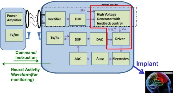
In the epileptic SoC architecture, the SoC circuit block is shown in Fig. 2.12. The system is called close-loop system. Two routes for the close-loop system: (1) sensing route and (2) writing route. For sensing route, pre-amplifier reads the EEG signals from electrodes. Pre-amplifier provides the tunable gain and bandwidth. Next, ADC digitalizes the analog signals into digital signals to DSP system. DSP system uses CRC computation to generate the TX signals. TX circuits deliver the encoding EEG signals to the monitor outside to investigate the brain wave and detect the epileptic seizure. Also, the epileptic seizure detector is embedded into implantable DSP system. After detecting, if there is a seizure, DSP would give an enable signal to the stimulus driver to supply periodic constant current pulse which frequency is 800Hz.
Before, the voltage of output stage must be higher enough to drive the load and the high voltage supply is constant. In this work, the high voltage power of the stimulus driver is tunable depending on the loading impedance. No matter loading impedance is, the high voltage generator would output the adaptive voltage to provide the electrode with constant current pulse. For this changeable high voltage power, it can stimulus different rats and save power. In other words, the stimulus driver would provide the electrode voltage with loading adaptive consideration.
Chapter 3
Design of Biphasic Stimulus Driver to Suppress
Epileptic Seizure with Adaptive Loading
Consideration
3.1 Introduction
Nowadays, biomedical chip taken as therapies of some clinical experiments becomes more and more popular. Some biomedical chips such as retinitis pigmentosa (RP) are experimented in the animal to make sure the therapy function and performance.
In the epileptic SoC project, we experiment the proposed stimulus driver on long-evans(rats) which has epilepsy hereditarily. The stimulus current to suppress the seizure of the long-evans is 30µA. However, different rats need different stimulus currents. Therefore, the stimulus current must be tunable to output different current to different rats. The stimulus current would not be too large so that the rat would not feel too hot or hurt. As the stimulus current is too larger, the rat would scream and get hurt.
This stimulus driver is based on functional electrical stimulation (FES). With adaptive current pulses, the epileptic seizure would be suppressed. Furthermore, with reverse current, it would do charge cancellation for fear tissue damage. The proposed stimulus driver includes output driver, current sensing circuit to send digital signal to VCC generator and VCC generator. With VCC generator, it would generate the adaptive voltage for electrode. With wider impedance distribution, the method would
save power for loading consideration since the output voltage of VCC generator is not constant. Using current-mode (current sensing) would calibrate the effect of capacitance of electrodes. Capacitance of the electrode affects the conductance to the tissue. Resistance of the electrode affects the electrode necessary voltage to flow enough current through the tissue.
In this chapter, first we analyze the impedance between the tissue and electrode. Second, the proposed stimulus driver is introduced. Third, the measurement results are presented. Finally, we show the animal test results.
3.2 Impedance Analysis
The equivalent circuit of the electrode-tissue is shown in Fig. 3.01 as for the aspect of resistance and capacitance. Capacitance Cd1 represents the interface between
two materials (metal and meat). Rf represents the faradaic resistance because of
electrochemical process in the electrodes. Rs is the spreading resistance on behalf of the hindrance for the ionic flow. The electrochemical process does not usually appear so that the resistance of dc path from electrode or IC to meat is large. For most stimulus current pulse, it passes through the electrode most. The DC voltage between Cd1 is small enough to neglect the Faradaic effect. That is, Rf is neglected since
Faradaic reaction is seldom when stimulating. The tissue may be polarized because of the capacitance Cd1. Since the faradaic resistance is larger to be neglected, the
measured impedance would transform into the equation in Eq.(3-1). 1 | | j | | cos | | sin Z Z e Z j Z R j C θ
θ
θ
ω
= = + = + (3-1)With DBS(deep brain stimulation), ZI electrode is implanted into the brain of the long-evans with thin metal line 6.5mm~7.2mm(posterior 4.0 mm, lateral 2.5 mm, and
depth 6.5-7.2 mm). Take four rats(ZI-2, ZI-3, ZI-4 and ZI-5) as measurement samples, we measure the impedance of ZI electrode. Furthermore, ZI-5-1 and ZI-5-2 are measured by different time. The time interval is two week. Before measuring the impedance, we first detect whether the two electrode channel could pass the electrical signal. The impedance measurement is shown in Fig. 3.02. There are five curves in the MATLAB impedance plot. That is, different samples have different impedance distribution. Because of the capacitance, the impedance amplitude decreases with frequency shown in Fig. 3.02(a). By Eq.(3-1), the resistance and capacitance are analyzed shown in Fig. 3.03. The resistance of electrode decreases with frequency increasing. The capacitance of electrode decreases with frequency increasing. For the long-term investigation, the impedance changes with time. That is, the resistance of electrode would change continuously shown in Fig. 3.04.
(a)
(b)
Fig. 3.02. (a) Impedance amplitude of different rat samples(ZI-2,ZI-3, ZI-4 and ZI-5) and time(ZI-5-1 and ZI-5-2) plot versus frequency; (b) phase plot of different rat samples(ZI-2,ZI-3, ZI-4 and ZI-5) and time(ZI-5-1 and ZI-5-2) plot versus frequency.
(a)
(b)
Fig. 3.03.(a) Impedance amplitude of different rat samples(ZI-2,ZI-3, ZI-4 and ZI-5) and time(ZI-5-1 and ZI-5-2) plot versus frequency; (b) phase plot of different rat samples(ZI-2,ZI-3, ZI-4 and ZI-5) and time(ZI-5-1 and ZI-5-2) plot versus frequency.
Fig. 3.04. Tissue impedance of experiment results with long-term investigation versus implanted time in different stimulus site (ZI) [26].
3.3 Design of Biphasic Stimulus Driver
From function electrical stimulation (FES) [1], the biphasic current is required to make sure the light injury to the cell. For the wider range of the resistance of the electrode, the loading adaptive consideration is added when designing this work. Since it is medical devices, the reliability and safety are important. In this work, the stimulus driver could self-generate high enough voltage to drive high impedance. Furthermore, the reliability is guaranteed for output driver and VCC generator in the low voltage process so the safety is ensured. Within the range of adaptive resistance and capacitance, the proposed stimulus driver would provide the constant current pulses.
3.3.1 Implementation
The proposed stimulus driver consists of output stage with VCC generator, sensing circuit, and output driver, as shown in Fig. 3.05. In practice, depending on different kind of stimulus sites, therapeutic requirement, and implanted time, tissue impedance varies from tens of kΩ to hundreds of kΩ. The experimental required stimulus current is 30 µA in this work. Under the condition that required seizure suppressing stimulus current is 30 µA, the difference of varying required operating voltage is 4 V. Conventional stimulus devices are used to set the operating voltage at highest requirement and enlarge voltage compliance as large as possible [27]; however, it enlarges power consumption in great amount. That is, output voltage and required power supply are wide spread from low voltage to high voltage. Therefore, the proposed design embedded a VCC generator to generate the appropriate voltage to the electrode. In the output driver, MOSFET must afford the
high voltage up to ~10V. In the low voltage process, if a MOS must afford high voltage, gate-oxide reliability and hot-carrier degradation are noteworthy. Therefore, we have to use stacked MOS to solve these problems.
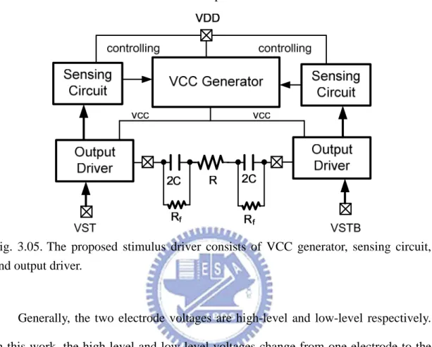
Fig. 3.05. The proposed stimulus driver consists of VCC generator, sensing circuit, and output driver.
Generally, the two electrode voltages are high-level and low-level respectively. In this work, the high-level and low-level voltages change from one electrode to the other alternately. If VST is 1 and VSTB is 0, the stimulus current is produced. If VST is 0 and VSTB is 1, the electrode voltages exchange and the reversed current is generated. If VST is 0 and VSTB is 0, the capacitance in the electrode discharges because of current mismatch.
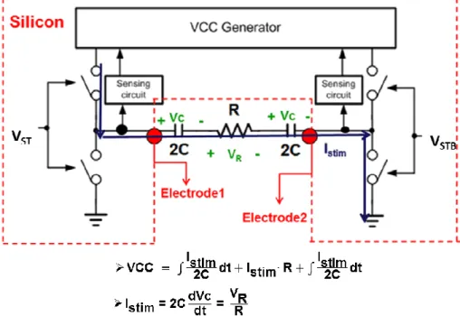
In brief, the proposed stimulus driver system could be illustrated as Fig. 3.06. Assume the two output drivers are ideal switches which no headroom or voltage drop between VCC generator output and electrode. When capacitance of electrodes is small, the voltage of electrode ramps up all the time. When the voltage of electrode is at high level, it increases with time. For providing the electrode adaptive operating voltage, VCC generator would output voltage as Eq. (3-2).
2 2 stim stim stim I I VCC dt I R dt C C =
∫
+ ⋅ +∫
(3-2)
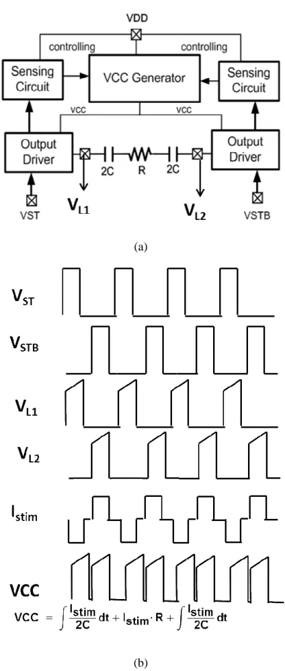
With appropriate controlling signal, VCC generator could be controlled completely by the sensing circuit to generate the adapt electrode voltage shown as Fig. 3.08.
(a)
(b)
Fig. 3.08. The waveforms of the important nodes when the resistance is big and the capacitance is small.
3.3.2 VCC Generator
Fig. 3.09 shows VCC generator with 5-stage charge pump, tapped buffer, 2-phase clock generator, proposed PFM block, comparator, ring oscillator and frequency divider. Because of the wide spread range of power supply, the charge pump must redesign to meet the specification. For the charge pump, the higher the output voltage is, the higher the pumping frequency and the stage number should be. The dynamic power is higher when the pumping frequency is higher for Eq. (3-3).
2
dyn
P
α
CV f(3-3)
There are two properties in designing VCC generator. First, if the slew rate of the electrode voltage is too large, the current glitch would happen. It is easy to see the glitch current when using higher frequency but low dc voltage gain or low feedback speed. Second, as the wider range of the electrode voltage, the output of VCC generator should be variable with adjustable stage number or changeable pumping frequency.
5-stage charge pump
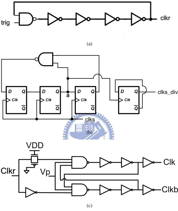
Proposed PFM block 2-phase clock generator Ring Osc ÷ 10 clkr clks clks_div Tapped Buffer clk clkb VDD
Fig. 3.09. VCC generator with a 5-stage charge pump, tapped buffer, 2-phase clock generator, proposed PFM block, comparator, ring oscillator and frequency divider.
Therefore, the proposed PFM block is used to choose the frequency to avoid the high frequency pass through the circuit block with high parasitic capacitance. If the loading resistance is low (the electrode voltage is low), the pumping frequency is not high necessarily. Hence, when the output voltage is low, the proposed PFM block choose the low frequency to pump and recovery. Although recovery time is be larger than that at high frequency, the ripple at low frequency pumping at low electrode voltage is allowed. Second, as the required electrode voltage is low(<5V), the glitch current doesn’t happen anymore once the pumping frequency is not as higher as that used for providing high voltage(9V).
(a)
(b)
Fig. 3.10. (a) Five-stage charge pump with gate-oxide reliability in the low-voltage process [28]. (b) The SC circuit represents charge pump. Dynamic power is related to frequency.
(a)
(b)
(c)
Fig. 3.11. Charge pump controlling signal circuit block (a) 32MHz ring oscillator. (b) Frequency divider with Johnson counter and the binary counter. (c) Non-overlapping clock generator for MHz clock.
Fig. 3.12.The proposed PFM block. Vfb_cp is VCC divided by 5. The frequency of clkr_ori is higher ten times than that of clkr_div. As the electrode needs low voltage, the low pumping frequency is chosen. While the electrode needs high voltage, the high pumping frequency is required.
The way to choose the pumping frequency is based on the value VCC. Fig. 3.12 shows the proposed PFM block. If VCC is smaller than 5V(Vref for VCC generator), the PFM block choose the low frequency clkr_ori to pump and recovery for fear dynamic power. If VCC is larger than 5V, the high frequency clkr_div is chosen.
3.3.3 Sensing Circuit and Output Driver
We use current sensing circuit to provide the digital signal to VCC generator shown in Fig. 3.13. Comparison condition of the sensing circuit is Eq.(3-4)
Vfb =bias1,2−Istim⋅R (3-4) If stimulus current is smaller than the target value, that is the voltage of Vfb is
bigger than Vbg, the output of the comparator is 1. After switch controller, the comparison signal is delivered to the VCC generator and the output voltage of VCC generator increases until the stimulus current achieves the target value.
With the high output voltage of VCC generator, the stimulus driver must be high voltage tolerant. Therefore, the stacked MOS is used to avoid gate-oxide overstress. Suitable gate bias for stacked MOS could avoid hot-carrier degradation. We use level shifters and control circuits to give the adaptive bias to stacked MOS. In addition, adding digital signal could tune the resistor value so that the stimulus current could be tunable.
(a)
(b)
Fig. 3.14. (a) High-tolerant output driver and (b) Trimming for tunable stimulus current for different rats.
Table 3.1 Table for correspondence between digital signal and the target current.
Digital signal(abc)
Target Current I
targetabc=100 40uA
abc=110 30uA
3.3.4 Simulation and Measurement Results
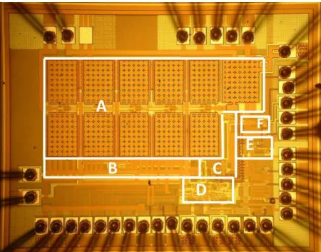
This work is fabricated in TSMC 0.18µm 1.8V/3.3V process with 1.13mmx1.435mm shown in Fig. 3.15, which includes charge pump (A), non-overlapping clock generator (B), effective PFM block (C), output driver and sensing circuit (D), ring oscillator (E), and frequency divider(F).
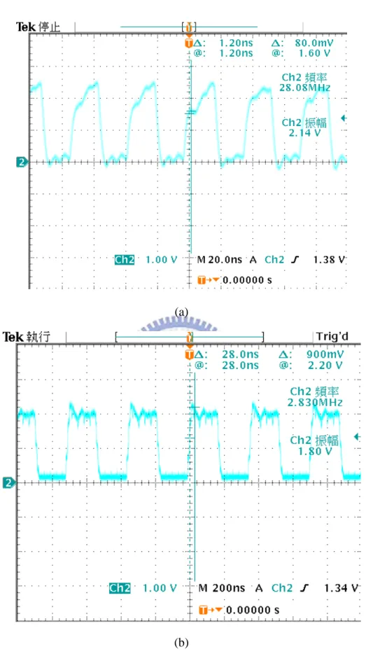
The measurement setup is shown in Fig. 3.16, where Agilent E3631A is utilized to provide the fixed 1.8 V for 1.8-V normal device. Agilent 81110A generates non-overlapping duty cycle 10% 800Hz clock signal for VST and VSTB. TDS 3054B is used to observe output current of the stimulus driver. The first measurement step is measure the ring oscillator and frequency divider. The measured frequencies of the ring oscillator and frequency divider are 28.08MHz and 2.83MHz respectfully shown in Fig. 3.17. These frequency is the choice for the proposed PFM block. As the maximum frequency is 28.08MHz, the maximum output voltage is 9.9V when abc is 100 and output loading resistance is 220kΩ. With different capacitance, the electrode voltage would be different. Fig. 3.18 and Fig 3.19 show the electrode voltages when C is 4nF and C is 200nF. With small capacitance, the electrode voltage increases with time obviously. Fig. 3.20 shows the electrode voltage when R is 200kΩ and 290kΩ. With the resistance difference of 90kΩ, the dc voltage difference is approximately 1.5V. That is, the capacitance affects the change of the electrode voltage with time. The resistance influences the dc voltage of the electrode voltage. Fig. 3.21 shows the comparison of the stimulus currents flowing through R between different C. Fig. 3.22 shows the comparison of the stimulus current waves between different R.
Fig. 3.15. Die photograph of the new proposed biphasic stimulus driver.
Fig. 3.16. The measurement setup of the power supply, the function generator and the oscilloscope. The outputs of stimulus driver connect to test board with the electrode equivalent circuit.
(a)
(b)
Fig. 3.17. Measured frequency: (a) ring oscillator : 28.08MHz (b) the frequency divider combining Johnson counter and binary counter : 2.83MHz.
Fig. 3.18 The comparison of the measured operating electrode voltages VL1 and VL2 between big C (C=200nF) and small C(C=4nF).
Fig. 3.19 The comparison of the measured electrode voltages VL1 between big C (C=200nF) and small C(C=4nF).
Fig. 3.20 The comparison of the measured electrode voltages VL1 between different loading resistance R=200kΩ and R=290 kΩ.
Fig. 3.21 The measurement result of stimulus current between electrode resistance R=200kΩ and R=290kΩ when electrode capacitance is 4nF and the digital signal abc is 110.
Fig. 3.22 The measurement result of stimulus current between electrode resistance R=200kΩ and R=290kΩ when electrode capacitance is 200nF and the digital signal abc is 110.
As the stimulus current tunability, the proposed design would provide the stimulus current 20µA, 30 µA, and 40µA with different digital signals shown in table 3.1. The measurement results are closed to the specification with different loading impedance. For the measurement results shown in Fig. 3.23 and Fig. 3.24, as the electrode resistance smaller, the stimulus current would be larger when the 3-bit digital signal abc is 111(40µA) and 100(20µA). When the value of electrode resistance is larger than 200kΩ, the amplitude of stimulus current decreases. Since the speed of the current sensing circuit is low, the speed of controlling charge pump(stopping) is low. That is, the value of VCC generator is easily higher than expected. Therefore, the measured stimulus current is larger than simulation results no matter which post-layout or pre-layout shown in table 3.2.
Fig. 3.23 The measurement results of stimulus currents with electrode resistance from 10 kΩ to 473 kΩ when electrode capacitance is 4nF. As abc is 111, the target current is 20uA. As abc is 110, the target current is 30uA. As abc is 100, the target current is 40uA.
Fig. 3.24 The measurement results of stimulus currents with electrode resistance from 10 kΩ to 473 kΩ when electrode capacitance is 4nF. As abc is 111, the target current is 20uA. As abc is 110, the target current is 30uA. As abc is 100, the target current is 40uA.
Fig. 3.25 The measurement results of current mismatch between Icathodic and Ianodic with electrode resistance from 10 kΩ to 473 kΩ when electrode capacitance is 4nF. As abc is 111, the target current is 20uA. As abc is 110, the target current is 30uA. As abc is 100, the target current is 40uA.
Fig. 3.26 The measurement results of current mismatch between Icathodic and Ianodic with electrode resistance from 10 kΩ to 473 kΩ when electrode capacitance is 200nF As abc is 111, the target current is 20uA. As abc is 110, the target current is 30uA. As abc is 100, the target current is 40uA.
Fig. 3.27 The measurement results of VCC generator with electrode resistance from 10 kΩ to 473 kΩ when electrode capacitance is 200nF. As abc is 111, the target current is 20uA. As abc is 110, the target current is 30uA. As abc is 100, the target current is 40uA.
Fig. 3.25 and Fig. 3.26 are the measurement results of the stimulus current mismatches. As electrode capacitance is 4nF, the current mismatch is 0.568µA in average. As electrode capacitance is 200nF, the current mismatch is 0.51µA in average. The output voltage VCC of VCC generator is shown in Fig. 3.27. As resistance R larger, VCC becomes higher.
Power is generated by VCC generator mostly. When the loading resistance(electrode resistance) is small, the required VCC is small. As VCC is smaller than 5V, the power consumption is smaller than 0.7mW. As VCC is larger than 5V, the power consumption becomes larger. The maximum consumption power is 2.21mW. The minimum power is 0.31mW. The standby power is 166µW.
(a)
(b)
Fig. 3.28 The measurement results of power consumption (a) when the electrode capacitance is 4nF (b) when the electrode capacitance is 200nF. As abc is 111, the target current is 20uA. As abc is 110, the target current is 30uA. As abc is 100, the target current is 40uA.
Table 3.2 Comparison specification, pre-simulation, post-simulation and measurement results.
Table 3.3 Table for the impedance adaptive range. abc Istim Adaptive loading range
111 20µA (C,R) = (4nF, 10kΩ) ~ (4nF, 475kΩ) (C,R) = (200nF, 10kΩ) ~ (200nF, 475kΩ) 110 30µA (C,R) = (4nF, 10kΩ) ~ (4nF, 250kΩ) (C,R) = (200nF, 10kΩ) ~ (200nF, 290kΩ) 100 40µA (C,R) = (4nF, 10kΩ) ~ (4nF, 210kΩ) (C,R) = (200nF, 10kΩ) ~ (200nF, 220kΩ)
3.3.5 Animal Test
The prototype of proposed stimulus driver has been integrated into closed-loop epileptic seizure monitoring and controlling system which is conducted by National Cheng-Kung University. Long-evans rats, aged 4-6 months and weighting 500-760 g, are selected for experiment in this study since they have absence epilepsy inherently. All surgical and experimental procedures were reviewed and approved by Institutional Animal Care and Use Committee of National Cheng-Kung University. The rats were anesthetized with sodium pentobarbital (50 mg/kg, i.p.). All surgeries and anesthesia are supported by Institution Animal Care and NCKU.
The closed-loop epileptic seizure monitoring and controlling system consists of microcontroller, data acquisition, wireless transceiver, host computer [26]. Stimulus current is conducted by a 4-microwire bundle, each made of Teflon-insulted stainless steel wire while ground electrode was implanted 2 mm caudal to lambda.
Fig. 3.29 The measurement setup of integration experiment of proposed stimulus driver and closed-loop epileptic seizure monitoring system.
Fig. 3.30 The redesign PCB where die is bonded is used to do animal experiment. Biphasic input signals are used and the stimulus driver provides the stimulus current.
For the sensitive EEG detection, the battery is used for fear the 60Hz noise disturbance. The EEG wave is recorded by EEG detection and acquired through the computer(monitor). The stimulus driver power and EEG detection power is divided into two groups. For one, the power of EEG detection must be clear since the amplitude of physiological signals is small. Second, the power of EEG detection is afraid of disturbance of the power noise comes from the stimulus driver. Finally, the stimulus current from high-level voltage electrode should flow into the low-level voltage electrode because ZI electrode pair is like a circuit loop. If the power is not taken apart, the stimulus current would be scattered. Fig 3.29 shows the environment setup in NCKU and Fig. 30 indicates the input signals.
(a)
(b)
Fig. 3.31 The EEG wave recorded: (a) normal condition (b) seizure without suppression within 11s (two measured times).
Fig. 3.31 shows the EEG wave from EEG detection commercial circuit. Fig. 3.31(a) indicates the normal condition. The amplitude of the brain wave is small in the normal condition. Fig. 3.31(b) shows the epileptic seizure lasts 11 seconds. The amplitude of the brain wave becomes larger and periodic at the frequency 7~12Hz when seizure happens. The rat is chosen and its seizure duration is longer enough to easily compare the EEG situation whether the stimulus driver turns on or not. As the stimulus driver turns on, seizure is suppressed less than 5 seconds. When the stimulus driver turns on, the long-evans becomes awake from nodding head immediately. Fig. 3.32 and Fig. 3.33 show the experiment results.
Fig. 3.32The experiment result with natural seizure. Epilepsy seizure with abnormal discharge happens. As detecting the seizure, the stimulus current is delivered to the brain. The seizure suppression costs approximately 1s by 800Hz and duty cycle 10% pulses. The experiments with stimulus current 800Hz and duty cycle 10% pulses are done thrice. Suppressing the seizure costs almost 1s after turning on the stimulus driver.
Fig. 3.33 The experiment result with natural seizure. As detecting the seizure, the stimulus current is delivered to the brain. The seizure suppression costs approximately 4s by 800Hz and duty cycle 40% pulses. The experiments with stimulus current 800Hz and duty cycle 40% pulses are done twice. Suppressing the seizure costs almost 4s after turning on the stimulus driver.
![Fig. 3.04. Tissue impedance of experiment results with long-term investigation versus implanted time in different stimulus site (ZI) [26]](https://thumb-ap.123doks.com/thumbv2/9libinfo/8485000.184377/40.892.213.685.170.549/tissue-impedance-experiment-results-investigation-implanted-different-stimulus.webp)
![Fig. 3.10. (a) Five-stage charge pump with gate-oxide reliability in the low-voltage process [28]](https://thumb-ap.123doks.com/thumbv2/9libinfo/8485000.184377/46.892.147.750.465.1058/fig-stage-charge-pump-oxide-reliability-voltage-process.webp)