國立交通大學
電子工程學系 電子研究所碩士班
碩 士 論 文
應用於下視網膜植入之高效率
電流刺激式互補式金氧半晶片
EFFICIENT CURRENT STIMULATION
CMOS CHIPS FOR SUBRETINAL PROSTHESES
研 究 生 : 柳慧君
指導教授 : 吳重雨 教授
EFFICIENT CURRENT STIMULATION CMOS
CHIPS FOR SUBRETINAL PROSTHESES
應用於下視網膜植入之高效率電流刺激式互補式金
氧半晶片
研 究 生: 柳慧君 Student : Hui-Chun Liu
指導教授: 吳重雨 教授 Advisor: Prof. Chung-Yu Wu
國立交通大學
電子工程學系 電子研究所碩士班
碩士論文
A Thesis
Submitted to Department of Electronics Engineering & Institute of Electronics
College of Electrical and Computer Engineering
National Chiao-Tung University
in Partial Fulfillment of the Requirements
for the Degree of Master
in
Electronics Engineering
August 2010
Hsin-Chu, Taiwan, Republic of China
應用於下視網膜植入之高效率
電流刺激式互補式金氧半晶片
學生: 柳慧君 指導教授: 吳重雨教授
國立交通大學 電子工程學系電子研究所碩士班
ABSTRACT (CHINESE)
本篇論文中描述三種應用於下視網膜療程中的人工矽視網膜晶片設計與驗證,以提 升感光電流刺激效率。包含單顆光電池陣列刺激晶片,兩顆串聯光電池陣列刺激晶片, 與四區塊分區供電刺激晶片。 我們已設計並實作單一光電池陣列刺激晶片的體外生物實驗,成功的驗證視網膜晶 片刺激視網膜細胞的生物反應,並得到使用75μm x 75μm的刺激電極,僅需不到0.28nC 的電荷就可使視神經細胞產生反應。我們所設計的感光陣列中的單一像素均具有臨近的 環繞式回流電極,由模擬中已驗證此種回流電極的設計方法可給予視網膜1.08μA的刺激 電流,比擺放在遠端的環繞式回流電極的刺激電流高出三倍,且比擺放在遠端的單一回 流電極的刺激電流高出十倍。將兩顆光電池串聯可得到較高的電位,基於我們由不同大 小的微電極晶片已量測到視網膜與電極界面的阻抗在低操作頻率時超過一百萬歐姆,因 此礙於小電位差單顆光電池陣列較難輸出電流。兩顆串聯光電池陣列的電路設計以提高 電位的方式,在感光面積比單顆光電池陣列較小的情況下,可給予視網膜2.09μA的刺激 電流,兩顆串聯的比單顆的光電池陣列高出近兩倍的電流刺激效能,用以改善視網膜阻 抗過高的問題。在使用臨近的環繞式回流電極下,由模擬結果可得到單顆與兩顆串聯的 光電池陣列最佳的感光面積分別為14400μm2與19200μm2,在此感光面積下,兩顆串聯光 電池陣列的刺激電流比單顆的大1.65倍。 在四區塊分區供電的晶片設計中,已證明電路系統與光電池同時整合在互補式金氧 半積體電路晶片上的可能性,並驗證各個區塊輪流使用光電池供電系統以提升電源管理 效率的可行性。在原本1066顆光電池外,加入2540顆光電池,即可產生四個沒有重疊且 不同相位的控制訊號。晶片的產生時脈電路在15.8mW/cm2的光照強度下,可產生1.5kHz 的震盪,且其電路消耗功率僅為24.8nW。四區塊分區供電的電路可以產生在相同光照強 度下可以得到約略1.1μA的電流輸出,比將5003顆光電池分成十六像素高約三倍的有效輸出電流,以提供視網膜細胞所需要的電性刺激,並節省四倍的電源。所提出電源管理 架構大大改善了下視網膜療程中,金氧半晶片的電能使用效益與電流刺激效能。 在台灣積體電路製造股份有限公司與國家晶片系統中心的幫助下,不同大小的微電 極晶片與單顆光電池陣列刺激晶片以0.35μm製程實現,兩顆串聯光電池刺激晶片與四區 塊分區供電的刺激晶片以0.18μm製程實現。基於上述特性,此視網膜阻抗的分析結果, 與三種視網膜電流刺激晶片的架構,均對下視網膜療程中的晶片設計上有相當程度的貢 獻。
EFFICIENT CURRENT STIMULATION
CMOS CHIPS FOR SUBRETINAL PROSTHESES
Student: Hui-Chun Liu Advisor: Prof. Chun-Yu Wu
Department of Electronics Engineering &Institute of Electronics
College of Electrical and Computer Engineering
National Chiao-Tung University
ABSTRACT (ENGLISH)
In this thesis, new retinal stimulation chips have been designed, analyzed, and fabricated to improve current stimulation efficiency of the subretinal prosthesis. Three types of stimulation chip are proposed, one is single solar cell array stimulation chip; another is two cascode solar cell array stimulation chip and still another is four-block divisional power-supply stimulation chip.
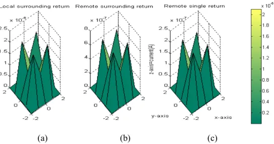
The single solar cell array stimulation chip with local surrounding return electrode has been designed and verified after the in vitro experiment. The silicon retina with solar cell array can successfully trigger the ganglion cells with threshold charge lower than 2.8nC with 75μm x 75μm stimulating electrode. Probed retinal stimulation current of solar cell array with local surrounding return electrode is 1.08μA, which is 10 times of remote surrounding return and 3 times of remote single return. Probed retinal stimulation current of two cascode solar cell array is 2.09μA, which is 2 times more current efficient than single solar cell array. Retina interface impedance has been measured by the multi-size microelectrode chip. Retina interface impedance decreases with increasing frequency, increasing electrode size and decreasing center-to-center distance of electrodes. At low frequency, retina interface impedance is over 1MΩ which is difficult for stimulation current generated from solar cell array to flow into retina. High potential of two cascode structure is one of the solutions to this problem. With local surrounding return electrode, optimum photo-sensing regions of each pixel of single and two cascode solar cell array stimulation chips are 14400μm2 and 19200μm2 and current stimulation efficiency with the optimum photo-sensing region of the latter is 1.65 times larger than the former.
In the work of four-block divisional power-supply stimulation chip, the capability of on-chip solar cell supply system integrated with circuit system in CMOS technology has been
proved, and the feasibility of using power supply system in turn to elevate power management efficiency has also been verified. Power control unit with original 1066 solar cells and extra 2540 solar cells is able to generate four power control signals, which are nonoverlapping and on different phases, to control each block of pixel array. Clock frequency is 1.5kHz under 15.8mW/cm2 incident light intensity with only 24.8nW power consumption. The output stimulating current of each pixel is approximately 1.1μA under same light intensity. Comparing with 16-pixel conventional solar cell array, which can only generate 0.31μ A at 15.8mW/cm2 for total 5003 solar cells, output stimulation current of four-block divisional power supply stimulation chip is 3 times higher and power efficiency is 4 times higher. The proposed power management structure could be considered as one of the highly integrated solutions for the efficient current stimulation CMOS chips of subretinal prosthesis.
Multi-size microelectrode chip and single solar cell array stimulation chip are fabricated with standard 0.35μm and tsmc process; two cascode solar cell array stimulation chip and four-block divisional power-supply stimulation chip are fabricated with standard 0.18μm tsmc CMOS process. The proposed efficient current stimulation chips all have contribution to the subretinal prosthesis.
ACKNOWLEDGEMENTS
致謝
首先誠摯的感謝指導教授吳重雨博士,讓我成為奈米晶片與系統實驗室(307實驗室) 的一份子。在吳教授循序漸進的教誨、無與倫比的耐心與滿懷愛心的鼓勵下,使我得以 獲得許多積體電路設計的專業知識,並不斷從問題中尋找到答案,更學會遭遇難題的解 決態度與方法。另外也要特別感謝和藹可親的師母曾昭玲女士,謝謝她不時給予我關懷 與鼓舞,讓我重新找回研究的熱忱。 此外,我還要感謝林伯剛醫師在醫學領域,與焦傳金老師在細胞電生理領域的指導 與協助,並感謝焦老師的學生楊雅婷學姊在量測過程中的協助,讓這份跨領域的研究能 夠順利完成。 在這段求學過程中,307實驗室給予了我完善的硬體及軟體資源,讓我能夠順利的 完成學業,全靠歷代學長姐們努力經營實驗室,讓實驗室如此成長卓越,並有相較於其 他實驗室更有系統的體制。另一方面也要感謝林俐如、陳勝豪、楊文嘉、陳煒明、王文 傑、黃祖德、蘇烜毅、蔡夙勇、劉麗珍、萬諶、許筱妊、蔡宗昀、陳偉丞、周敬程等實 驗室學長姐的細心指導,讓我的研究可以順利進行;另外也感謝及助理卓慧貞小姐與李 清音小姐,給予我在研究上的資源及行政上的幫助,讓我完成學業。 接著要感謝的是一起打拼的同學們:明翰、子薰、健軒、書瑾、旻毅、文杰、偉霖、 堂龍、詩翰、佑達等。大家一起努力修課、做考古題,熬夜趕工,出遊玩樂,讓我的碩 士生活增添風采。謝謝你們一直以來的陪伴與關懷,並互相扶持,加油打氣讓我能充電 再繼續努力。 最後,我要致上最深的感謝給予我最親近的父母親,由於他們一直以來的關心、支 持與無微不至的照顧,並用心的栽培我讀書,進而讓我擁有今日的成就。還要感謝姐姐 的幫助與鼓勵,及男友的照顧與陪伴,讓我在安逸與溫馨中念完碩士。最後祝福我的師 長、家人、朋友及學弟妹們事事順心、身體健康。我在撰寫的過程中,雖力求嚴謹,然 誤謬之處,在所難免,尚祈各位讀者賜予寶貴意見,使本論文能更加完善。 柳 慧 君 謹誌於竹塹交大 庚寅
夏CONTENTS
ABSTRACT (CHINESE)...
iABSTRACT (ENGLISH)...
iiiACKNOWLEDGEMENTS ...
vCONTENTS...
viTABLE CAPTIONS ...
viiiFIGURE CAPTIONS...
ixCHAPTER 1 INTRODUCTION ...
11.1 Background ... 1
1.2 Review on Epiretinal and Subretinal Prostheses ... 3
1.2.1 Epiretinal Prosthesis ... 3
1.2.2 Subretinal Prosthesis... 7
1.3 Motivation ... 11
1.4 Main Results and Thesis Organization... 12
CHAPTER 2 ANALYSIS OF RETINA INTERFACE
IMPEDANCE...
142.1 Electrode-Electrolyte Interface Properties ... 14
2.2 Chip Structure and Measurement Setup... 15
2.2.1 Chip Structure... 15
2.2.2 Retina Preparation and Measurement Environment ... 18
2.3 Measurement Results and Discussion ... 21
CHAPTER 3 SOLAR CELL ARRAY FOR EFFIENT
SUBRETINAL STIMULATION ...
263.1 Chip Structure ... 26
3.1.1 Solar Cell and Photodiode Structure... 26
3.1.2 Single and Two Cascode Solar Cell Array Stimulation Chips ... 28
3.2 Simulation Results ... 33
3.4 In Vitro Experimental Results... 43
3.5 Conclusions... 48
CHAPTER 4 FOUR-BLOCK DIVISIONAL POWER-SUPPLY
STIMULATION CHIP...
504.1 Chip Structure ... 50
4.2 Simulation Results and Layout Description ... 57
4.2.1 Simulation Results ... 57
4.2.2 Layout Description ... 60
4.3 Measurement Results ... 64
4.4 Discussion... 69
CHAPTER 5 CONCLUSIONS AND FUTURE WORK...
735.1 Conclusions... 73
5.2 Future Work ... 74
REFERENCES
...
76TABLE CAPTIONS
CHAPTER
2
Table I Electrode distances of row A and row E ... 16
Table II Summary of the microelectrode chip ... 17
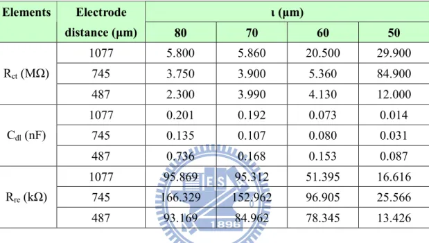
Table III Fitting results of retina interface impedance of big electrode sets... 23
Table IV Comparison of Humayun et al. in 2007 [22] and this work ... 25
CHAPTER
3
Table V Summary of the SSCA stimulation chip ... 29Table VI Summary of the TSCA stimulation chip... 30
Table VII Comparison of several subretinal studies with this work... 49
CHAPTER
4
Table VIII Sizes of the MOSFETs of each circuit ... 53Table IX Specification of the FBDP stimulation chip ... 54
Table X Comparison between the simulation and measurement results with the specification of the FBDP stimulation chip... 65
FIGURE CAPTIONS
CHAPTER
1
Figure 1.1 Cross-section of retina and implementation system of artificial retina prostheses. (Image courtesy of Webvision, webvision.med.utah.edu.)... 2 Figure 1.2 System overview of an epiretinal implant. (Reprinted from
http://www.cbse.ucsc.edu.) ... 6 Figure 1.3 Schematic of the retina implant with a retina encoder outside the eye and an implanted retina stimulator adjacent to the ganglion cell layer. (Reprinted from “Dialog concepts for learning retina encoders,” by R. Eckmiller)... 6 Figure 1.4 Schematic diagram of the wireless operation of the visual prosthesis system.
(Reprinted from “Development and implantation of a minimally invasive wireless subretinal neurostimulator,” by Rizzo and Wyatt)... 10 Figure 1.5 System overview of an subretinal implant. (Reprinted from “Optoelectronic retinal
prosthesis: system design and performance” by Jim Loudin et al., Stanford University) ... 11
CHAPTER 2
Figure 2.1 Equivalent circuit model of retina interface ... 15 Figure 2.2 (a) Electrode array patterm and (b) array description of the microelectrode chip.
Each column is composed of a small electrode set or both big and small electrode set. Totally 8 rows and 15 columns of multi-size microelectrodes are in this chip 18 Figure 2.3 Layout view of the microelectrode chip... 2 Figure 2.4 Chip micrograph of microelectrode chip. Whole chip size is 2.25mm x 1.30mm.
Metal connection between the stimulators and recorders is 1.5mm long... 20 Figure 2.5 (a) Shematic of measurement setup for measuring retina interface impedance. (b)
Photograph of impedance recording. Two wires of the wire-bounded microelectrode chip were connected to the probe of impedance analyzer ... 20 Figure 2.6 Frequency to impedance curve of (a) big electrode sets (b) small electrode sets. The space between 80-μm side length electrodes is 348μm; the space between 30-μm side length electrodes is 387μm ... 24 Figure 2.7 Distance to impedance curve of 60-μm side length electrodes. Measuring frequency is at (a) 40Hz, 0.5kHz, 1kHz and 1.5kHz (b) 25kHz, 50kHz, 75kHz and 100kHz ... 24 Figure 2.8 (a) Distance to impedance (Rct) curve of big electrode sets (b) distance to
capacitance (Cdl) curve of big electrode sets... 25
Figure 2.9 (a) Distance to resistance (Rs) curve of big electrode sets (b) distance to resistance
CHAPTER
3
Figure 3.1 Cross-sections of P+/N-Well solar cells with floating P-Substrate in 0.35μm 2P4M technology. The functions are driving passive loads with (a) photocurrent and (b) photovoltage... 27 Figure 3.2 Cross-section of P+/N-Well solar cell and NMOS in parallel connection in 0.35μm 2P4M technology. Leakage current is induced by parasitic BJT from nonfloating P-Substrate ... 27 Figure 3.3 Cross-sections of two N+/P-Well solar cells in series connection with floating P-Substrate in 0.18μm 1P6M technology. The functions are driving passive loads with (a) photocurrent and (b) photovoltage ... 28 Figure 3.4 Layout view of two SSCs in parallel connection... 30 Figure 3.5 Layout view of SSCA stimulation chip. Whole chip size is 0.976mm x 0.962mm
... 31 Figure 3.6 Layout view of two TSCs in parallel connection. Solar cells are built in the DNW ... 32 Figure 3.7 Layout view of the TSCA stimulation chip. Whole chip size is 0.976mm x 0.962mm ... 32 Figure 3.8 Schematic of a SCA implanted beneath the PRL ... 35 Figure 3.9 Schematic of the 3D spreading resistive network model. Thick, column and row
resistances are represented by Rt, Rc, and Rr, respectively... 36
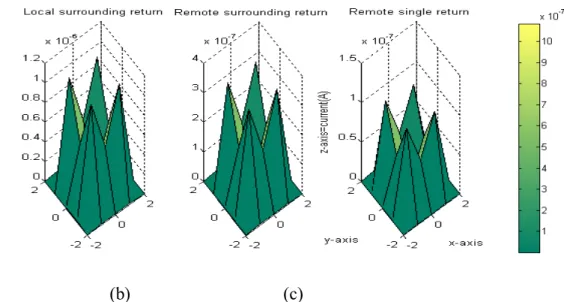
Figure 3.10 Schematic of the first layer of the retinal tissue. The retinal tissue we assumed is composed of 256 x 256 sets of resistances. The middle point of the matrix is at (0, 0). Stimulation site is labeled by the smallest square, 9 sets of resistances are included in a stimulating electrode. Probe region is labeled by the bigger square, 25 sets of resistances are included in the probe region ... 36 Figure 3.11 Three different kinds of return electrodes: (a) local surrounding return electrode, (b) remote surrounding return electrode and (c) remote single return electrode ... 37 Figure 3.12 (a) Illumination model and (b) simulation model of P+/N-Well solar cells. P+
with LV is connected to ground and N-Well with HI is connected to retina tissue . 37 Figure 3.13 Simulation results of stimulation current of three different return electrode
designs in SSCA: (a) local surrounding return, (b) remote surrounding return, and (c) remote single return... 37 Figure 3.14 (a) Illumination model and (b) simulation model of two cascode N+/P-Well solar cells. N+ with LV is connected to ground and P-Well with HV is connected to retina tissue ... 37 Figure 3.15 Simulation results of stimulation current of three different return electrode
designs in TSCA: (a) local surrounding return, (b) remote surrounding return, and (c) remote single return... 38
Figure 3.16 SSCA simulation results of stimulation current to different return electrode design curves of three different retina layers ... 38 Figure 3.17 (a) Electrode distance to current curves of SSCA and TSCA. Maximum current
occurs at electrode distances 32 and 64, respectively ... 38 Figure 3.18 (a) Solar cell numbers and (b) Photo-sensing region to current curves of SSCA
and TSCA. Maximum current (36.8nA and 60.6nA) occurs at solar cell numbers of 576 and 192 and photo-sensing regions of 14400μm2 and 19200μm2 for SSCA and TSCA, respectively... 39 Figure 3.19 Chip micrographs of one pixel of (a) SSCA and (b) TSCA stimulation chips .... 40 Figure 3.20 Measurement environment of the output current of SCA. The left part is a
microscope with 532nm laser light source. The chip in the middle part is placed on the Stage of the microscope. The left part is an auto-ranging Picoammeter ... 41 Figure 3.21 Measurement results of the (a) output current and (b) charge density of SSCA under various power of laser light source ... 42 Figure 3.22 Measurement results of the (a) output current and (b) charge density of TSCA
under various power of laser light source ... 42 Figure 3.23 Measurement environment of the IV curve. The left part is He-Ne laser light sources; the middle part is the chip setup middle, and the right part is the HP4145B parameter meter ... 42 Figure 3.24 Measurement results of the I-V curves of SSCA and TSCA stimulation chips
under He-Ne laser light source... 43 Figure 3.25 Schematic and a photograph of the measurement environment. Light source is
532nm laser, amplifying ratio of microscope is 40, the stimulating chip is placed beneath the PRL of isolated retina, and recording the signal from a loose patch on the ganglion cell layer (GCL) ... 45 Figure 3.26 Photographs of (a) ON alpha RGC; (b) OFF alpha RGC. White bar represent 100um and the size of this ganglion cell is about 1.2mm. These pictures are reprinted from NTHU Y.T. Yang ... 45 Figure 3.27 Responses of RGC before and after the light bleaching protocol... 46 Figure 3.28 (a) Cell soma locations on the SSCA stimulation chip and (b) relationship
between the threshold of RGCs upon electrical stimulation and their locations ... 46 Figure 3.29 Recorded signals of (a) ON alpha RGC and (b) OFF alpha RGC for 10 trails, 1000ms. Light source is 1-mW laser and stimulus duration is 10ms... 46 Figure 3.30 Relationship between electrical stimulation strength and RGC responses of (a) percent of responded trails, (b) first spike latency and (c) spike number... 47
CHAPTER
4
Figure 4.1 Schematic of 16-pixel (a) conventional SCA, (b) four-block divisional SCA and (c) eight-block divisional SCA... 54
Figure 4.2 Block diagram of the FBDP stimulation chip. Upper block: power control unit
(PCU); lower block: 16-pixel array... 55
Figure 4.3 Schematic of the pulse generator ... 55
Figure 4.4 (a) Block dagram and (b) schematic of the frequency divider ... 55
Figure 4.5 Schematic of the NAND gates and INV gates... 56
Figure 4.6 Schematic of the combinational logic circuits... 56
Figure 4.7 Schematic of the tapered buffer ... 56
Figure 4.8 Schematic of one pixel circuit. Output current (IOUT) is controlled by the NMOS switch with the control signal from PCU ... 57
Figure 4.9 Schematic of (a) current to voltage output convertor (b) two stage amplifier ... 57
Figure 4.10 Post-simulation results of (a) the clock generator and (b) buffered signals of the clock generator and frequency dividers under 3.60mW/cm2 light intensity... 58
Figure 4.11 Post-simulation results of the four buffered control signals under 3.60mW/cm2 light intensity... 59
Figure 4.12 Post-simulation results of the output stimulation current of each block under 3.60mW/cm2 light intensity ... 59
Figure 4.13 Monte-carol simulation results with 5% variation of the output stimulation current of each block under 3.60mW/cm2 light intensity ... 60
Figure 4.14 Post-simulation results of the output voltage of current to voltage convertors under 3.60mW/cm2 light intensity... 60
Figure 4.15 Post-simulation results of the voltage drop of 50kΩ resistances of the output electrodes under 3.60mW/cm2 light intensity ... 60
Figure 4.16 Cross-sections of a solar cell and (a) a NMOS and (b) a PMOS in parallel connection ... 62
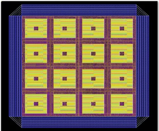
Figure 4.17 Layout of the four-block divisional power supply chip with control circuit and other test-key. The layout dimension is 1.350mm x 1.315mm ... 62
Figure 4.18 Layout of the PCU ... 63
Figure 4.19 Layout of a single pixel in the 16-pixel array... 63
Figure 4.20 Layout of the current monitor amplifier and Rout ... 63
Figure 4.21 Chip micrograph of the FBDP stimulation chip ... 66
Figure 4.22 Measurement environment of the PCU test-key. Left part: high brightness LED flashlight with a convex lens; middle part: chip setup; right part: 4-recording channel oscilloscope ... 66
Figure 4.23 Measurement results of the clock generator and frequency dividers under 92.3mW/cm2 light intensity ... 67
Figure 4.24 Measurement results of the control signals under 92.3mW/cm2 light intensity... 67
Figure 4.25 Measurement environment of the PCU test-key. Left part: middle brightness LED flashlights; middle part: chip setup wth an external solar cell power supply; right part: 4-recording channel oscilloscope ... 67
Figure 4.26 Measurement result of the voltage supply of PCU under 15.8mW/cm2 light intensity with extra 2540 external or 5003 internal solar cells. Voltage level increases to 0.5V... 68 Figure 4.27 Measurement results of the clock generator and frequency dividers under 15.8mW/cm2 light intensity with extra 2540 external or 5003 internal solar cells. Voltage level is 0.5V as the VDD of tapered buffer ... 68 Figure 4.28 Measurement results of four different phase control signals under 15.8mW/cm2 light intensity with extra 2540 external or 5003 internal solar cells. Voltage level is 0.5V as the VDD of tapered buffer... 68 Figure 4.29 Measurement environment of the pixel array. Left part: middle brightness LED flashlights; middle part: chip setup wth an external solar cell power supply; right part: 4-recording channel oscilloscope ... 69 Figure 4.30 Measurement results of four different phase signals of output current from the voltage drop of external 50kΩ resistances. With 2540 extra external solar cells for PCU, voltage level is 55mV under 15.8mW/cm2 light intensity. ... 69 Figure 4.31 Measurement and simulation I-V curves of the solar cell test-key under
73.2mW/cm2 light intensity of laser ... 71 Figure 4.32 Measurement and simulation loading to positive voltage curves of the solar cell
test-key under 73.2mW/cm2 light intensity of laser ... 71 Figure 4.33 Equivalent circuit model of a solar cell. Iph represents the photocurrent, Rsh is the
shunt impedance and Rse is the series impedance. Currents pass through solar cell,
Rsh and Rse are Id, Ish and Io, respectively... 72
Figure 4.34 Pre-simulation results of the buffered signals of clock generator and frequency dividers with new solar cell model. Power supplies of the PCU are (a) 1066 solar cells and (b) 3606 solar cells. VDD of the tapered buffer is 0.7V ... 72
CHAPTER 1 Introduction
1.1
Background
Vision is one of the most important sensory organs and thus losing vision can bring one endless torments. The vertebrate retina can perform two functions. Firstly, the photoreceptors (rods and cones) are able to transducer the information of the optical image into neural signals. Secondly, the neural circuitry is able to abstract certain features of the visual world. Via optic nerve fibers, the features can form large number of photoreceptor signals and pass the information on to the brain.
Currently, over 10 million people worldwide are afflicted with photoreceptor degenerative diseases that reduce vision to bare light perception or complete blindness [1]. Retinitis pigmentosa (RP) is the leading cause of inherited blindness with 1.5 million people worldwide affected and an incidence of 1/3500 live births. Also, age-related macular degeneration (AMD) is the leading cause of visual loss among adults older than 65, with 0.7 million patients newly diagnosed annually in the United States, 1/10 of whom become legally blind each year [2]. Once photoreceptors are nearly completely lost, such as in end-stage RP or AMD, very few approaches can restore useful vision to blind patients. One possible avenue that has been explored is to use implantable microelectronics. The different methods currently being pursued to electrically stimulate damaged areas of the visual system include electrical and neurotransmitter stimulation of the retina, as well as the use of light-sensitive nano-particles. Implantable methods can be categorized by the extraocular or intraocular sites of device implantation.
Extraocular implantation includes the visual cortex and optic nerves. Dobelle’s 64-channel platinum electrode surface stimulation prosthesis of the occipital cortex was shown to allow blind patients to recognize 6-inch characters at 5 feet [3]. However, this prosthesis encountered several difficulties including controlling the number of phosphenes induced by each electrode. The optic nerve is a dense neural structure with approximately 1.2 million axons confined within a 2-mm diameter cylinder [4]. While this allows the entire visual field to be represented in a relatively small area, it remains difficulties to achieve focal stimulation of neurons and to decipher the exact retinotopic distribution of the optic nerve.
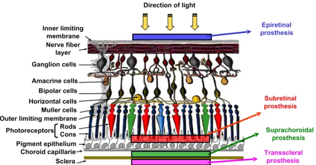
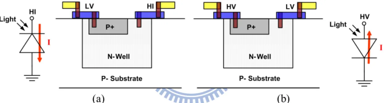
intraocular implantation sites. Four prostheses are well known; these include the transscleral, suprachoroidal, subretinal and epiretinal prostheses. Four different implantation sites are shown in Fig. 1.1, transscleral prostheses are implanted on the sclera; suprachoroidal prostheses are implanted on the choroid; subretinal prostheses are implanted between the pigment epithelial layer and the degenerated photoreceptors; epiretinal prostheses are implanted onto the inner retinal membrane.
Transscleral and suprachoroidal stimuli were designed to minimize insult to the retina by electrode stimulation. The fibers of the electrode of the transscleral implantation were placed on the lower bulbar conjunctiva 5mm from the corneal limbus [5]. The anodic stimulating electrode of the suprachoroidal implantation was positioned on the choroidal membrane and the cathode was placed in the vitreous body [6]. Due to less direct stimulation of the retina, the threshold charge densities of these two prostheses were as large as 318μC/cm2 [5] and 790μC/cm2 [7], respectively, which are higher than direct stimulation of the retina. Subretinal prostheses are trying to directly stimulate the remaining intact retinal neurons—bipolar or horizontal cells, the initial neuronal processing stage of the retina—by currents generated from photodiodes or electrodes. Epiretinal implants have been designed to directly stimulate retinal ganglion cells—the final and intricate retinal processing stage—with an electrode array.
The majority of the groups currently working in visual prosthetics are concentrating either on epiretinal (e.g., [8-14]) or subretinal (e.g., [15-21]) electrical stimulation. In the next section, we will review on these two prostheses.
Figure 1.1 Cross-section of retina and implementation system of artificial retina prostheses. (Image courtesy of Webvision, webvision.med.utah.edu.)
1.2
Review on Epiretinal and Subretinal Prostheses
1.2.1
Epiretinal Prosthesis
The idea of the epiretinal prosthesis resembles that idea of the cochlear implant. The cochlear implant converts sound into electrical impulses to stimulate the auditory nerve in the inner ear. The conceptual prosthetic system of Fig. 1.2 shows that the epiretinal prosthesis involves the capture and digitization of images from the external world with a device such as a camera. These images are transformed into patterns of electrical stimulation, which are used to excite remaining, viable inner retinal neurons. Significant power and data telemetry mechanisms are required to drive this process. Several groups worldwide have developed different designs of epiretinal implants that vary in terms of the intraocular and external elements which constitute the devices and how they function to enable vision in patients. They were all guided by similar requirements, which included preserving as much of the normal anatomy/physiology of the eye as possible while minimizing the amount of implanted electronics required to power the device [8]. Three such approaches are described below.
The Intraocular Epiretinal Prosthesis (IRP) was initiated by a team led by Dr. Mark S. Humayun at the Doheny Eye Institute of the University of Southern California. IRP was composed of a pair of glasses housing a miniature video camera, an external visual processing unit, an intraocularly implanted stimulating electrode array, and inductive coil for wirelessly relaying power and data. The visual processing unit acquired and digitized video input from the camera, applied various filters on the image (e.g. edge detection, contrast enhancement, difference of Gaussian), and downscaled the resolution to a 6 x 10 grid. This processed information, in the form of controlled patterns of electrical pulses, was then transmitted into the eye by magnetic coils of the inductive link telemetry system and sent to the temporal skull. The microelectrodes on the array applied these pulses to stimulate any viable inner retinal neurons. The array was positioned just temporal to the fovea and was attached to the inner retinal surface using a single tack, which was inserted through the electrode array into the sclera as shown in Fig. 1.2 [9].This 60-pixel image was then mapped to a stimulation intensity using customized look-up tables that have been derived from testing of individual patients. To date, 21 patients with degenerated photoreceptors have received the 60-electrode device. Seventeen patients described visual
perceptions of retinotopically consistent phosphenes that were seen when local current was applied to the surface of the retina with the implanted electrodes. At the 6th month followed up testing points, average success rates of touching the door with the system on and off were 59% and 32%; tracking the line until the end with the system on and off were 44% and 26%. With a perceptual threshold ranging from 24μA to 702μA (1 ms pulse), patients were not only able to distinguish the direction of motion of objects but also to discriminate between percepts created by different electrodes based on their locations. These phenomenons demonstrate that retinotopic organization is not lost when a patient loses sight [10].
The Learning Retina Implant (LRI) was developed by a consortium of 14 expert groups in Germany directed by Rolf Eckmiller since 1995. LRI also comprised of intraocular and extraocular components. The retina encoder (RE), which approximated the typical receptive field properties of retinal ganglion cells, replaced the visual processing capabilities of the retina by means of 100 to 1000 individually tunable spatiotemporal filters. The RE was situated in the frame of a pair of glasses or embedded in a contact lens. The processing of visual information that occurd in the RE simulated the filtering operations performed by individual ganglion cells. The RE output was then encoded and transmitted via a wireless signal and energy transmission system to the implanted retina stimulator (RS). The RS was a ring-shaped, soft micro-contact foil centered about the fovea that was affixed to the epiretinal surface and must be in contact with a sufficient number of retinal ganglion cells/fibers to elicit electrical spikes as shown in Fig. 1.3 [11]. Visual patterns were mapped onto spike trains for the contacted ganglion cells through the REs. The REs not only simulated the complex mapping operation of parts of the neural retina, but also provided an iterative, perception-based dialogue between the RE and human subject. The purpose of this dialogue was to tune the various receptive field filter properties with information “expected” by the central visual system to generate optimal ganglion cell codes for epiretinal stimulation. In order to optimize the dialog between the retina encoder and the central visual system, proper stimulation coding of electrically induced neural signals for the retinal ganglion cells in contact with the RS needed to be determined [12]. Clinical trials primarily focusing on testing of the learning implant and dialogue-based RE tuning had being done but no much success has been reported so far.
A third epiretinal prosthesis was developed by Joseph 3rd Rizzo and John Wyatt at the Harvard Medical School. Their version of an implant was similar to that of the IRP group in that it consisted of distinct intraocular and extraocular modalities. The
intraocular components were composed of a photodiode panel and a stimulator chip that were affixed, away from the retinal surface, onto a modified intraocular lens. A flexible 10-μm thick polyimide electrode array was implanted onto the retina, rather than held above the retinal surface, as performed by Humayun et al., and attached to the epiretinal surface using a small gold weight and a viscoelastic made of hyaluronic acid. The extraocular unit was composed of a charge coupled device camera, a signal processing unit, as well as a laser, all mounted onto a pair of glasses. The battery back which powered the device was also located external to the eye. The photodiode panel captured the processed signal from a laser pulse emitted from the glasses and the stimulator chip then delivered this information to the microelectrode array on the epiretinal surface of the eye [13]. Implantation in 5 blind patients with RP and 1 normal-sighted patient who was scheduled for enucleation due to orbital cancer had been done. Similar to the results found by the IRP group, they observed that higher charge densities were required to stimulate the retinas in patients with worse vision, with the 400-μm electrode in blind patients charge density thresholds were 0.28 to 2.8mC/cm2. No apparent damage as a result of electrical stimulation of the retina was evident of the normal-sighted patient’s eye. The results from their short-term studies in 5 patients were mixed and inconclusive. Simple pattern vision was not achieved by either the blind or the normal sighted patients when multi-electrode patterns of electrode stimulation were applied in trials with multiple electrodes [14]. Due to the inability of getting good or consistent results with epiretinal stimulation, Rizzo and Wyatt have abandoned the epiretinal approach and are now developing a subretinal approach.
Some disadvantages come along with advantages in these prostheses. Firstly, with inductive coil for wirelessly relaying power and with electrical pulses from wiring, microelectrodes on the array can stimulate any viable inner retinal neurons for sufficient power supply. But, heat dissipation by intraocular prosthesis components may cause elevated temperature and thus damage the eyeball. Secondly, the implementation of the prosthesis onto the retina may carry on pixel-tuning after surgery easily, but this also means that fixation of electrode array requires some of retinal tack which can dislodge, e.g. due to trauma. Besides, in conjunction with the foreign material of the array as well as electrical impulses deliver to the implant could possibly result in fibrous encapsulation of the tack. Thirdly, in most cases, both intraocular and extraocular components are required to make good functions. Limited area of epiretinal space will greatly confine the goal of implantation of 1000-electrode epiretinal prosthesis. Lastly, in order for a desired visual percept to be generated by
the central visual system, significant information in the form of electrically induced neural signals must not only be provided by the retina stimulator or encoder system but also be clear or unambiguous for interpretation by the brain, therefore, stimulation sites uncertainty is a big challenge.
Figure 1.2 System overview of an epiretinal implant. (Reprinted from http://www.cbse.ucsc.edu.)
Figure 1.3 Schematic of the retina implant with a retina encoder outside the eye and an implanted retina stimulator adjacent to the ganglion cell layer. (Reprinted from “Dialog concepts for learning retina encoders,” by R. Eckmiller).
1.2.2
Subretinal Prosthesis
The fundamental concept of the subretinal approach is to restore vision by means of prosthesis involves the implantation of micro-photodiode array between the bipolar and horizontal cell layer and the retinal pigment epithelium. Subretinal implants are trying to stimulate the ganglion cell layer through the remaining intact retinal neurons by currents generated from photodiodes or electrodes. Implants act like photoreceptors and its stimulation on the ganglion cells may result in a correlated stimulus in location and a perceived stimulus in vision. Four such approaches are described below and are categorized by the power sources. Passive devices rely on incident light for power, whereas active devices have external power sources.
The first passive device was developed by Alan and Vincent Chow of Optobionics Corp, who believed that a subretinal implant could function as a simple solar cell without the need for a power or input source of any type [15]. Their Artificial Silicon Retina (ASR) Microchip was powered entirely by light entering the eye, without batteries or other ancillary devices. Two millimeters in diameter, the ASR contained approximately 3500 microelectrode-tipped micro-photodiodes which converted incident light into electrical signals similar to those normally produced by the retina’s own photoreceptors. The photodiodes had a photoelectric efficiency of 0.45A/W per cm2 and developed a maximum compliance voltage of 450 mV with a 1 MΩ resistance. These electrical impulses, in turn, stimulated any viable retinal neurons, which then processed and sent these signals to the visual processing centers in the brain via the optic nerve. As part of a safety and feasibility study, the ASR Microchip was implanted in 6 patients, with a follow-up of 6 to 18 months. Some of the patients had reported improved visual function away from the implant site, suggesting that the presence of the implant alone, or coupled with low-level electrical stimulation, induced a “neurotrophic effect” that improved the health of the retina and consequently improved visual function. However, the reports demonstrated that the idea behind this simple approach is not feasible, because it lacked a source of viable power and stimulating charge density was only 0.1nC/cm2 [16].
An active device for a subretinal implant was initiated by a consortium of research universities in Germany since 1996 under the guidance of Eberhart Zrenner. Their subretinal Integrated Circuit (IC) was composed of a micro-photodiode array which contained approximately 1500 microelectrodes in a checker-board pattern configuration and served to modulate current pulses based on the amount of light incident on the photodiode [17]. A micro-fabricated cable that passed out of the orbit
and crossed the skin behind the ear supplied command and configuration signals as well as power to the subretinal IC. Because such a cable arrangement is a potential infection source, the implant was limited to 30 days. This implant also included 16 “direct stimulation” electrodes, and the electrodes were not activated by the subretinal IC but were directly connected to the cable and were activated by external equipment. Due to packaging limitations, the subretinal IC did not function in all of the implants. Direct stimulation electrodes were able to elicit responses in all subjects [18]. This device applied constant voltage stimulation and adequate stimulus levels (1–2.5 V for 0.5-6ms) to generate perceptions. In recent reports, 11 patients received subretinal implants. Subretinal multi-electrode implants with charge close to recognition threshold (10 to 27nC/ electrode or 0.4mC/cm2 to 1.08mC/cm2) produced correct patterns that allowed for the recognition of individual letters even at low luminance levels [19]. This clearly supports the feasibility of light sensitive subretinal multi-electrode devices for restoration of useful visual percepts in blind patients.
Another type of active device subretinal prosthesis was recently developed by Rizzo and Wyatt. The size of the implanted device is 12mm x 31mm. Schematic diagram of the wireless operation of the visual prosthesis system is shown in Fig. 1.4. A camera and transmitter collected and then rebroadcasted an image signal to the implanted stimulator chip, which was to retransmit biphasic current pulses, in patterns corresponding to the desired image, to the stimulating electrode array located in the subretinal space. The implant positioned large coil and electronics structures at a distance of approximately 1.5cm from each other; thereby the device may be implanted in the superior nasal and superior temporal quadrants of the ocular orbit. The middle section of the device contained only the polyimide host flexible circuit and a large reference/return electrode, which could be implanted underneath the superior rectus muscle. Only the flexible, 16-μm thick polyimide array with iridium oxide (IrOx) stimulating electrodes enters the scleral flap, which was typically made 10mm posterior to the limbus. The chip, capable of delivering up to 775μA stimulation current, drove 15 electrodes with 15 current-source drivers. Though this project is still in its early stages of development, they have reported that biocompatibility studies examining the effects of a foreign material in the subretinal space as well as surgical methods to implant their device have been extensively evaluated. While their results have been encouraging to date, further studies regarding the long-term biocompatibility of materials in the subretinal space as well as methods to protect the retina upon insertion of the prosthesis during surgery will need to be performed before a clinical trial is conducted to determine the safety and efficacy of
their implant in blind patients [20].
A second type of passive device subretinal prosthesis was recently developed by Jim Loudin et al. of Stanford University. Unlike the project done by Alan and Vincent Chow, which no image processing system was involved, they developed a retinal prosthesis system shown schematically in Fig. 1.5. Video stream from a miniature camera was processed and imaged onto the retinal implant by a video goggle projection system using 905nm near-infrared light. This wavelength is practically invisible to photoreceptors, and therefore does not interfere with any residual vision. However, it could be detected by implanted photodiodes, which converted pulsed (~0.5ms) light into pulsed electric current, with charge injection maximized by specially optimized photodiode circuits. This system delivered information to all pixels in parallel and scaled large numbers of pixels straightforward. Also, image processing was adjustable and many separate arrays could be implanted to expand the field of view. Several circuit diagrams of the photoconductive and photovoltaic cells were developed. One, two, and three diodes in series connection were studied in both anodal and cathodal polarities. With 50-μm side length sputtered iridium oxide film (SIROF) square electrodes and illuminating 0.3-mW light power per diode, the charge injection per photo-sensing region and stimulating charge density of a cathodal or an anodal diode were only 0.29nA/μm2 and 0.2mC/cm2, respectively. Among the developed structures, an anodally biased photoconductive circuit generated the greatest charge injection (1.6nA/μm2 and 1.1mC/cm2). These values were million times of a single photodiode developed by Alan and Vincent Chow. Although this project is still in its early stages of development, prostheses of pixel densities from 16pix/mm2 to 256pix/mm2 have been designed, simulated, and prototyped. Retinal tissue response to subretinal implants made of various materials has been investigated in RCS rats [21]. The prosthesis is expected to provide sufficient charge injection for high resolution retinal stimulation without the requirement for implantation of any bulky discrete elements such as coils or wiring.
The approaches of subretinal prostheses, like other methods of artificial vision, have its distinct advantages and disadvantages. One advantage is that the micro-photodiodes of a subretinal prosthesis directly replace the functions of the damaged photoreceptor cells while the retina’s remaining intact neural network is still capable of processing electrical signals. Placement of the subretinal prosthesis in closer proximity to any remaining viable inner retinal neurons in the visual pathway may be advantageous in decreasing current requirement for stimulation. In addition to the relative ease in positioning and fixing the micro-photodiodes in the subretinal
space, the lack of mechanical fixation allows for less surgically induced trauma upon implantation. Unlike the epiretinal prostheses, external cameras or image processing units are not required and the patients’ eye movements can still be used to locate objects. With photodiodes as power supply rather than wire-line connections, no difficulties are in keeping sterile and scarring problems are less.
One of the disadvantages of active devices is the limited area of the subretinal space, which contains the microelectronics, predisposes the contacted retinal neurons to an increased likelihood of thermal injury resulting from heat dissipation of wiring. Additionally, if the subretinal implant is only composed of an electrode array with the electronics outside the eye, then the prostheses must have a cable piercing the sclera leading to potential tethering on the cable. The tethering effect on the electrode array in the subretinal space can lead to possible movement after implantation as well as the more invasive transchoroidal incision and extensive subretinal bleeding.
On the other hand, the main disadvantage of passive devices is that stimulation current of the device is in proportion to photo-sensing region of each pixel, and thus limited area of the subretinal space confines the stimulation efficiency or resolution of this prosthesis. Thereby to improve the current stimulation efficiency of passive devices in a limited area of subretina is the major concern of this prosthesis.
Figure 1.4 Schematic diagram of the wireless operation of the visual prosthesis system. (Reprinted from “Development and implantation of a minimally invasive wireless subretinal neurostimulator,” by Rizzo and Wyatt).
Figure 1.5 System overview of an subretinal implant. (Reprinted from
“Optoelectronic retinal prosthesis: system design and performance” by Jim Loudin et al., Stanford University).
1.3
Motivations
To develop efficient current stimulation CMOS chips with passive devices for subretinal prosthesis, three major concerns are listed below.
A dense current stimulation chip with a small electrode per pixel is desirable to achieve maximum visual acuity. However, the output load of a stimulator is retina interface impedance. The impedance would vary with the size of electrodes [22]. Smaller electrode size results in a larger output load. Besides, with different return electrode to stimulating electrode distances, retina interface impedance ought to be different. Photocurrent, generated from a passive device, could barely stimulate the retina if the output load is too large compared with photoresistance. Therefore, to measure retina interface impedance with multi-size microelectrodes and different return electrode to stimulating electrode distances is the first priority in the design of retinal prostheses.
Solar cell array stimulation chip with multi directions of return path could enhance the stimulation efficiency [23]. Thus the shape of return electrodes is also relative to the current stimulation efficiency. Different kinds of return electrode have to be designed and evaluated the best one. Solar cell array with thousands of solar cells and
the best return electrode type can stimulate retina cells with large photocurrent. Solar cell with many two cascode solar cells and the best return electrode type can stimulate retina cells with even large current because of large photovoltage. Resolution of the photodiode arrays larger than 16 pixels can mimic partial photoreceptors well [24].
Power management efficacy of solar cell array can be elevated by redistribution of solar power to pixel array. One method is to facilitate the refractory period of vision. The retinal stimulation chips need not to stimulate the retina cells continuously but discretely. The maximum frame rate which can be distinguished by human is about 60Hz, namely, stimulating retina cells every 16ms or less, the brain of a patient still consider discrete stimuli as continuous ones. Applying the power control unit to the pixel array, each pixel activates in accordance with divisional blocks and uses solar cell power supply in turn. Output stimulation current and power efficiency are proportional to the divisional block numbers.
1.4
Main results and Thesis Organization
Four chips had been made in the development of efficient current stimulation CMOS chips for subretinal prosthesis.
First chip is multi-size microelectrode chip which was fabricated with standard 0.35μm tsmc process. The function is to measure retina interface impedance. From the measurement and analysis results, retina interface impedance not only decreases with increasing frequency and increasing electrode size but also decreases with decreasing center-to-center distance of electrodes. The analyzed retina impedance is in the range of 10kΩ to 200kΩ with 50-μm to 80-μm side length square electrodes.
Second chip is single solar cell array stimulation chip and was also fabricated with standard 0.35μm tsmc process. The main function of this chip is to efficiently stimulate retina cells with large photocurrent by 2540 parallel solar cells in each pixel. The other one is to mimic photoreceptor cells with 16 pixels. With 3-dimensional spreading resistive network simulation model, stimulation current passing through thick retina resistance of single solar cell array with local surrounding return electrode is 1.08μA, which is 10 times of remote surrounding return and 3 times of remote single return. By using the local surrounding return, optimum photo-sensing region of solar cells is 14400μm2 and maximum photocurrent per photo-sensing region is 2.55pA/μm2. The stimulation chip with single solar cell array and 75μm x 75μm stimulating electrode can successfully trigger the ganglion cells with low threshold
charge of 2.8nC, which is 3.5 times lower than Zrenner et al. in 2009 [19].
Third chip is two cascode solar cell array stimulation chip which was fabricated with standard 0.18μm tsmc process. The main function is to efficiently stimulate retina cells with high photovoltage by connecting two solar cells in series. With 414 parallel two cascode solar cells, stimulation current passing through thick retina resistance is 2.09μA, which is 2 times more current efficient than single solar cell array. By using the local surrounding return, optimum photo-sensing region of solar cells is 19200μm2 and maximum photocurrent per photo-sensing region is 3.15pA/μm2.
Fourth chip is four-block divisional power-supply stimulation chip which was also fabricated with standard 0.18μm tsmc process. The purpose of this chip is to increase power management efficiency and current efficiency with divisional power control system. The time interval between neighboring activation of the same pixel is smaller than refractory period of the retina cell thus to provide continuous signals for the brain. Power control unit with original 1066 solar cells and extra 2540 solar cells is able to generate four power control signals, which are nonoverlapping and on different phases. Clock frequency is 1.5kHz under 15.8mW/cm2 incident light intensity with only 24.8nW power consumption. The output stimulation current is approximately 1.1μA under the same light intensity. Comparing with 16-pixel conventional solar cell array, which can only generate 0.31μA at 15.8mW/cm2 for total 5003 solar cells, output stimulation current per pixel of four-block divisional power supply stimulation chip is 3 times higher. The capability of on-chip solar cell supply system integrated with circuit system in CMOS technology has been proved, and the feasibility of using the power supply system in turn has also been verified.
The remainder chapter of this thesis is organized as follows:
Chapter 2 describes the method to stimulate isolated retina and to record retina
interface impedance from stimulators and recorders of multi-size microelectrodes, also analyzes three components of interface impedance by model.
Chapter 3 compares electrical characteristic and current stimulation efficiency of
single and two cascode solar cell array, simulates three different designs of return electrodes, and records electrical responses of isolated rabbit’s retina.
Chapter 4 considers the divisional architecture of current stimulation chips that
integrate solar cells and CMOS technology together. The chips were designed, measured, and verified as a power efficient method of subretinal prosthesis.
Chapter 5 concludes our research presented in this thesis and puts forth some
CHAPTER 2 Analysis of Retina Interface
Impedance
2.1
Electrode-Electrolyte Interface Properties
Impedance of the retina interface largely defines the output load of a stimulator. To guide the design of a retinal prosthesis, understanding the electrical interface properties of retina is important. Retina interface is composed of electrode-electrolyte interface and electrolyte-retina interface. Retina interface impedance can be represented by an equivalent circuit model as shown in Fig. 2.1. The model of electrode-electrolyte interface comprises an interface capacitance (Cdl), which is
shunted by a charge transfer resistance (Rct) and in series with a solution resistance
(Rs) [22]. The model of electrolyte-retina interface consists of Rs and retina
impedance (Rre) in series connection.
The nonfaradaic impedance arising from the Cdl is constant phase angle
impedance (ZCAP), which is given by the empirical relation:
0 1 ( ) ( ) ( ) n CAP n dl Z Y j j C
where Y0 equals Cdl -n, n is a constant representing inhomogeneities in the surface and
ω is angular frequency. In a Nyquist plot the angle between the data and the abscissa axes n gives according to n=2θ/π, and n=1 represents a purely capacitive impedance element corresponding to the interface capacitance. Taken to be the series combination of the double layer capacitance and the diffuse layer capacitance, Cdl is
in proportion to the electrode size. Rct is a faradaic resistance given by the
experimental relation: 1 ct R J q and
J
J F
0RT
where is J the measured current density, q is the charge on the ion in the electrolyte. F is Faraday’s constant, η is the applied over potential, R is the gas constant, and T is the temperature. J0 is the equilibrium exchange current density which is composed of
reduction reaction rate constant and concentration of electron-acceptor ions, etc. The resistance measured between the working electrode and the reference electrode is termed to be Rs. Under the assumption that the counter electrode is infinitely large and
the working electrode is surrounded by electrolyte, Rs can be determined from the
spreading resistance which is encountered by current spreading out into solution. For a square electrode and a round electrode, the spreading resistances are given by
ln 4
s squareR
l
and4
s roundR
r
where ρ is the solution resistivity, 72 Ωcm for physiological saline, ι is the electrode side length of a square electrode and r is the radius of a round electrode.
Looking into the theoretical equations, three components of electrode-electrolyte interface impedance are all relative to electrode size. Therefore, the approximate value of retina impedance can be obtained from measurement of retinal interface impedance with muti-size microelectrodes.
Figure 2.1 Equivalent circuit model of retina interface.
2.2
Chip Structure and Measurement Setup
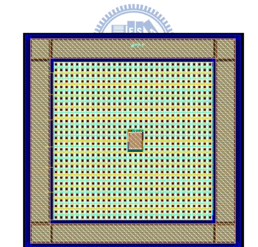
2.2.1 Epiretinal Prosthesis
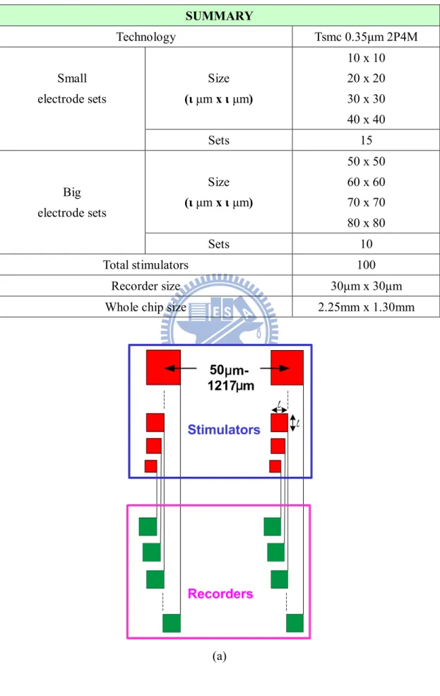
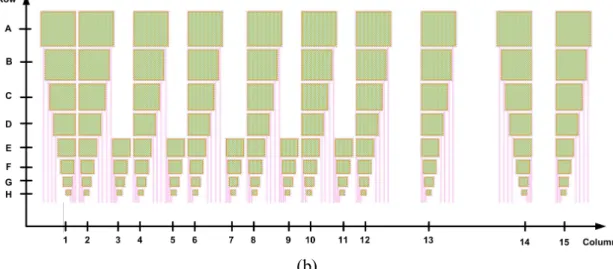
The electrode array pattern we designed is shown in Fig. 2.2(a). One stimulator was connected to one recorder. Electrode side length of a square stimulator, ι, is ranging from 10μm to 80μm. Electrode side length of a square recorder is 30μm which is the minimally bond-wired size of the COB apartment of IST, Inc. Separating eight kinds of ι into two groups, 10μm, 20μm, 30μm and 40μm are “small electrode set” and 50μm, 60μm, 70μm and 80μm are “big electrode set.” Center-to-center return electrode to stimulating electrode distance is called “electrode distance.” To confirm the relationship between different electrode distances and retina impedances, the distance between each column is ranging from 50μm to 1217μm. The detailed
description of the electrode distances between column 1 and other columns of electrodes is in Table I. Column 1 to column 15 and row A to row H are labeled in Fig. 2.2(b). Columns from left to right are defined as column 1, column 2…, to column 15; the rows from top to bottom are defined as row A, row B…, to row H. Electrode sizes of row A and row E are depicted here; ι of row A is 80μm and ι of row E is 40μm. The electrode distances of rows B, C, D are the values of the row A minus 10μm, 20μm and 30μm, respectively; the spaces of rows F G, H are the values of the row E minus 10μm, 20μm and 30μm, respectively. Whole chip layout view of multi-size microelectrode chip (microelectrode chip) is shown in Fig. 2.3, 10 columns were composed of both small and big electrode sets and 5 columns contained small electrode sets only, totally 15 columns. To sum up, 100 stimulators and relatively 100 recorders were designed as a planar microelectrode chip. The middle part of Fig. 2.3 is 1.5-mm long metal routing, connecting stimulators and recorders together. The long routing length ensures a minimum glue overflow effect. Summary of the microelectrode chip is shown in Table II. Whole chip size is 2.25mm x 1.30mm.
Table I Electrode distances of row A and row E
Row A Row E Column Electrode distances (μm) Column Electrode distances (μm) 2 90 2 50 - - 3 129 4 219 4 179 - - 5 258 6 348 6 308 - - 7 387 8 487 8 447 - - 9 526 10 616 10 576 - - 11 655 12 745 12 705 13 898 13 859 14 1077 14 1077 15 1217 15 1177
Table II Summary of the microelectrode chip SUMMARY Technology Tsmc 0.35μm 2P4M Size (ι μm x ι μm) 10 x 10 20 x 20 30 x 30 40 x 40 Small electrode sets Sets 15 Size (ι μm x ι μm) 50 x 50 60 x 60 70 x 70 80 x 80 Big electrode sets Sets 10 Total stimulators 100 Recorder size 30μm x 30μm Whole chip size 2.25mm x 1.30mm
(b)
Figure 2.2 (a) Electrode array patterm and (b) array description of the microelectrode chip. Totally 8 rows and 15 columns of multi-size microelectrodes are in this chip.
Figure 2.3 Layout view of the microelectrode chip.
2.2.2 Retina Preparation and Measurement Environment
Chip micrograph of the microelectrode chip is shown in Fig. 2.4. Whole chip size is 2.25mm x 1.30mm and metal connection between the stimulators and recorders is 1.5mm long. The space between neighboring recorders in the same column is only 1μm, which is impossible to wire-bond all 100 recorders on a PCB. Thereby we
separated the fabricated chips into two wire-bonded types because of the dense layout structure. “Big electrode chip” contains big electrode sets only, that is, columns 1, 2, 4, 6, 8, 10, 12, 13, 14, and 15 are involved. “Small electrode chip” contains small electrode sets only. The small electrode sets are even denser than the big electrode sets, so we bonded columns 1, 2, 7, 12, 13, 14, 15 in this version only. In case that electrical responses of the recorders would also stimulate the retina and result in disturbance of the measurement. Recorders of the microelectrode chips have to be sealed with black glue after bonding.
The isolated retina we used was retina tissues from adult New Zealand White rabbits (1-2 kg). The animal was anesthetized with an intramuscular injection of 1:1 mixture of ketamine (50mg/ml) and xylazine (20mg/ml). A local anesthetic (proparacaine hydrocholoride; 2-3 drops) was been applied to the eye before intraocular injection of 4’, 6-diamidino-2-phenylindole (DAPI, 2μg; Sigma, St. Louis, MO). The animal was allowed to recover. The deeply anesthetized animal will be euthanized with overdose of anesthetic or 100% CO2. One day after DAPI injection,
the animal was dark-adapted for at least one hour before dissection. The animal was deeply anesthetized again for isolating the retina. Hemi-sectioned in oxygenated (95% O2 and 5% CO2) Ames’ medium, each eye was removed and the retina was dissected
out from the sclera and carefully peeled off the pigment epithelium.
At the beginning of the experiment, we put a self-made recording chamber on the wire-bonded microelectrode chip and poured in some balanced salt solution (BSS) to ensure biocompatibility of the retina. Then the prepared retina was cut into a small piece (diameter<5mm) and moved into the chamber. We pressed down the retina to the microelectrode chip by weights of a filter paper as shown in Fig. 2.5(a). To measure interface retina impedance, we used an impedance analyzer (4294A, Aglient, Inc) as shown in Fig. 2.5(b) to probe the impedance between a stimulating electrode and a return electrode. Two wires of the wire-bounded microelectrode chip were connected to the probe of impedance analyzer.
Figure 2.4 Chip micrograph of microelectrode chip. Whole chip size is 2.25mm x 1.30mm. Metal connection between the stimulators and recorders is 1.5mm long.
(a)
(b)
Figure 2.5 (a) Shematic of measurement setup for measuring retina interface impedance. (b) Photograph of impedance recording. Two wires of the wire-bounded microelectrode chip were connected to the probe of impedance analyzer.
2.3
Measurement Results and Discussion
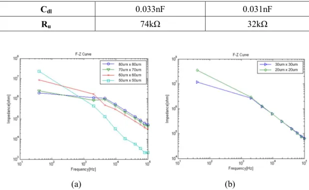
In the measurement of retina interface impedance, one end of the probe of impedance analyzer was fixed at column 1 of the wire-bonded recorder as the other end moved from column 2 to column 15 to measure interface impedances of different electrode distances. Experiments were done on row A to row H to measure the impedance of multi sizes of electrodes. Frequency bandwidth was between 40Hz and 100kHz with 201 recording points. AC signal was sine wave with 500 mV magnitude, and no DC bias potential was included. The measurement results of frequency to impedance curve are shown in Fig. 2.6. Randomly choose data number 1, 5, 10, 20, 40, 80, 120, 160 and 201 totally 9 points from the recorded points. Frequency and impedance axes are in logarithm scale. Figure 2.6(a) shows the impedance between column 1 and column 6 of the big electrode chip; Fig. 2.6(b) shows the impedance between column 1 and column 7 of the small electrode chip. In each figure, the smaller electrodes have larger impedance at low frequency. But 10-μm and 40-μm side length electrodes did not yield consistent results, so these sizes were not included in Fig. 2.6(b). The impedance of small electrode sets was not always larger than big electrode sets, because these two kinds of sets were separated into two chips. Therefore, in the following analysis, we studied the results of big electrode chip only. Besides the impedance between column 1 and column 2 and between column 1 and column 15 of the big electrode chip, other columns yielded consistent results, so these columns were not included in further analysis. These problems may come from that retina did not and very closely attach to the chip thus the measurement results were not very reliable at the two ends of microelectrode chip. In this case, large contact resistance (Rco) was shown in the retina interface that would disturb the measurement
results.
Looking into the relationship between retina interface impedance and electrode distance, we compared the relationship of row C at low frequency and at high frequency. Figure 2.7(a) shows the electrode distance to impedance curve at low frequency (40Hz, 0.5kHz, 1kHz and 1.5kHz); Fig. 2.7(b) shows the electrode distance to impedance curve at high frequency (25kHz, 50kHz, 75kHz and 100kHz). No consistent electrode distance to impedance relationship at low frequency, whereas impedance increases with increasing electrode distance at high frequency. These results indicate that the impedance modulus is not highly dependent on Rco at high