Surface potential and magnetic properties of La
0.7Sr
0.3MnO
3periodic arrays
fabricated by direct electron beam writing
Ming-Chung Wu,1,a兲 Yi-Jen Wu,1Yu-Ching Huang,1Chih-Min Chuang,1
Kuo-Chung Cheng,2Ching-Fuh Lin,3Yang-Fang Chen,4,5,a兲and Wei-Fang Su1,5,b兲 1
Department of Materials Science and Engineering, National Taiwan University, Taipei 106-17, Taiwan 2Department of Chemical Engineering and Biotechnology, National Taipei University of Technology, Taipei 106-08, Taiwan
3Graduate Institute of Electro-optical Engineering and Department of Electrical Engineering, National Taiwan University, Taipei 106-17, Taiwan
4Department of Physics, National Taiwan University, Taipei 106-17, Taiwan
5Center for Condensed Matter Sciences, National Taiwan University, Taipei 106-17, Taiwan 共Received 4 April 2008; accepted 18 May 2008; published online 29 July 2008兲
It is demonstrated that magnetic periodic arrays can be easily fabricated from direct writing water developable La0.7Sr0.3MnO3electron beam resist. Two unique features of our approach are共1兲 the patterned La0.7Sr0.3MnO3resist film can be developed using nontoxic and environmentally friendly pure water and共2兲 either positive or negative patterns can be fabricated depending on the dosage of electron beam. The mechanism of the dual function characteristic of the resist was studied using Kelvin probe microscope. The surface potential of patterned La0.7Sr0.3MnO3 resist increases with increasing electron beam dosage due to the changes of resist composition. The formations of periodic magnetic arrays were confirmed by the studies of scanning electron microscope and magnetic force microscope. The magnetization of La0.7Sr0.3MnO3can be enhanced by postsintering the sample at 900 ° C after electron beam irradiation. We have therefore provided a one-step, simple, and convenient alternative technique for the fabrication of nanoscale magnetic patterns, which form the building blocks for the study of physical properties in periodic magnetic arrays. © 2008
American Institute of Physics.关DOI:10.1063/1.2957489兴
I. INTRODUCTION
Electron beam lithography is a technique to generate pat-terns on a surface using a beam of electrons. Although the pattern generating rate may appear not as fast as a parallel technique like photolithography, electron beam lithographic pattern can easily reach the nanoscale regime by controlling the electron beam width and can overcome the diffraction limit of light source.1,2 Resists are usually passive and have no specific function. If one can develop resists with active functions such as conductivity, luminescence, and magnetic properties, the fabrication process of specific devices can be simplified. However, relatively few active resists are re-ported. Clendennings et al.3 and Maclachlan et al.4reported a direct writing of patterned ceramics using electron beam lithography and Co-PFS resist, and the resist could be used in spintronics as an isolating magnetic layer in a nanogranu-lar in-gap structure. Pang et al.5presented a method to pro-duce a luminescent resist, polymethyl methacrylate 共PMMA兲-quantum-dot 共QD兲 composite, by prepolymerized PMMA and colloidal semiconductor QDs. Song et al.6 re-ported in 2005 a nanoengineered fluorescent response from an active resist semiconductor core shell 共CdSe/ZnS兲 QDs being close to the surface plasmon polariton field of the pe-riodic Ag arrays. Saifullah et al.7demonstrated a fabrication
of high aspect ratio ZnO structure by electron beam lithog-raphy, and the best photoluminescence characteristics of ZnO was exhibited after heat treated at 500 ° C.
Recently, we have developed a water developable La0.7Sr0.3MnO3 electron beam resist,8 which can be used to fabricate either positive or negative magnetic nanopatterns in one step. In this paper, we have further studied their surface potential behaviors using Kelvin probe force microscope 共KFM兲 and magnetic properties of La0.7Sr0.3MnO3 nanopat-terns using magnetic force microscope 共MFM兲. For MFM, nanoscale magnetic patterns9,10 or current flow distributions11 can be profiled through the interaction be-tween a magnetized tip and the sample surface. Moreover, for KFM, one can detect the surface potential from the work function difference between a noble metal-coated tip and the surface of materials and obtain the work function in an indi-rect way.12–15The results of the surface potential of patterned La0.7Sr0.3MnO3 by KFM confirm the mechanism of dual functional characteristics of the resist. The magnetic proper-ties of the structure can be clearly detected by MFM. Our approach provides a simple and convenient alternative tech-nique for the fabrication of nanoscale magnetic patterns, which form the building blocks for the study of physical properties in periodic magnetic array.
II. EXPERIMENTAL DETAILS
In this experiment, the electron beam resist was prepared by dissolving 4.50 wt % of lanthanum nitrate 关La共NO3兲3· 6H2O, Acros, 98%兴, strontium hydroxide a兲Electronic mail:[email protected].
b兲Electronic mail: [email protected].
JOURNAL OF APPLIED PHYSICS 104, 024517共2008兲
关Sr共NO3兲2, Riedel–deHaen, p.a.兴, manganese nitrates 关Mn共NO3兲2· 4H2O, Fluka,⬎97%兴, and 1.70 wt % polyvinyl alcohol共PVA兲 共Acros, 88%, 22 000 g/mol兲 in water with a molar ratio of La: Sr: Mn= 0.7: 0.3: 1. The solution was stirred for 48 h at 25 ° C. Then the La0.7Sr0.3MnO3material was spin coated at 3000 rpm for 90 s to give a nominal thickness of about 180 nm. High-resolution nanolithography was performed by writing specific patterns across the 150 m field with a 2.5 nm beam step size using a Hitachi ELS-7500EX machine operating at 100 kV with a probe cur-rent of 1.0 nA. A sample containing a 3⫻3 array of field was exposed with a start dose of 1 s then with an additional dose increments of 0.01, 0.1, and 1 s per field, respec-tively. The exposed sample was then developed with pure water for 30 s. The patterned La0.7Sr0.3MnO3 samples were measured by atomic force microscopy 共AFM兲 共Digital In-struments, Dimension-3100 Multimode兲 for surface mor-phology and roughness, and the microstructures of the samples were observed by field emission scanning electron microscope共Elionix, ERA-8800FE, Japan兲. The
magnetore-sistance properties and magnetic properties were measured by physical property measurement system共Quantum Design, PPMS-9兲 and superconducting quantum interference devices 共SQUID兲 共Quantum Design, MPMS-XL7兲, respectively. The surface potential and magnetic behavior distribution of the patterned La0.7Sr0.3MnO3 were evaluated using KFM and MFM共Digital Instruments, Dimension-3100 Multimode兲.
III. RESULTS AND DISCUSSION
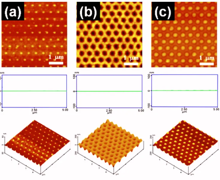
We have demonstrated that the water developable La0.7Sr0.3MnO3 electron beam resist exhibits dual negative and positive patterning functions depending on the electron beam dosage. Figures 1共a兲–1共c兲 are the two dimensional AFM images, cross-section images, and three dimensional AFM images of the La0.7Sr0.3MnO3 periodic arrays on sili-con wafer substrate fabricated using different electron beam dosages. Figure1共a兲is a negative pattern obtained at a low electron beam dose of 3.2 mC/cm2. Figure1共b兲is a positive pattern obtained at a medium electron beam dose of FIG. 1. 共Color online兲 Two dimensional and three dimensional AFM topographic images and cross-section images of La0.7Sr0.3MnO3periodic arrays.共a兲 Negative La0.7Sr0.3MnO3periodical structure with low dosage共3.2 mC/cm2兲 electron beam irradiation. 共b兲 Positive La0.7Sr0.3MnO3periodical structure with medium dosage共32.0 mC/cm2兲 electron beam irradiation. 共c兲 Negative La0.7Sr
0.3MnO3periodical structure with high dosage共233.6 mC/cm2兲 electron beam irradiation. The scan size is 5⫻5 m2.
32 mC/cm2. At a high electron dose of 233.6 mC/cm2, we obtained a negative pattern again. Although the dose of the exposure of this La0.7Sr0.3MnO3 resist is relatively high in comparison to most organic resists, the La0.7Sr0.3MnO3resist generates active electromagnetic functional nanopatterns in one step, whereas the use of conventional organic resists to generate La0.7Sr0.3MnO3 patterns involves three steps: 共1兲 fabricate patterns from organic resist, 共2兲 deposit La0.7Sr0.3MnO3 on the patterns, and 共3兲 remove organic re-sist. The use of La0.7Sr0.3MnO3electron beam resist will not only reduce process steps but also use no environmental harmful organic chemicals as compared to the organic resist. Our La0.7Sr0.3MnO3 resist exhibits zwitterresist characteris-tics, so the height or depth in different patterns will vary with electron dose. The height of regular honeycomb array of La0.7Sr0.3MnO3pillars关Fig.1共a兲兴 is 10 nm, and the depth of positive pattern of regular honeycomb array is 50 nm 关Fig. 1共b兲兴. Finally, the height of regular honeycomb array of La0.7Sr0.3MnO3pillars 关Fig.1共a兲兴 is 40 nm.
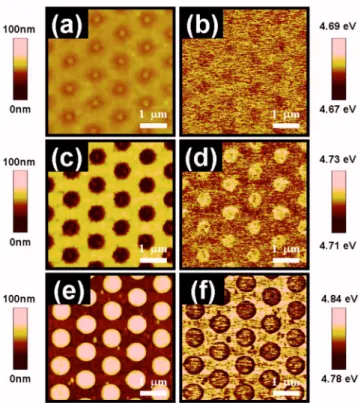
We have previously illustrated that the formation of La0.7Sr0.3MnO3resist pattern is due to the heat from the elec-tron beam exposure. Herein, we measure the surface poten-tial of different La0.7Sr0.3MnO3patterns by KFM to confirm the formation of La0.7Sr0.3MnO3 resist pattern. KFM has been widely used for the nanoscale mapping of surface po-tential differences and local dipoles that reveal important in-formation on material properties. At the low electron dose 共2.8 mC/cm2兲, only the exposed area is affected by the cross-linking of the PVA and results in a negative pattern of regular honeycomb array of La0.7Sr0.3MnO3 pillars. At the low electron dose, the surface potential of the La0.7Sr0.3MnO3 pillars consisting of nitrate salt and PVA is about 4.68 eV. At the medium dose共28.8 mC/cm2兲, the ni-trate salt components of La0.7Sr0.3MnO3resist react with the PVA at the exposure area关Figs.2共c兲and2共d兲兴. An explosive reaction occurs, the so-called autoignited combustion,16–18 and then the resist structure will change to form loose par-ticles that can be easily removed by water to form positive pattern of regular triangular array关Figs.2共c兲and2共d兲兴. The surface potential of the La0.7Sr0.3MnO3positive patterns con-sisting of nitrate salt and PVA at the medium dose is about 4.72 eV. The surface potential of the La0.7Sr0.3MnO3periodic array at medium dose 共4.72 eV兲 is similar to the surface potential of periodic array at low dose共4.68 eV兲 because the chemical compositions of La0.7Sr0.3MnO3 patterns at low or medium dose are similar. Finally, at the high dose 共224 mC/cm2兲, the area exposed to the electron beam 关Figs. 2共e兲and2共f兲兴 shows a negative pattern with the formation of crystalline La0.7Sr0.3MnO3. At or above this electron beam thermal energy threshold, the pure phase of La0.7Sr0.3MnO3 formed as a solid pattern; the neighboring loose La0.7Sr0.3MnO3 particle can be removed by water. The sur-face potential of the La0.7Sr0.3MnO3 positive patterns at the high dose is about 4.80 eV, which is the same as the value reported in the literature.19–23
Figure3reveals x-ray diffraction共XRD兲 patterns of the La0.7Sr0.3MnO3 thin film sample sintered at different tem-peratures. All the peaks can be perfectly indexed as the pure rhombohedral phase关R3¯c共167兲兴 共Ref.24兲 of La0.7Sr0.3MnO3
with lattice constants a = 5.09 Å and c = 13.37 Å. The sample sintered at 300 ° C clearly indicates the formation of high symmetry pseudocubic phase of La共Sr兲MnO3 contain-ing trace amounts of MnO2and La2O3impurity phases. The sample sintered at 900 ° C indicates the change from impu-rity phase to a rhombohedral form of the pervoskitelike structure. Therefore, the patterned La0.7Sr0.3MnO3 was postsintered at 900 ° C to obtain the pure rhombohedral phase for high magnetic susceptibility.
FIG. 2.共Color online兲 Topographic images 共a, c, e兲 and KFM images 共b, d, f兲 of La0.7Sr0.3MnO3periodic arrays.共a,b兲 Negative La0.7Sr0.3MnO3 periodi-cal structure with low dosage共2.8 mC/cm2兲 electron beam irradiation. 共c,d兲 Positive La0.7Sr0.3MnO3 periodical structure with medium dosage 共28.8 mC/cm2兲 electron beam irradiation. 共e,f兲 Negative La0.7Sr
0.3MnO3 pe-riodical structure with high dosage共224.0 mC/cm2兲 electron beam irradia-tion. The scan size is 5⫻5 m2.
FIG. 3. 共Color online兲 XRD patterns of water developable La0.7Sr0.3MnO3 electron beam resist material sintered at different temperatures for 4 h.
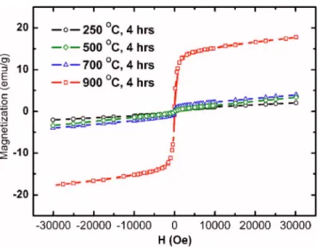
The La0.7Sr0.3MnO3 powders sintered at different tem-peratures were measured by SQUID at 300 K, as shown in Fig. 4. The magnetization of La0.7Sr0.3MnO3 powders sin-tered at 250, 500, and 700 ° C almost have the similar satu-ration magnetization value of ⫾3 emu/g at saturated mag-netic susceptibility under 30 000 Oe at 300 K. However, the La0.7Sr0.3MnO3 powder sample sintered at 900 ° C exhibits saturation the magnetization of ⫾18 emu/g at saturated magnetic susceptibility under 30 000 Oe at 300 K. This shows that the magnetization of La0.7Sr0.3MnO3at saturated magnetic susceptibility changes with different sintering tem-peratures. Moreover, the differences of saturation magnetiza-tion of La0.7Sr0.3MnO3 at saturated magnetic susceptibility are because of the formation of pure La0.7Sr0.3MnO3 crystal-line phase. The La0.7Sr0.3MnO3 powder sample sintered at 900 ° C for 4 h exhibits the highest magnetization among all the powder samples at saturated magnetic susceptibility be-cause the sample forms a pure La0.7Sr0.3MnO3 crystalline phase.
The magnetoresistance properties of the water develop-able La0.7Sr0.3MnO3 resist were studied for powdered samples because the electron beam samples were too small to be studied by SQUID. The powder was prepared by dry-ing the resist material at 120 ° C for 12 h and sintered at 900 ° C for 4 h. The magnetoresistance properties of the re-sist material were studied at different temperatures and dif-ferent magnetic fields as shown in Figs. 5共a兲and5共b兲. The water developable La0.7Sr0.3MnO3material exhibits negative magnetoresistance effects. The resistance of the material de-creases inversely with the external magnetic field and in-creases as the temperature inin-creases up to 250 K. However, the resistance 共⍀兲 at low temperature 共⬃25 K兲 increases slightly due to the Coulomb barriers that exist on the grain boundary, hindering electron transport.
Figures 6共a兲 and 6共b兲 show scanning electron micros-copy 共SEM兲 images of La0.7Sr0.3MnO3 material exposed to an electron beam followed by 4 h of sintering at 900 ° C, which produces a honeycomb style periodic pattern, with their lattice constants of 600 nm. The La0.7Sr0.3MnO3
mate-rial exhibits positive resist characteristic 关Fig. 6共a兲兴 and negative resist characteristic关Fig.6共b兲兴. Figure6共c兲shows a SEM image of La0.7Sr0.3MnO3 material sintered at 900 ° C for 4 h with a square periodic pattern and positive resist characteristic, and its lattice constant is 400 nm. The sample patterns remain despite being post-treated at high tempera-ture. These results illustrate the dual functional characteristic of water developable La0.7Sr0.3MnO3materials and its capa-bility to be either positive or negative by varying the electron doses. Figure 6共d兲 shows the energy dispersive x-ray spec-troscopy共EDS兲 analysis of the patterned La0.7Sr0.3MnO3 ma-terial sintered at 900 ° C for 4 h. The atomic ratio of La, Sr, and Mn is approximately 0.7:0.3:1.0. This result indicates that the fabrication process does not alter the initial reac-tants’ mixing ratio.
The nanoscale magnetic properties of water developable La0.7Sr0.3MnO3electron beam resist material were studied by MFM. MFM equips a scanning probe microscope that can map the spatial distribution of magnetism by measuring the magnetic interaction between a sample and a tip. Figure 7 共a⬃ j兲 shows AFM topographic images and magnetic force FIG. 4. 共Color online兲 The hysteresis curves of water developable
La0.7Sr0.3MnO3electron beam resist material sintered at different tempera-tures for 4 h are measured under 30 000 Oe at 300 K.
FIG. 5. 共Color online兲 The magnetoresistance properties of water develop-able La0.7Sr0.3MnO3electron beam resist material sintered at 900 ° C for 4 h are measured under 30 000 Oe at 300 K.共a兲 The relationship between re-sistance and temperature at various magnetic fields and共b兲 the relationship between the magnetoresistance ratio and temperature at various magnetic fields.
gradient images共phase signal兲 of the samples. These images are 2⫻5 m2, and their data scales are 100 nm and 20°, respectively. In MFM mode, the cantilever is lifted up 25 nm higher than in the topography mode. Figures 7共a兲 and7共b兲 illustrate the topographic image and magnetic force gradient image of a sample with regular triangular pillar array 共600 nm in diameter, 1.0 m lattice constant, and 50 nm thick兲. The sample was produced by exposing the resist to an elec-tron dose of 224.0 mC/cm2without postsintering treatment. Figures7共c兲and7共d兲,7共e兲and7共f兲, and7共g兲 and7共h兲 show the regular triangular La0.7Sr0.3MnO3 pillar array sintered at 300, 500, and 700 ° C for 4 h, respectively. For the samples postsintered at 300, 500, 700 ° C, the sizes of La0.7Sr0.3MnO3 pillar array decrease slightly with the increasing postsinter-ing temperature, and the MFM phase shift signals are be-coming obscure. The result indicates that MFM contrasts come from the atomic force distribution in the samples rather than the magnetic force distribution for these samples sin-tered below 700 ° C. However, the La0.7Sr0.3MnO3pillar ar-ray with postsintering at 900 ° C for 4 h shows clear MFM signals; it indicates that MFM images are due to the mag-netic force distribution in the sample rather than the atomic force. From the data presented, it can be derived that the MFM behavior of La0.7Sr0.3MnO3 array occurred due to the formation of pure La0.7Sr0.3MnO3 crystalline phase. The finding also corresponds to the previous XRD and SQUID study.
To further confirm that the MFM images are indeed ow-ing to the magnetic force distribution instead of van der Waals forces, we performed various MFM measurements by changing the tip-sample separation distance 共lift scan height兲. The principle of MFM measurement is based on
noncontact AFM. Therefore, both the atomic force and the magnetic interactions are detected. From the aspect of atomic force, neutral atoms and molecules are subject to two distinct forces correlating to large and short distances. The attractive force is at long ranges and a repulsive force is at short ranges. The Lennard-Jones25potential is a simple mathemati-cal model that represents this behavior as 关Eq.共1兲兴
V共r兲 = 4
冋
冉
r冊
12 −冉
r冊
6册
, 共1兲where is the depth of the potential well, r is the distance between two neutral atoms or two molecules, and is the finite distance at which the potential is zero. These param-eters can be fitted to reproduce experimental data or deduced from the results of accurate quantum chemistry calculations. The term 共1/r兲12 describes repulsion and the term 共1/r兲6 describes attraction. The force function is the negative of the gradient of the above potential, which is given by
F共r兲 = − d drV共r兲rˆ = 4
冋
12 12 r13 − 6 6 r7册
rˆ. 共2兲The magnetic force equation between two poles abides by Coulomb’s law and follows
FIG. 6. SEM images of La0.7Sr0.3MnO3periodic arrays exposed to the elec-tron beam plus 4 h sintering at 900 ° C. 共a兲 Honeycomb periodic pattern with positive resist characteristic, 共b兲 honeycomb periodic pattern with negative resist characteristic,共c兲 square periodic pattern with positive resist characteristic, and共d兲 EDS analysis of the patterned La0.7Sr0.3MnO3material sintered at 900 ° C for 4 h, showing the presence of La, Sr, Mn, and O.
FIG. 7.共Color online兲 MFM images of La0.7Sr0.3MnO3periodic arrays.关共a兲 and共b兲兴 Topographic image and phase shift image, respectively, of sample prepared at 233.6 mC/cm2electron exposure plus postsintering with a tri-angular holes array with a 600 nm diameter, 1000 nm lattice constant, and 40 nm thickness,关共c兲 and 共d兲兴 after electron beam irradiation plus 300 °C postsintering, 关共e兲 and 共f兲兴 after electron beam irradiation plus 500 °C postsintering, 关共g兲 and 共h兲兴 after electron beam irradiation plus 700 °C postsintering, and关共i兲 and 共j兲兴 after electron beam irradiation plus 900 °C postsintering. The data scales of these images are 100 nm and 20°, respectively.
F = p1p2
40r2, 共3兲
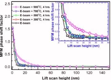
where r is the distance between two poles, p1 and p2 are poles, and0is the permeability of empty space that is equal to 4⫻10−7 Wb/A m. Thus, we can see that the van der Waals force decreases with increasing distance more rapidly than the magnetic force. Figure8shows the phase shift fac-tor, which is proportional to the force acting on the tip, at different tip-sample distances in the MFM and AFM mea-surements for the samples with different postsintering. The sample with post-900 ° C-sintering treatment exhibits a slow force that decreases with increasing tip-sample distance, in-dicating that the sample has a large magnetic moment. Whereas, the samples with post-low-sintering treatment 共⬍700 °C兲 or without postsintering treatment have negli-gible magnetic moment and exhibit a force that decreases drastically with increasing the tip-sample distance. At small tip-sample distances 共⬍⬍10 nm兲, the total force is domi-nated by the atomic force, and the difference between the MFM and AFM phase images is indistinguishable. When the distance is greater than 10 nm, the magnetic force becomes dominant. Both forces diminish after the distance exceeds 30 nm. The overall trend of two experimental curves is seen to be described quite well by Eqs. 共2兲 and 共3兲. We therefore conclude that a well-defined magnetic pattern has been fab-ricated using water developable La0.7Sr0.3MnO3 electron beam resist.
IV. CONCLUSIONS
In summary, we have created magnetic patterns using water developable La0.7Sr0.3MnO3electron beam resist in an environmentally friendly one-step method, and both positive and negative patterns are ready to be fabricated by only vary-ing electron dose. The surface potential of patterned La0.7Sr0.3MnO3measured by KFM is very useful to identify the chemical compositions and mechanism of the dual func-tion of La0.7Sr0.3MnO3resist. The magnetic properties of the
patterned La0.7Sr0.3MnO3can be clearly observed by postsin-tering the sample at 900 ° C for 4 h after electron beam writ-ing. We would like to stress that our study provides a simple and convenient approach for the fabrication of magnetic pat-terns, which underpin many interesting physical properties awaiting future explorations.
ACKNOWLEDGMENTS
Financial support obtained from the National Science Council of Taiwan 共Project Nos. NSC95-3114-P-002-003-MY3 and NSC96-2628-E-002-017-NSC95-3114-P-002-003-MY3兲 is highly appreci-ated. The authors also thank Professor C. H. Kuan, Professor C. W. Chen, Mr. Y. Y. Lin, Ms. S. Chen, and Mr. J. F. Lin of National Taiwan University for helpful discussions and Mr. A. J. Su of University of Pittsburgh for editing the manu-script. The electron beam lithography was carried out using the Elinox’s facility located in the National Taiwan Univer-sity Center for Information and Electronics Technologies.
1C. S. Wu, C. F. Lin, H. Y. Lin, C. L. Lee, and C. D. Chen,Adv. Mater.
共Weinheim, Ger.兲19, 3052共2007兲.
2H. Y. Lin, L. C. Tsai, P. Y. Chi, and C. D. Chen, Adv. Mater.共Weinheim, Ger.兲 18, 1517 共2006兲.
3S. B. Clendenning, S. Aouba, M. S. Rayat, D. Grozen, J. B. Sorge, P. M. Broderson, R. N. S. Sodhi, Z.-H. Lu, C. M. Yip, M. R. Freeman, H. E. Ruda, and I. Manners,Adv. Mater.共Weinheim, Ger.兲16, 215共2004兲. 4M. J. MacLachlan, M. Ginzburg, N. Coombs, T. W. Coyle, N. P. Raju, J.
E. Greedan, G. A. Ozin, and I. Manners,Science287, 1460共2000兲. 5L. Pang, Y. Shen, K. Tetz, and Y. Fainman,Opt. Express13, 44共2005兲. 6J. Song, T. Atay, S. Shi, H. Urabe, and A. V. Nurmikko,Nano Lett.5,
1557共2005兲.
7M. S. M. Saifullah, K. R. V. Subramanian, D.-J. Kang, D. Anderson, W. T. S. Huck, G. A. C. Jones, and M. E. Welland,Adv. Mater.共Weinheim, Ger.兲
17, 1757共2005兲.
8M. C. Wu, C. M. Chuang, Y. F. Chen, and W. F. Su,J. Mater. Chem.18, 780共2008兲.
9I. C. Chen, L. H. Chen, A. Gapin, S. Jin, L. Yuan, and S. H. Liou,
Nano-technology19, 075501共2008兲.
10H. Kuramochi, T. Uzumaki, M. Yasutake, A. Tanaka, H. Akinaga, and H. Yokoyama,Nanotechnology16, 24共2005兲.
11F. Král, D. Perednis, B. Huey, D. A. Bonnell, G. Kostorz, and L. J. Gauck-ler, Adv. Mater.共Weinheim, Ger.兲 10, 1442 共1998兲.
12H. Hoppe, T. Glatzel, M. Niggemann, A. Hinsch, M. C. Lux-Steiner, and N. S. Sariciftci,Nano Lett.5, 269共2005兲.
13H. O. Jacobs, P. Leuchtman, O. J. Homan, and A. Stemmer,J. Appl. Phys. 84, 1168共1998兲.
14Z. Yang and M. G. Spencer,Appl. Phys. Lett.89, 263504共2006兲. 15B. Pérez-García, J. Abad, A. Urbina, J. Colchero, and E. Palacios-Lidón,
Nanotechnology19, 065709共2008兲.
16H. B. Park, H. J. Kweon, Y. S. Hong, S. J. Kim, and K. Kim,J. Mater. Sci. 32, 57共1997兲.
17S. K. Behera, P. Barpanda, S. K. Pratihar, and S. Bhattacharyya,Mater.
Lett.58, 1451共2004兲.
18C. M. Chuang, M. C. Wu, Y. C. Huang, Y. F. Chen, C. F. Lin, and W. F. Su,Nanotechnology17, 4399共2006兲.
19T. Kudo, M. Tachiki, T. Kashiwai, and T. Kobayashi,Jpn. J. Appl. Phys.,
Part 237, L999共1998兲.
20S. Yunoki, A. Moreo, E. Dagotto, S. Okamoto, S. S. Kancharla, and A. Fujimori,Phys. Rev. B76, 064532共2007兲.
21I. Bergenti, V. Dediu, M. Murgia, A. Riminucci, G. Ruani, and C. Taliani,
J. Lumin.110, 384共2004兲.
22E. Arisi, I. Bergentia, V. Dediu, M. A. Loi, M. Muccini, M. Murgia, G. Ruani, C. Taliani, and R. Zamboni,J. Appl. Phys.93, 7682共2003兲. 23D. W. Reagor, S. Y. Lee, Y. Li, and Q. X. Jia,J. Appl. Phys.95, 7971
共2004兲.
24JCPDS Card No. 89-8098共2003兲
25J. E. Lennard-Jones,Proc. Phys. Soc. London43, 461共1931兲. FIG. 8. 共Color online兲 The phase shift factors of La0.7Sr0.3MnO3periodic