The Design and Simulations of Carrier Recovery Circuits with
Pre-assured 2
ndorder Digital Loop Filter
Chien-Hsing Liao
a, Fu-Hao Yeh
a, Tai-Kuo Woo
b,
and Fu-Nian Ku
a aProgram of Information Technology, Fooyin University, Taiwan (ROC)
bDepartment of Information Management, National Defense University, Taiwan (ROC)
Abstract —Carrier recovery circuit is always a crucial
issue in circuit designs, especially in mobile
communications and many other applications which will produce phase shift or frequency drift due to relative activity or environments variations. For keeping track of these crucial changing parameters, a synchronization circuit with 2nd order digital loop is generally applied for its simplicity, flexibility, and fast settling time. In this paper, a typical second order digital loop filter with pre-assured stable convergence triangle from Jury criteria is developed, which can then be directly applied in many circuit designs with phase or frequency drifts by simply adjusting two digital loop parameters. The convergence property and the effectiveness of this digital loop filter and its applied circuits with derived recursive formulations are well studied and simulated. This simple and direct scheme can easily tell the designers the stable convergence contours under specific circumstances in the whole design stages.
I. INTRODUCTION
The importance of synchronization circuits in modern circuit designs is indisputable and is always a crucial issue in circuit designs, especially in mobile communications and many applications which will produce phase shift or frequency drift due to relative activity, components aging, or environments variations. Therefore, a fast, stable, and flexible tracking loop design is always a necessity. For example, the Doppler effects will be generated while the systems are in relatively mobile conditions. And it will be much more severe, especially when the systems are operating in higher frequency bands, e.g., a few kHz drift will be normal for Ku-band satellite communications. In addition, the inherent frequency variations of crystal oscillator no less than 10 ppm in the whole operating frequency band and temperature range due to components aging and environments are generally happened, which will cause relatively large phase shift or frequency drift if a specific synchronization circuit is not applied. Furthermore, if sophisticated spread spectrum communications, e.g., fast frequency hopping, is considered, a synchronization circuit with fast and stable convergence performance has to be made for achieving the specified hopping performance.
Conventionally, the most well known synchronization loop design is analog phase lock loop (PLL) with added voltage controlled oscillator (VCO) and loop filter, or with direct digital synthesizer (DDS) [1-5]. But, nowadays, full
digital PLL design methods and approaches with digital loop filters are also applied in many related fields for its inherent benefits [4]. The use of higher-order digital loop filter should generally be restricted to filtering purpose, as these designs can be slower than lower-order PLLs and may exhibit a lower phase margin. And if a fast-settling PLL application is desired, e.g., a fast frequency hopping circuit, it is appropriate to select a lower-order digital loop for its simplicity and flexibility [8-10]. The theoretic analysis and design of a PLL circuit is complicated, therefore, many design approaches based on some specific models or simulation tools are taken to evaluate system parameters in a fast manner [14-15] [6-7].
In this paper, a simple and direct scheme based on a pre-assured stable 2nd order digital loop filter for designing a carrier recovery circuit is developed, which can tell the designer the convergence area by simply adjusting or selecting two loop parameters in the whole design stages.
The remainder of this paper is organized as follows. In Section II, the basics for a pre-assured stable 2nd order digital loop design will be addressed thoroughly, which include its function block diagram, recursive formulations, transfer function, and convergence characteristics and responses with two simply adjusted parameters. In Section III and IV, two typical application cases with pre-assured stable 2nd order digital loop design, i.e., QPSK phase tracking and Radio frequency tracking, respectively, will be presented. Conclusion is in final Section V.
II. PRE-ASSURED 2ND
ORDER DIGITAL LOOP FILTER In this section, the function block diagram, recursive formulations, transfer function, and convergence triangle and response for a pure 2nd order digital loop filter design are addressed.
A. Function Block Diagram
Fig. 1 shows a typical synchronization function block
diagram, which is consisted of the synchronization circuit and 2nd order digital loop filter with two adjustable C1 and C2
parameters. The synchronization circuit is labeled as f(x)=1 for analyzing the pure 2nd order digital loop filter only. The initial input signal δxm value is δx0=x0 and the feedback
signals within this function diagram are updated periodically by system clocks. The C1 and C2 are the only two parameters
which we can select to let δxmconverge to zero for a stable
response. In this diagram, two internal small feedback loops are built for generating Sm+1, xm+1, ym+1, and many other
parameters for recursive formulations. + + Z-1 C1 C2 Sm+1 xm+1 ym+1 δx0=x0 f(·) Z-1 + Sm ym
2nd Order Digital Loop Filter
Synchronization ckt
Fig. 1 The typical synchronization function block diagram with two
adjustable C1 and C2 parameters from 2nd order digital loop filter
B. Recursive Formulations
The basic recursive formulations are derived from (1a) to (1d), respectively, based on the two internal feedback loops from Fig. 1. 1 2 m m m S + =C ⋅
δ
x +S , (1a) 1 1 1 m m m x + =C ⋅δ
x +S +, (1b) 1 1 m m m y + = y +x + , (1c) 1 0 1 0 m m m m x x y x x yδ
+ =δ
− + ⇒δ
=δ
− , (1d) where δxm is the input difference quantity. Moreover, thetransfer function H(z) of this 2nd order digital loop filter with
f(x)=1 is derived and shown in (2) by wrapping up and taking z-transform of (1a) to (1d).
( )
(
)
(
)
(
)
2 2 0 1 2 1 1 2 1 m z x H z x z C C z Cδ
δ
− = = + + − ⋅ + − (2) C. Convergence TriangleThe pure 2nd order digital loop filter will be stable if C1
and C2 parameters in the denominator of the H(z) transfer
function could satisfy the constrained stable conditions from Jury criteria [11-12], which is represented as
1 2 1 2
0<C <2 C >0 2C +C >4 , (3) where these three different curves formed by C1 and C2
combinations will generate a convergence triangle. Fig. 2 shows this theoretic syable convergence triangle based on (3).
Convergence Triangle
Fig. 2 Theoretic stable convergence triangle based on Jury criteria (C1
is 0~2 and C2 is 0~4)
Within this constrained region, the arbitrary combinations of C1 and C2 parameters will generate stable system
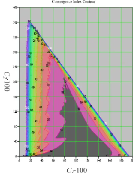
responses only with the differences of clock cycles required to achieve stable conditions. Fig. 3 shows the simulated convergence clock cycle contours with only 0.1% oscillating amplitude variations, i.e., the final amplitude variations to reach stable criteria is within 0.1%. If the combinations of C1
and C2 are in the inner contours, the clock time to reach
stable criteria is shorter, i.e., it will reach stable condition more quickly. On the contrary, in the outer contours, the clock time to reach stable criteria is longer.
We can choose any combinations of C1 and C2within this
region to have a specific stable response. For example, within the inner constrained contour (grey color), the convergence clock cycles no more than ten (10) are required to reach the stable criteria of only 0.1% amplitude variations. In the same manner, for the outer pink contour the convergence clock cycles required will be increased to no more than twenty (20) whenever any combinations of C1 and C2values within this contour are selected. Finally, near the
edges of this convergence triangle, the convergent clock cycles will be much more than one hundred (100) cycles, which means the convergence speed to reach the stable criteria of 0.1% amplitude variations will be even slower and more sensitive.
Convergence Index Contour
Fig. 3 Convergence clock cycle contour within 0.1% amplitude variations for stable criteria
D. Convergence Response
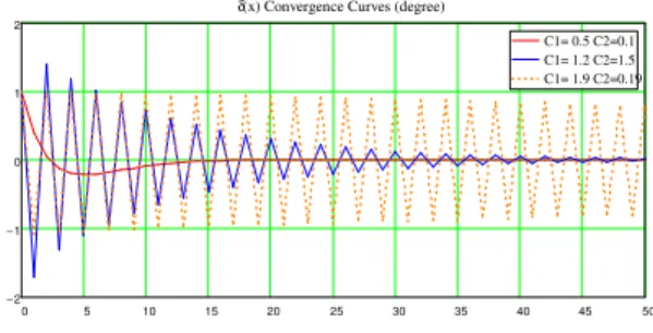
The δxmconvergence responses curves are shown in Fig. 4, where the x-axis represents the number of updating
clock cycles (m) and the y-axis represents the δxmamplitudes.
The first combination takes about ten cycles to be stable, and the second one take at least 50 cycles to be settled down. But when C1 and C2 are selected near the edges of convergence
triangle as shown in Fig. 2 or 3, e.g., C1= C2=0.19
combination, obviously it will need more clock cycles to converge or even become unstable if they are outside of this region. Therefore, the convergence speed simply depends on the choice of C1 and C2. If C1 and C2 are in the inner part of
the convergence triangle, it will converge more quickly; on the contrary, it will converge more slowly.
0 5 10 15 20 25 30 35 40 45 50 2 − 1 − 0 1 2 C1= 0.5 C2=0.1 C1= 1.2 C2=1.5 C1= 1.9 C2=0.19
δ(x) Convergence Curves (degree)
m
Fig. 4 Convergence response curves of 2nd order digital loop with three
adjustable C1 and C2 combinations
III. QPSK PHASE TRACKING WITH PHASE ROTATOR In this section, the function block diagram, recursive formulations, transfer function, and convergence response for a QPSK phase tracking circuit design are addressed.
A. Function Block Diagram
Fig. 5 shows the function block diagram of a QPSK phase
tracking circuit consisted of phase rotator, phase discriminator, and the pre-assured 2nd order digital loop filter. This is a typical phase tracking system, where the initial phase shift (θ0) and residue angular frequency (ωr) from
analog I and Q channel signals are mixed into this tracking system. The aim is, therefore, to correct the shifted signal phases by this tracking system. When this tracking loop works, the phase differences δθ will cause the phase rotator to rotate, and the two phase rotated signals J and P dependent on δθ values in each clock cycle will be input to the phase discriminator for a discriminated phase output. Thereafter, the two adjustable parameters C1 and C2 inside
the pre-assured 2nd order digital loop filter are taken for a stable output performance according to the specified convergence triangle as aforementioned. The phase rotator can be implemented with SRAM chips or a FPGA chip in a table look-up style.
Fig. 5 Function block diagram of QPSK phase tracking circuit with
phase rotator
B. Recursive Formulations
The basic recursive formulations based on Fig. 1 and Fig.
5 are derived from (3a) to (3d), respectively.
(
)
1 2 m p m m S + =C ⋅k fδθ
+S , (3a)(
)
1 1 1 m p m m x + =C k f⋅δθ
+S + , (3b) 1 1 m m m y + =y +x + , (3c)(
0)
m rmT ymδθ
=θ
+δω
− , (3d) where kp is the approximated slope for linear phasediscriminator output response; δθmis the mth phase tracking
error; f(δθm) is phase discriminated output represented and
approximated as (4) and (5), respectively [13].
(
m)
(
m)
sgn(
(
m)
)
(
m)
sgn(
(
m)
)
fδθ
=Jδθ
Pδθ
−Pδθ
Jδθ
(4)(
)
mod , 2 4 2 2 m m m fπ
δθ
π
δθ
δθ
π
π
+ = − (5)Fig. 6 shows the real phase discriminator characteristic
curve (red solid) and approximated curve (blue dashed) with
kp slope, where 8 2 p k
π
= ⋅. This is basically a saw-tooth waveform with π/2 phase cycle. For no loss of generality, if |I |=|Q|=1 is assumed, it will be available for each possible case from (5) when QPSK constellations are considered.
2 − −1.5 −1 −0.5 0 0.5 1 1.5 2 1.5 − 1 − 0.5 − 0 0.5 1 1.5
Phase Detector Characteristic Curves
θ/ 0.5π
Fig. 6 Phase discriminator characteristic curves (red solid: real; blue dashed: approximated)
C. Convergence Response
Fig. 7 shows three different δθmconvergence response
curves by selecting three C1 and C2 combinations for QPSK
phase tracking loop with residue frequency equal to -0.01 clock rate and initial phase of 135 degrees. The first combination takes about twenty cycles to be stable, and the second one take less than 10 cycles to be settled down. The third combination takes about at least 100 cycles to be within the specified 0.1% amplitude variations. The only convergence limitation is to keep the swing within a stable region, and it is always possible.
0 10 20 30 40 50 60 70 80 90 100 120 140 160 180 200 220 240 C1= 0.5 C2=0.1 C1= 1.2 C2=0.85 C1= 1.9 C2=0.15 δ(θ) Convergence Curves (degree)
m
Fig. 7 Convergence response curves for QPSK phase tracking loop
IV. RADIO FREQUENCY TRACKING WITH DDS
In this section, the function block diagram, recursive formulations, transfer function, and convergence response for a radio frequency tracking circuit design are addressed.
A. Function Block Diagram
Fig. 8 shows the function block diagram of a RF
frequency tracking loop with DDS (direct digital synthesizer). This is a typical frequency tracking system, where the phase shift and residue angular frequency (ωr) from analog I and Q
channels are mixed into this tracking system. θ0 is initial
phase shift assumed and δωT the phase tracking error in each clock cycle when this tracking loop works. The DDS output is the reference frequency of a synthesizer for even higher local frequency, i.e., if the reference frequency is fr, the
synthesizer frequency is N fr= fl . J and P are the two phase
shifted signals dependent on δωT values in each clock cycle. The input signal is radio frequency, its carrier is frf, the local
angular frequency of demodulator is fl, and δω = 2π(frf–fl),
the aim of this circuit is to make δω=0 by changing fl from
DDS synthesizer output. The aim is then to correct the drifted signal frequencies by this tracking system consisted of DDS, A/D and demodulator, phase discriminator, and the pre-assured 2nd order digital loop filter.
Fig. 8 Function block diagram of RF frequency tracking circuit with
DDS
B. Recursive Formulations
The basic recursive formulations based on Fig. 1 and
Fig. 8 are derived from (6a) to (6d), respectively.
(
)
1 2 m d p m m S + =C ⋅Nk k fδω
T +S , (6a)(
)
1 1 1 m d p m m x + =C Nk k f⋅δω
T +S + , (6b) 1 m m mTθ
+ =θ
+δω
, (6c) 1 0 1 m kd xmδω
+ =δω
− ⋅ + , (6d)where kd is function of DDS clock frequency and phase
register setting resolution, shown as fc/2P (P is register
resolution); kp is the approximated slope for linear phase
discriminator output response; N fr= fl. C. Convergence Response
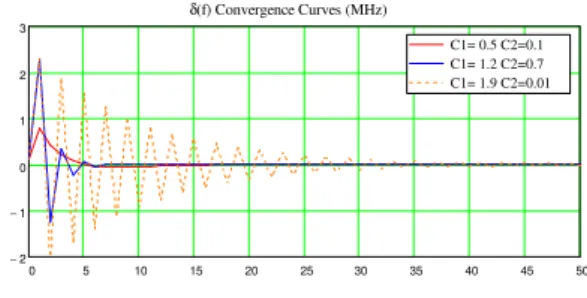
Fig. 9 shows three δfm convergence response curves (in
units of MHz) of Radio frequency tracking loop by setting residue frequency equal to 1% clock rate and initial phase equal to 135 degrees. The assumed update frequency 1/T is 10MHz. These three combinations take at most forty cycles to be settled down within the specified 0.1% amplitude variations. 0 5 10 15 20 25 30 35 40 45 50 2 − 1 − 0 1 2 3 C1= 0.5 C2=0.1 C1= 1.2 C2=0.7 C1= 1.9 C2=0.01 δ(f) Convergence Curves (MHz) m
Fig. 9 Convergence response curve of RF frequency tracking circuit with three adjustable C1 and C2 combinations
V. CONCLUSION
In this paper, a pre-assured 2nd order digital loop filter with easily adjustable parameters for predicted stable convergence characteristics and responses is proposed. Moreover, the general recursive formulations and derived convergence triangle for the filter itself and its applications in phase and frequency variations are also presented. This simple and direct scheme can tell the designers the convergence regions by simply adjusting or selecting these parameter combinations in the whole design stages.
REFERENCES
[1] A. Carlosena and A. Mánuel-Lázaro, “Design of High-Order Phase-Lock Loops”, IEEE Transactions on Circuits and Systems II: Express Briefs, vol. 54 , issue 1, pp. 9-13, 2007.
[2] X. Hongbing, G. Peiyuan, and L. Shiyi, “Modeling and Simulation of Higher-Order PLL Rotation Tracking System in GNSS Receiver”,
Proc. of ICMA 2009, pp. 1128-1133, 2009.
[3] C. Huang, L.-X. Ren, M. E.-K. Mao, and P.-K. He, “A Systematic Frequency Planning Method in Direct Digital Synthesizer (DDS) design”, WCSP’09, pp.1-4, 2009.
[4] B. Vezant, C. Mansuy, H. T. Bui, and F.-R. Boyer, “Direct Digital Synthesis-Based All-digital Phase-Locked Loop”, Joint IEEE
NEWCAS-TAISA '09, pp.1-4, 2009.
[5] S. Krazet and T. Bigg, “PLL Hardware Design and Software Simulation”, IEE Colloq. on Advanced Signal Processing for
Microwave Applications, pp. 7/1-7/11, 1996.
[6] J. Bruzdzinski, J. Gronicz, L. Aaltonen, and K. Halonen, “Behavioral Simulation of Fractional-N PLL Frequency Synthesizer: Phase Approach”, BEC 2008, pp. 121-124, 2008.
[7] M. Kozak and E. G. Friedman, “Design and Simulation of Fractional-N PLL Frequency Synthesizers”, Proc. of ISCAS’04, vol. 4, pp. IV-780-3, 2004.
[8] J. Stensby, “An Approximation of the Pull-Out Frequency Parameter in a Second-Order PLL”, Proc. of SSST '06, pp. 75-79, 2006. [9] J. Wang, “A Second-order Delay-Locked Loop of a Spread Spectrum
Receiver”, Proc. of MILCOM’93, vol. 3, pp. 809-813, 1993. [10] C. Chie, “A Second-Order Frequency-Aided Digital Phase-Locked
Loop for Doppler Rate Tracking”, IEEE Transactions on
Communications, vol. 28, issue 8, Part: 2, pp. 1431-1436, 1980.
[11] S. Zhaoqing; G. Xiaojun, and H. Yun'an, “A Nonregular Case of the Jury Test”, Proc. of the 3rd World Congress on Intelligent Control
and Automation, vol.4, pp. 2832 – 2834, 2000.
[12] L. H. Keel and S. P. Bhattacharyya , “A New Proof of the Jury Test”,
Proc. of the American Control Conference, pp. 3694-3698, Jun. 1998.
[13] C. Heegard, J. A. Hellerand and A.J. Viterbi. “A Microprocessor Based PSK Modem for Packet Transmission Over Satellite Channels”,
IEEE Tran. Com-26, no.5, p563, 1978.
[14] Bernard Sklar, Digital Communications, Prentice- Hall, 2nd Ed, pp.598-655, 2001.
[15] T. T. Ha, Digital satellite Communications, 2nd Ed., McGraw-Hill, pp.