Far-Field and Near-Field Distribution of GaN-Based
Photonic Crystal LEDs With Guided Mode Extraction
Chun-Feng Lai, Jim-Yong Chi, Senior Member, IEEE, Hao-Chung Kuo, Member, IEEE, Hsi-Hsuan Yen,
Chia-En Lee, Chia-Hsin Chao, Wen-Yung Yeh, and Tien-Chang Lu
Abstract—The near-field and far-field distribution of GaN LEDs with square photonic crystal (PhC) lattice are experimentally inves-tigated. The optical images of the near-field pattern are obtained from the guided electroluminescent light generated at the cen-ter of a special annular structure. For increasing lattice constant, symmetric patterns with varying number of petals according to the symmetry of the PhC are observed. The far-field distribution is studied with GaN-based film-transferred PhC LEDs with the thickness about 1500 nm. Angular-resolved measurements under electrical injection revealed guided modes extraction behavior and polarization based on the Bragg’s diffraction with the PhC lat-tice. Good agreement with the two-dimension free photon band structure is obtained.
Index Terms—GaN, LEDs, photonic crystal (PhC). I. INTRODUCTION
T
HROUGH the Bragg diffraction with the photonic crys-tal (PhC), guided light in PhC LED chips can escape from the deleterious trapping effects due to total internal re-flection [1]–[7]. Aperiodic PhC patterns have been reported for isotropic light extraction [6]. For controlling the collimation and polarization properties, periodic PhC with anisotropic light extraction has also been reported [4], [5], [8]. In this study, a de-tailed investigation was conducted to gain insights for the near-field and the far-near-field distribution of the guided mode extraction from the GaN-based PhC LEDs under electrical injection. A direct imaging approach is used for the in-plane angular distri-bution of the extracted light in the near field using an annular structure under electrical injection [2], [3]. The far-field patterns are investigated with the angular-resolved electroluminescence (EL) spectroscopy technique using a film-transferred LED struc-ture under the electrical injection. The experimental results are compared with the band structure calculation. In addition, an-gular distribution is also examined in the polarization-resolvedManuscript received November 30, 2008; revised December 22, 2008. First published June 12, 2009; current version published August 5, 2009. This work was supported in part by the National Nanotechnology Program of Taiwan and the Ministry of Education (MOE) ATU program, and in part by the National Science Council of the Republic of China under Contract NSC 95-2120-M-009-008, Contract NSC 95-2752-E-009-007-PAE, and Contract NSC 95-2221-E-009-282.
C.-F. Lai, H.-C. Kuo, H.-H. Yen, C.-E. Lee, and T.-C. Lu are with the Department of Photonics and Institute of Electro-Optical Engineering, National Chiao Tung University (NCTU), Hsinchu 300, Taiwan (e-mail: [email protected]).
J.-Y. Chi is with the Institute of Optoelectronic Engineering, National Dong Hwa University, Hualien 97401, Taiwan (e-mail: [email protected]).
C.-H. Chao and W.-Y. Yeh are with the Electronics and Opto-Electronics Research Laboratories (EOL), Industrial Technology Research Institute (ITRI), Hsinchu 310, Taiwan.
Color versions of one or more of the figures in this paper are available online at http://ieeexplore.ieee.org.
Digital Object Identifier 10.1109/JSTQE.2009.2015582
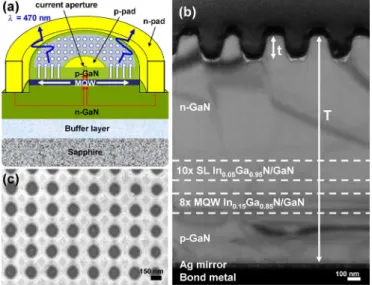
Fig. 1. Near-field and far-field sample structures. (a) Schematic diagram of the GaN-based blue LED structure with annular PhC region. (b) Cross-sectional TEM micrograph of a film-transferred GaN PhC LED structure with the etch depth t = 150 nm and GaN cavity thickness T = 1500 nm. (c) Top-view SEM image of PhCs on film-transferred LED with the lattice constant a = 350 nm and the diameter of air holes d = 200 nm fabricated with the holographic lithography.
manner. It is found that the emitted lights that are collinearly cou-pled to the reciprocal lattice are strongly TE polarized, while the noncollinearly coupled modes can posses both TE and TM po-larization. The complicated polarization pattern dependence of the PhC extracted light will have different reflection properties from the conventional light sources that need to be understood especially for illumination applications.
II. EXPERIMENTS
A. Sample Preparation
For near-field study, a special structure is used, as shown in Fig. 1(a). The GaN-based LED samples used in this study were grown by metal–organic chemical vapor deposition (MOCVD) on a c-axis sapphire (0 0 0 1) substrate. The LED structure (dominant wavelengthλ at 470 nm) was composed of a 1-µm-thick GaN bulk buffer layer on c-sapphire substrate, a 2-µm-thick bottom n-GaN current spreading layer, a 100-nm-2-µm-thick InGaN/GaN-active region consisting of multiple quantum wells (MQWs), and a 130-nm-thick top p-GaN current spreading layer. An annular region of square PhC lattice with an inner/outer diameter of 100/200 µm was patterned by holographic lithog-raphy. Two different periods of the lattice constant, 260 and
consists of a 150 nm In0.05Ga0.95N/GaN superlattice (SL) with
10 periods, a 120 nm In0.15Ga0.85N/GaN MQW active region
(dominant the wavelengthλ = 470 nm) with eight periods, a 20-nm-thick Mg-doped p-AlGaN electron blocking layer, a 300-nm-thick Mg-doped p-GaN contact layer. The detailed wafer processing of thin-film GaN LEDs associated PhC is the same as in [9], [10] using the laser lift-off technique to remove the growth substrate. The resulting structure is then thinned down by chemical–mechanical polishing (CMP) to obtain the GaN cavity thickness around 1500 nm. The PhC with a square lattice of circular holes was then defined by holography lithography. Holes were etched into the top n-GaN surface to a depth t = 150 nm. Fig. 1(b) shows the thin-film GaN PhC LED structure cross section of the transmission electron microscopy (TEM) image. The lattice constant a of PhC used for the far-field study is 290, 350, and 400 nm, and the hole diameter d is 200 nm. A scanning electron microscopy (SEM) image of the square lattice PhC structure is shown Fig. 1(c). Finally, a patterned Cr/Pt/Au (30/70/2000 nm) electrode was deposited on GaN as the n-type contact layer and Cr/Au (30/2000 nm) metal was deposited on Si substrate backside.
B. Experimental Setup
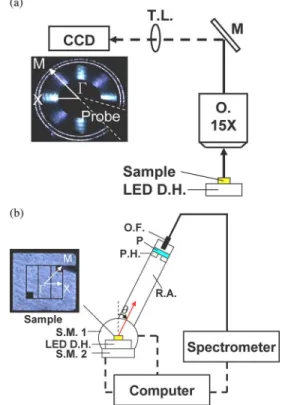
The schematics for the experimental setup are shown in Fig. 2(a) and (b) for near field and far field, respectively. An EL probe station system is utilized for the near-field ex-periment after fabrication, which included continuous wave (CW) current source (Keithley 238), a 15× microscope ob-jective with numerical aperture (NA) = 0.32. A 15× UV ob-jective with NA of 0.32 is used to collect the on-axis emission signal from the sample and formed a high-resolution image on a charge-coupled device (CCD) and recorded with a dig-ital camera. An example of the observed image is shown in the inset.
The angular-resolved measurement under electrical current injection was performed to study the far-field distribution us-ing a setup as shown in Fig. 2(b). A continuous current 20 mA was injected into the GaN film-transferred PhC LEDs packaged in transistor outline (TO) cans at room temperature. The light emission spectra were taken for every zenithal angle with 0.2◦ resolution from−90◦to +90◦. These spectra are then displayed on a wavelength versus angular plot with the color of the pixel
Fig. 2. (a) EL probe station and CCD imaging system setup, where D.H.: driver holder; M.: mirror; T.L.: tube lens; O.: objective. (b) Angular-resolved system setup, where S.M.: step motor; R.A.: rotating arm; P.H.: pinhole; P: polarizer; O.F.: optical fiber. Light emitted at the polar angle of θ, defined with respect to the direction normal to the sample surface, collected by optical fiber with a pinhole (diameter 1 mm) and a polarizer, which was placed at a distance of 15 cm from the sample. The sample was mounted on a rotating step motor 2 in order to find the correct in-plane direction from Γ−X to Γ−M .
representing the intensity of the spectra color-coded according to a scale bar. Spectra are collected along the Γ–X and Γ–M di-rections. The polarized spectra are then taken with the polarizer oriented in s- and p-directions.
III. RESULTS ANDDISCUSSION
Many different structures of PhC have been proposed and in-vestigated for various ways to tailor the beam properties for par-ticular applications. We investigated the square lattice because it is simple, retains the 2-D features, and is a model system for other slab structures. It is also the lattice structure that favors the polarized light emission [5]. The angular-resolved spectroscopic technique is a powerful method to investigate the quasiresonant modes that lie above the light lines to extract the waveguided lights. These quasiresonance modes are particularly important to assist the waveguided light to escape from LED chips [11]. A. Near Field
Using the annular sample structure shown in Fig. 1(a), the angular distribution of the near-field emission in the plane of the waveguide can be directly imaged. The details have been described before [3], only a brief discussion is given here.
The extraction of waveguided EL light into air can be de-scribed by the relation|k + G| < k0, where k is wave vector
Fig. 3. Ewald construction for a/λincreases above the cutoff and just start to couple with the shortest lattice vector GΓ X (a) in the Γ−X directions.
(b) Γ−M direction with the resultant wave vector falling outside the NA circle and will not be seen by the NA = 0.32 objective. (c) a/λincreases further as
nk0 just starts to leave the NA circle to disappear from the CCD image. The
solid circles are the NA cone and the dash circles are the waveguided mode cone.
of light and G is a reciprocal vector. For extraction into a cone with half angle θ, the relation is|k + G| < NA, where NA = sin θ and θ is the acceptance angle for the objective lens to collect the emitted light. For the present PhC structure, such a relation can be represented graphically with the Ewald con-struction projected on the waveguiding plane. An example of the Ewald construction is shown in Fig. 3. The two circles in each figure correspond to the waveguide mode circle (dashed blue) with radius k = 2πneff/λ at the outside, where neff is the
effective refractive index of the guided wave; and the NA circle with radius NA = 0.32koin the middle (red). When the in-plane
component of the resultant wave vector, after coupling to a re-ciprocal lattice vector, falls inside the NA circle, the diffracted light can escape into air and can be picked up with the objective lens.
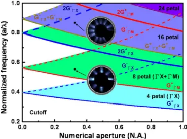
As shown in Fig. 3, as a/λ increases above the cutoff, the guided wave vector can couple with increasing number of recip-rocal points. The increased coupling possibilities are observed as the increased number of petals in the images.
For k > GΓX, the wave vector will start to couple with the
nearest neighbors lying at GΓX away and the resultant wave
vector falls inside the NA circle, as shown in Fig. 3(a). But for the Γ–M direction, the resultant wave vector fall outside the NA circle and will not be seen by the NA = 0.32 objective [Fig. 3(b)]. Therefore, a pattern with four petals pointing in the Γ–X direction is observed. As a/λ increases further, the resultant wave vector after coupling to GΓX may fall short of
the NA circle and will not be observed [Fig. 3(c)]. Thus, there is a range of a/λ within which the resultant wave vector can fall into the NA circle for a particular propagation direction. The boundary for this range in the Γ–X direction can be determined by the relation k =|GΓX − NA| to be a/λ = 1/(n+NA). When
a/λ increases further to the situation as shown Fig. 3(c), the resultant wave vector will leave the NA circle. In this case, k =|GΓX + NA| and a/λ = 1/(n−NA).
Fig. 4. Maps showing regions with different number of petals. The formula on the right of the figure is the boundary for regions. The insets showed the observed eightfold (a = 260 nm) and 16-fold (a = 410 nm) symmetry patterns. The regions of various petals are shown with different gray levels (color online). The directions of the petals are shown in the parenthesis. The “+” and “–” signs indicate the lower and upper boundary for the regions. The effective index used to generate the curves is n = 2.5.
For k > GΓM, the coupling to second nearest neighbor,
ly-ing at GΓM from the center, becomes possible and four more
petals appear corresponding to four equivalent Γ–M directions. For even larger lattice constants, coupling to the points lying at GΓX + GΓMaway is possible and the number of petals increases
to 16. The boundary separating the regions with different num-ber of petals depends and NA can be derived using the Ewald construction. The regions with different number of petals can be readily derived and is shown with different colors in Fig. 4 along with the examples of the observed CCD images.
The earlier discussion considers the simple case of single-mode propagation in the waveguide plane. Since the thickness of the epitaxial layer used for this study is 3 µm, the waveguid-ing is multimode. Every mode of these multimodes can couple with different reciprocal vectors to form their own boundaries for a given number of petals. When plotted on the map, these boundaries will appear as a ribbon of lines. Since, in reality, only a few modes out of the whole multimode ensemble are seen, for simplicity, only the case for one mode is shown in Fig. 4. B. Far Field
Far-field distribution of light sources is important for many applications. In PhC LED, the far-field distribution will be sig-nificantly modified by the PhC diffraction. The waveguided light traveling in the plane of wafer will be diffracted by the reciprocal wave vectors associated with the PhC. Due to the discrete na-ture of the waveguide modes, these diffracted light will exhibit anisotropy in the far-field pattern both in the zenith direction and the Azimuthal direction. In this study, the anisotropy in two high symmetry directions over a large range of a/λ was measured and discussed in the context of the band structure.
Fig. 5 shows the band structure for the TE modes in the present slab waveguide in the free photon limit with n = 2.5. Only
Fig. 5. Free photon band structure calculated with n = 2.5 for the TE modes. The thick lines indicate the collinear coupled bands. The thin lines indicated the noncollinear coupled bands. The boxes indicating the regions observed in this study with a = 290, 350, and 400 nm. The high symmetry points along the Γ-axis are labeled as Γ0through Γ4.
the TE modes are considered, since the present MQW struc-ture generates TE-polarized light propagating in the waveguide plane due to the valence band mixing of the QW light emission [12], [13]. Three different a values, 290, 350, and 400 nm, and the spectra spread of the present MQW sample, full-width at half-maximum (FWHM) = 50 nm, create a range of u = a/λ from 0.53 to 0.92 for experimental investigation, as enclosed in the boxes shown in Fig. 5. The air lines are shown as dashed lines. Above the air lines, the band structure exhibits an abun-dance of resonant states that will be involved in the PhC-assisted light extraction. Using the angular-resolved spectroscopic tech-nique, most of these states can be investigated efficiently. Fig. 6(a)–(c) shows the spectra taken along the Γ−X (left) and Γ−M (right) directions in unpolarized state for a = 290, 350, and 400 nm, respectively. These data can be transformed into dispersion curves to be compared with the calculated band structures shown in Fig. 5 that serves as a useful framework for the understanding of the experimental results. To examine the polarization of the spectra, a polarizer is used in front of the spectrometer with the polarization axis in the s- or p-orientation and the spectra retaken. It is found that certain lines are strongly polarized while the others have a mixed polarization. Due to the shallow etching of the present sample that results in a negligible narrow bandgap, the observed dispersion in this study was in good agreement with the calculated free photon band. The band structure shown in Fig. 5 essentially consists of bands emanat-ing from four symmetric points labeled as Γ1through Γ4on the
Γ-axis in Γ−X and Γ−M directions. These bands are formed by the collinear and noncollinear coupling with the recipro-cal vectors GΓX, GΓM, GΓX ΓX, and GΓX ΓM, respectively. The
thick lines marked the collinearly coupled bands, the rest of the bands are noncollinearly coupled bands. It will be shown that, for the present MQW samples, the collinearly coupled bands are singly degenerate and possess strong TE polarization. The noncollinearly coupled bands are doubly degenerate and have mixed polarization state.
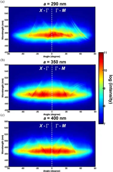
Fig. 6. Angular-resolved spectra without polarizer for lattice constant (a) a = 290 nm, (b) a = 350 nm, and (c) a = 400 nm, where Γ–X direc-tion points to the left and Γ–M direcdirec-tion points to the right.
To serve as an example for others, the case for a = 290 nm will be discussed in more detail. Fig. 6(a) shows the angular-resolved spectra taken from −90◦ to 90◦ with an accuracy of 0.2◦. It is found to be symmetrical around the vertical directions and consists of many sharp lines superimposed on the broad and diffuse Fabry–Perot background. The symmetry of the dis-tribution is a reflection of the present electrical current injection in which the recombination light radiates isotropically in the Azimuthal MQW plane. The narrow lines are the waveguide mode lines that are diffracted by the PhC s. The spectra are taken along the symmetric Γ−X and Γ−M directions after careful alignment. Only 4–6 modes are seen despite a total of 15 available modes for the waveguide based on the index pro-file shown in Fig. 1(b). The reasons may be the nonuniform coupling to the waveguide modes due to the uniform carrier dis-tribution, and different electric field overlap with the quantum wells among others.
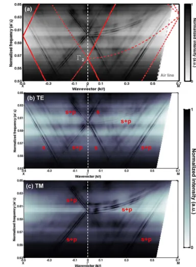
The a = 290 nm lattice corresponds to u = 0.53–0.65 cov-ering the Γ2 point. Fig. 8(a) shows the corresponding band
Fig. 7. Coupling diagram at (a) Γ1, (b) Γ2, (c) Γ3, and (d) Γ4 with
GΓ X, GΓ M, GΓ X Γ X, and GΓ X Γ M, respectively. The column A indicates the
wave vector coupling in the Γ–X direction and column B, the Γ–M direction. The red solid circles are the air cone. The thick arrows and thin arrows are the wave vectors.
data shown in Fig. 6(a) with k// = a sin θ/λ. It can be seen that the band structure in this range consists of two bands emaciat-ing from the Γ2 in the Γ−X direction and three in the Γ−M
direction. An examination of the polarized images shown in Fig. 8(b) and (c) reveals that the two bands in the Γ−X direc-tion possess mixed polarizadirec-tion. For the three bands in the Γ−M direction, the outer two bands of the three bands show strong TE polarization while the middle band with less dispersion has mixed state of the polarization. The reason for the mixed po-larization is due to the symmetric and antisymmetric coupling of the two degenerate states of this band as a result of the non-collinear coupling with the reciprocal wave vectors that results in a pseudo-TM mode [14], [15]. As shown in Fig. 7(b), Γ2,
for the modes traveling in the Γ−M directions, there are three bands resulted from coupling with the four equivalent GΓM
wave vectors pointing in four equivalent Γ−M directions. Two of the GΓMwave vectors are collinear with the Γ−M direction.
The other two are lying perpendicular to the Γ−M direction to provide noncollinear coupling with the modes propagating in the Γ−M direction. The noncollinear coupling forms the
Fig. 8. (a) Mode dispersions for a = 290 nm taken without the polarizer. The superimposed lines are the free photon band diagram with the solid lines corresponding to the singly degenerate band and dashed lines indicate doubly degenerated band. (b) and (c) Mode dispersion with the s- and p-polarization.
doubly degenerate band while the collinearly coupled band is singly degenerate. Fig. 8 (b) and (c) shows that the two strongly dispersed bands in the Γ−M directions are only observed in the s-polarized image indicating that the bands are TE-polarized. While the middle band is seen in both the s- and p-orientations indicating that they have a mixed polarization. For the Γ−X direction the modes can be noncollinearly coupled to the four equivalent wave vectors, GΓM’s and resulted in two doubly
de-generate bands (Fig. 7(b), Γ2, B). The two degenerate states in
each band are reduced to the symmetric and antisymmetric cou-pled states with the E field running perpendicular and parallel to the propagation direction, respectively. The symmetric cou-pled bands will have TE polarization, while the antisymmetric coupled bands will have TM polarization. In addition to these mode lines, two other families of lines, entering from below and pointing away from Γ-axis, appear in Fig. 8. They are part of the lines emanating from Γ1lying below. The bands emanating
from this point are actually formed in the same manner as that of Γ2, except that the coupling reciprocal wave vector is with the
GΓX’s (Fig. 7(a), Γ1, A and B). Collinear and noncollinear
cou-pling with GΓX’s result in the three bands emanating toward the
Fig. 9. (a) Mode dispersions for a = 400 nm taken without the polarizer. The superimposed lines are the free photon band diagram with the solid lines corresponding to the singly degenerate band and dashed lines indicate doubly degenerated band. (b) and (c) Mode dispersion with the s- and p-polarizations.
that for the Γ2 point. The noncollinearly coupled mode lines
entered the image from the bottom in the Γ−M sector of Fig. 8 and exhibit a mixed polarization while the collinearly coupled mode lines appear in the Γ−X sector have the TE polarization. The experimentally observed bands appear to be shifted away from the calculated lines. The bands are also appeared to be shifted from sample to sample when displayed in the present scale. There are several factors causing the shifts. Due to the shallow PhC, the field of low-order modes has poor overlap with the PhC and will not been extracted, hence the low-order modes with effective indexes close to that used for the calculated lines are missing. In addition, the thickness of the sample also varies by 100–200 nm due to the sample tilting during lapping and thinning to cause an uncertainty in the thickness of the waveguide. Such a variation will cause a corresponding shift in the effective indexes for the waveguiding modes, which in turn cause the mismatch of the bands from sample to sample. Taking these factors into account the agreement between the experiment and calculation are reasonably good.
For the Γ3 point, the band structure resembles that at Γ1, but
the wave vectors involved here have the length of two GΓX.
Fig. 10. (a) Mode dispersions for a = 350 nm taken without the polarizer. The superimposed lines are the free photon band diagram with the solid lines corresponding to the singly degenerate band and dashed lines indicate doubly degenerated band. (b) and (c) Mode dispersion with the s- and p-polarizations.
The a/λ is also twice that at Γ1, thus the bands appears to be
identical to those at Γ1 except that they are shifted up to the
Γ3 point, as shown in Fig. 9. The polarization for each of the
bands is also the same as that of Γ1. In addition to the bands
emanating from the Γ3 point, there are some bands that come
from the Γ4point lying above shown in Fig. 10. The Γ4point is
different from Γ1, Γ2, and Γ3. There are four bands, instead of
three and two, at Γ2and Γ3, respectively, emanating from this
point for both directions. An analysis indicates that these bands actually result from the eight equivalent GΓX ΓM’s for the Γ point
(Fig. 7(d), Γ4, A and B). For the Γ−X directions these eight
vectors arranged in four symmetric pairs that can noncollinearly couple to the k vectors to form four double degenerate bands. For the Γ−M directions, there are also four such pairs that can couple to the k vectors and resulted in four bands that are emanating from the Γ4 point. These two groups of four bands
are all doubly degenerate and posses mixed polarization. The two lowest bands from the two groups are seen in Fig. 9(a) (one of them barely visible). The two bands entering the image field from above and pointing away from the Γ-axis in either
direction appear in both polarizations, as shown in Fig. 9(b) and (c).
Fig. 10 depicts the band structure that appeared in the a = 350 nm lattice. It mainly consists of bands that are emanating from Γ2 point lying below and the Γ3 and Γ4 points lying
above. The polarizations of these modes are in agreement with the discussion shown earlier. However, it should be noted that at the crossover point away from the Γ-axis, the anticrossing formed by the two bands is not observed due to the present shallow etching [12].
IV. CONCLUSION
Experimental investigation of the near-field and far-field dis-tribution has been conducted on GaN LEDs with square PhC lattice. The near-field distribution, studied in the Azimuthal di-rection with a specially designed waveguide structure, shows a symmetric pattern with varying number of petals in the plane of the waveguide. The regions corresponding to varying number of petals are determined for increasing lattice constant. The far field was studied with GaN-based film-transferred PhC LEDs with the GaN thickness about 1500 nm. Angular-resolved measure-ments under electrical injection revealed guided modes extrac-tion behavior based on the Bragg’s diffracextrac-tion with the lattice. Due to the shallow etching of the present case, the dispersion curve of the mode lines observed in the angular-resolved spectra closely resemble the band structures of the free photon band with the index corresponding to the average index for the slab waveg-uides. Polarization of the emitted lines has also been studied and a dependence of the polarization on the collinear or noncollinear coupling with the reciprocal wave vectors was observed. Good agreement with the 2-D free photon approximation was ob-tained. The present results indicate that the PhC-enhanced LED will have complicated polarization distribution that will have implication for the use of these LEDs as the light sources for display and lighting.
ACKNOWLEDGMENT
The authors gratefully acknowledge Dr. S. C. Wang from National Chiao Tung University (NCTU), Taiwan, for technical support.
REFERENCES
[1] M. R. Krames, O. B. Shchekin, R. Mueller-Mach, G. O. Mueller, L. Zhou, G. Harbers, and M. G. Craford, “Status and future of high-power light-emitting diodes for solid-state lighting,” J. Display Technol., vol. 3, pp. 160–175, 2007.
[2] C. F. Lai, H. C. Kuo, C. H. Chao, H. T. Hsueh, J.-F. T. Wang, W. Y. Yeh, and J. Y. Chi, “Anisotropy of light extraction from two-dimensional photonic crystal light-emitting diodes,” Appl. Phys. Lett., vol. 91, pp. 123117-1– 123117-3, 2007.
[3] C. F. Lai, J. Y. Chi, H. C. Kuo, C. H. Chao, H. T. Hsueh, J.-F. T. Wang, and W. Y. Yeh, “Anisotropy of light extraction from two-dimensional photonic crystals,” Opt. Exp., vol. 16, pp. 7285–7294, 2008.
[4] J. J. Wierer, M. R. Krames, J. E. Epler, N. F. Gardner, and M. G. Craford, “InGaN/GaN quantum-well heterostructure light-emitting diodes employ-ing photonic crystal structures,” Appl. Phys. Lett., vol. 84, pp. 3885–3887, 2004.
[5] C. F. Lai, J. Y. Chi, H. H. Yen, H. C. Kuo, C. H. Chao, H. T. Hsueh, J.-F. T. Wang, C. Y. Huang, and W. Y. Yeh, “Polarized light emission from photonic crystal light-emitting diodes,” Appl. Phys. Lett., vol. 92, pp. 243118-1–243118-3, 2008.
[6] A. David, T. Fujii, B. Moran, S. Nakamura, S. P. DenBaars, C. Weisbuch, and H. Benisty, “Photonic crystal laser lift-off GaN light-emitting diodes,”
Appl. Phys. Lett., vol. 88, pp. 133514-1–133514-3, 2006.
[7] K. Bergenek, Ch. Wiesmann, R. Wirth, L. O’Faolain, N. Linder, K. Streubel, and T. F. Krauss, “Enhanced light extraction efficiency from AlGaInP thin-film light-emitting diodes with photonic crystals,” Appl.
Phys. Lett., vol. 93, pp. 041105-1–041105-3, 2008.
[8] M. Yokoyama and S. Noda, “Polarization mode control of two-dimensional photonic crystal laser having a square lattice structure,” IEEE
J. Quantum Electron., vol. 39, no. 9, pp. 1074–1080, Sep. 2003.
[9] C. F. Lai, J. Y. Chi, H. H. Yen, C. E. Lee, H. C. Kuo, C. H. Chao, H. T. Hsueh, C. Y. Huang, J.-F. T. Wang, W. Y. Yeh, T. C. Lu, and S. C. Wang, “Extraction enhancement and collimation from a thin-film InGaN/GaN photonic crystal light-emitting diodes,” in Proc. ’08 SSDM
E-10–2, pp. 988–989.
[10] C. E. Lee, C. F. Lai, Y. C. Lee, H. C. Kuo, T. C. Lu, and S. C. Wang, “Nitride-based thin-film light-emitting diodes with photonic quasi-crystal surface,” IEEE Photon. Technol. Lett., vol. 21, pp. 331–333, 2009. [11] F. S. Diana, A. David, I. Meinel, R. Sharma, C. Weisbuch, S. Nakamura,
and P. M. Petroff, “Photonic crystal-assisted light extraction from a col-loidal quantum dot/GaN hybrid structure,” Nano Lett., vol. 6, pp. 1116– 1120, 2006.
[12] A. David, C. Meier, R. Sharma, F. S. Diana, S. P. DenBaars, E. Hu, S. Nakamura, and C. Weisbuch, “Photonic bands in two-dimensionally patterned multimode GaN waveguides for light extraction,” Appl. Phys.
Lett., vol. 87, pp. 101107-1–101107-3, 2005.
[13] M. F. Schubert, S. Chhajed, J. K. Kim, E. F. Schubert, and J. Cho, “Po-larization of light emission by 460 nm GaInN/GaN light-emitting diodes grown on (0001) oriented sapphire substrates,” Appl. Phys. Lett., vol. 91, pp. 051117-1–051117-3, 2007.
[14] T. Ochiai and K. Sakoda, “Nearly free-photon approximation for two-dimensional photonic crystal slabs,” Phys. Rev. B, vol. 64, pp. 045108-1– 045108-11, 2001.
[15] V. Pacradouni, W. J. Mandeville, A. R. Cowan, P. Paddon, and J. F. Yong, “Photonic band structure of dielectric membranes periodically textured in two dimensions,” Phys. Rev. B, vol. 62, pp. 4204–4207, 2000.
Chun-Feng Lai received the M.S. degree in the
electro-mechanical engineering from the National Sun Yat-Sen University, Kaohsiung, Taiwan, in 2005. He is currently working toward the Ph.D. degree in the Department of Photonics and Institute of Electro-Optical Engineering, National Chiao Tung University (NCTU), Hsinchu, Taiwan.
His current research interests include high ef-ficiency GaN-based LED and GaN film-transferred LED via photonic crystals.
Jim-Yong Chi (SM’97) received the B.S. degree
in physics from the National Tsinghua University, Hsinchu, Taiwan, in 1971, and the Ph.D. degree in material science from the Massachusetts Institute of Technology, Cambridge, in 1979.
He joined the Industrial Research and Technology Institute, Taiwan, in 1999. He joined the National Dong Hwa University, Hualien, Taiwan, as a Profes-sor and the Director of the Institute of Optoelectronic Engineering in 2008. He was a Member of Technical Staff in Lucent Technologies, Bell Laboratories, GTE Laboratories, Polaroid Corporations, and AMP M/A-COM. He has authored or coauthored more than 200 technical papers and conference papers and has given many invited talks at conferences and institutions.
Dr. Chi won many awards including the 2004 Distinguished Engineers Award by the Association of Chinese Engineers, Taiwan.
materials, and solar cell. He has authored or coauthored 140 internal journal papers, and 6 granted and 10 pending patents.
Prof. Kuo is the IEEE Senior Member and Associate Editor of IEEE/OSA JOURNAL OFLIGHTWAVETECHNOLOGYand IEEE JOURNAL OFSELECTED TOP-ICS INQUANTUMELECTRONICS(JSTQE)—special issue on Solid-State Lighting. He received Ta-You Wu Young Scholar Award from the National Science Coun-cil and Young Photonics researcher award in 2007.
Hsi-Hsuan Yen received the M.S. degree from the
Department of Physics, National Central University, Taoyuan, Taiwan, in 2001. He is currently work-ing toward the Ph.D. degree in Department of Pho-tonics and Institute of Electro-Optical Engineering, National Chiao Tung University (NCTU), Hsinchu, Taiwan.
His current research interests include high effi-ciency based LED and alternating current GaN-based LED devices.
Chia-En Lee received the B.S. and M.S. degrees in
the electrical engineering from the National Chung Hsing University, Taichung, Taiwan, in 2002 and 2004, respectively. He is currently working toward the Ph.D. degree from the Department of Photon-ics and Institute of Electro-Optical Engineering, Na-tional Chiao Tung University (NCTU), Hsinchu, Taiwan.
His current research interests include the nitride-based LEDs.
Wen-Yung Yeh received the Ph.D. degree in
materi-als science and engineering from National Tsing Hua University, Hsinchu, Taiwan, in 2001.
He is currently the Deputy Director of the Opto-Electronic Device and System Application Division, Electronics and Opto-Electronics Research Laborato-ries (EOL), Industrial Technology Research Institute (ITRI), Hsinchu, Taiwan, where he leads the AC LED research team. His current research interests include photonic crystal LED, AC LED, and GaN solar cell. Dr. Yeh received the R&D 100 Award in 2008.
Tien-Chang Lu received the B.S. degree in
elec-trical engineering from National Taiwan University, Taipei, Taiwan, in 1995, the M.S. degree in elec-trical engineering from the University of Southern California, Los Angeles, in 1998, and the Ph.D. de-gree in electrical engineering and computer science from National Chiao Tung University, Hsinchu, Tai-wan, in 2004.
Since August 2005, he has been with the Depart-ment of Photonics, National Chiao Tung University (NCTU), Hsinchu, Taiwan, as a Faculty Member.