An Integrated 60-GHz Front-end Receiver with a
Frequency Tripler Using 0.13-µm CMOS Technology
Po-Hung Chen, Min-Chiao Chen, and Chung-Yu Wu
Nanoelectronics and Giga-scale Systems Laboratory, Institute of Electronics, National Chiao Tung University,Hsinchu City, Taiwan
Abstract—In this paper, a 60-GHz CMOS direct-conversion
receiver integrated with a frequency tripler is proposed. The proposed receiver consists of a low-noise amplifier (LNA), a down-conversion mixer, output buffers, and a frequency tripler. This chip is designed using 0.13-um CMOS technology. By using a frequency tripler, the operating frequency of the PLL can be reduced from 60 GHz to 20 GHz. This makes the implementation of the PLL much easier. According to the simulation results, the receiver has a noise figure (NF) of 7.6 dB, a power gain of 29.2 dB. It consumes 14.2 mW from a 1.2-V power supply.
I. INTRODUCTION
Recently, a 7-GHz band covering the range between 57 and 64 GHz has been released for unlicensed use in high-speed and short-range communication systems. It has great potential in the application of high speed WLAN and point-to-point links, and offers a possible data rate of gigabits per second. Existing millimeter wave receivers which use SiGe or HEMT have the potential to implement wireless components for 60-GHz applications due to the latter’s high unit current gain frequency (fT) [1]-[2]. However, as the fT reaches 80 GHz in 0.13-um bulk CMOS technology, the advanced bulk CMOS technology becomes the potential choice for the implementation the high speed wireless components. Bulk CMOS technology also has the advantages of low cost and a high level of integration.
Several 60-GHz CMOS receivers have been reported in [3]-[5]. In [3], a direct-conversion receiver with a two-stage LNA and Gilbert cell based mixer is presented. However, this type of architecture requires a 60-GHz PLL to generate the LO signal, but such a PLL is difficult to implement and has poor performance. In [4], a heterodyne receiver integrated with a LO signal generator and divider is implemented using 90-nm CMOS technology. In this architecture, a high speed frequency divider is required, and leads to a large power consumption. In [5], a receiver integrated with a frequency doubler is presented. However, the doubler can not provide the differential output signal associated with a mixer and such a circuit still consumes a large amount of power.
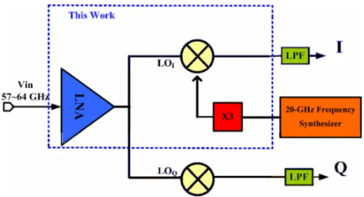
Figure 1. The proposed receiver architecture with frequency tripler.
In this paper, a CMOS direct-conversion receiver integrated with a frequency tripler is proposed and simulated using 0.13-um CMOS technology. Direct-conversion architecture provides the advantages of high integrity and low cost. Moreover, the architecture is simple. A frequency tripler requires a 20-GHz PLL only and is much easier to design [6]-[7]. A relatively low frequency PLL can provide a better performance in comparison with PLLs cited elsewhere [3]-[5]. From the simulation results, the overall noise figure (NF) is 7.6~8.2 dB, the power gain is 29.2dB with a 3dB-bandwidth form 55.5 to 65 GHz which covers the whole unlicensed band of around 60 GHz; and the input-referred 1-dB compression point is -25.8 1-dBm. It drains 11.8 mA from 1.2-V power supply.
II. RECEIVER ARCHITECTURE AND CIRCUIT
IMPLEMENTATION
Fig.1 shows the block diagram of the proposed receiver. It consists of a LNA, a down-conversion mixer, output buffers and a frequency tripler. First of all, the RF input signal is amplified by the LNA which has a reasonable gain to enhance the signal to noise ratio (SNR). The down-conversion mixer following the LNA provides extra gain and down converts the RF signal to an IF band by mixing with the LO signals. To obtain the desired LO signal, the 20GHz differential input signal is put through a frequency tripler to produce 60 GHz. Because of the poor properties of the active
This work was supported by the National Science Council (NSC) of Taiwan, under Grant NSC-95-2221-E-009-292-
devices at the frequency near fT, the circuit would be much easier to design if VCO at a lower frequency are used. More specifically, using a low frequency PLL connected to a frequency tripler to generate LO signals can achieve a better phase noise performance and the power consumption of the frequency pre-scalar can be greatly reduced due to a lower operating frequency. For the purpose of measurement, an output buffer is exploited in this study for the 50-ohm load. The building blocks in Fig.1 are described in the following subsections.
A. Low Noise Amplifier Design
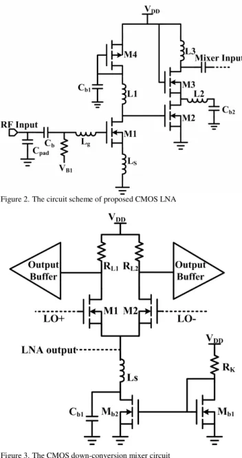
A two-stage single-ended LNA is implemented as shown in Fig.2. The first stage dominates the input matching ability and overall noise performance because the gain of the first stage can suppress the noise contribution from the subsequent stages. In order to improve gain and noise performances, a common-source with source degeneration topology is applied. By selecting the appropriate values of the degeneration inductor LS and the gate inductor Lg, noise and input impedance matching at the desired frequency can be achieved.
The second stage is implemented by using a cascode structure as the other gain stage and this provides the output current to the next stage. The conventional cascode structure provides the advantages of a low noise figure, a high gain and a high reverse isolation at a frequency much lower than fT; as a result, the performances of gain and noise are degraded. Therefore, the inductive peaking technique is applied in this study to resonate with the parasitic capacitance at the drain of M2 and to improve the performance of this stage. This scheme not only provides better noise and gain performances but it also improves the degree of isolation.
So far, most of the previously reported multi-stage cascaded LNAs bias each stage separately by using blocking capacitors to reduce power consumption [5]. However, the non-ideal effect and parasitic capacitance of the passive components would also contribute some noise referring to the input and increase the overall noise figure. Moreover, the dc blocking capacitances also cause a signal decrease due to the parasitic capacitance of the input MOSFET and therefore the small signal gain decreases. To solve this problem, the dc voltage of the second stage is appropriately designed by using a PMOS load M4 as shown in Figure-2. The capacitance Cb1 is a bypass capacitance which provides an ac ground path at the drain of M4.
B. Down-conversion Mixer.
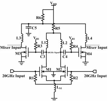
To increase the mixer linearity by alleviating the output signal headroom, the current mode interface between the LNA and mixer presented in [8] is used in this study. The proposed mixer architecture is shown in Fig.3. The trans-conductance stage which converts the voltage signal to current signal in a conventional Gilbert cell mixer can be removed.
Figure 2.The circuit scheme of proposed CMOS LNA
Figure 3.The CMOS down-conversion mixer circuit
The RF current is coupled from the output of the LNA through the dc blocking capacitance and fed into the source of the differential pair, M1,2 to mix with the LO signals.
A current mirror implemented by Mb1,b2 generates the desired dc current to the differential pair. To avoid the noise contribution from the current source, a large bypass capacitance Cb1 is applied to filter out the flicker noise. The inductor LS is used to resonate with parasitic capacitance at the source terminal of M1,2 at the desired frequency. This inductor could reduce the signal loss caused by the parasitic capacitance The capacitance Cp1,p2 and RL1,L2 function as a low pass filter to extract the undesired signal. Due to the low-pass characteristics of the filter, the LO to IF isolation can be markedly improved. To reduce the IF signal loss resulting from the low pass filter at the output of the mixer, the pole of the filter needs to be selected appropriately. For
measurement considerations, MOS M3 and M4 are used as unit-gain buffers to drive the 50-ohm measurement system.
In comparison with a conventional mixer, the proposed mixer has the following advantages. First, the noise figure is better due to the absence of the noise resulting from the input stage in a conventional mixer. Second, the supply current only needs to provide the mixing stage M1,2 in this case and the dc current can be reduced to improve the noise performance even more. Finally, an improvement in linearity is expected due to the enhancement of headroom and input stage that dominates the linearity of a conventional structure.
An increase in RL1,L2 results in an increase in conversion gain but a decrease in the DC voltage at the output nodes. In short, there is a trade-off between conversion gain and linearity.
C. Frequency Tripler
Fig.4 shows the proposed frequency tripler circuit. As the fundamental signal is applied to the gate terminals of M1 and M2, the third harmonic signal can be amplified by using the inductors L1 and L2 to resonant with the parasitic capacitance at the third harmonic frequency of the input signal. To improve the performances of the frequency tripler, the source inductor LS is applied here. This inductor is used to enhance the even order harmonics at the source terminal of M1,2 in order to mix with the input signal. Thus, the third harmonic signals at the output nodes can be enhanced further. When even-order harmonics are involved, the LS can be seen as a source degeneration inductance and a cause of reduced even order signal gain. Because the even harmonic signals at the output nodes are a common-mode signal, the common load resistance R5 can be designed to eliminate the undesired even harmonic signals.
Figure 4.The circuit scheme of proposed CMOS frequency tripler
The M3 and M4 perform as CS amplifiers and the load inductors L3 and L4 are resonated at the third harmonic frequency of the fundamental. By using additional gain stage, not only can the desired signal be enhanced further but also the other undesired harmonics can also be suppressed.
III. SIMULATION RESULTS OF RECEIVER
The 60-GHz receiver front-end is designed and simulated using 0.13-um 1P8M Cu CMOS technology with ultra thick 3.3-um metal. The chip is under fabrication and chip layout is depicted in Fig.5, with a total die area of only 0.63 mm2 including all test pads and dummy metal. In order to avoid any coupling effects, the space between the T-lines are more than three-times that of the metal width. All of the T-lines characteristics are simulated using an EM simulator, Ansoft HFSS. The circuit simulation uses Agilent Advanced Design System (ADS) software. The circuit is biased at a 1.2-V supply voltage with current consumption of 4.7, 0.6, and 6.5 mA for the LNA, mixer, and frequency tripler respectively. The total dc power consumption is only 14.2 mW.
However, without inter-stage matching between the mixer and the frequency tripler, maximum voltage swing can be achieved. Therefore, the dc gate bias of the mixer LO port is designed using a dc drop across the resistance of the previous stage. The simulation results are expressed when the IF signal is 100MHz and Fig.6,Fig.7 shows the simulation results of the proposed direct conversion receiver. The maximum conversion gain for the receiver is 29.2 dB with 3dB bandwidth ranging from 55.5 to 65 GHz. The simulated minimum NF various from 7.6 to 8.2 dB and P1dB is -23.4 to -25.8 dBm over the 7-GHz unlicensed band around 60 GHz. The simulated performance parameters of the proposed direct-conversion receiver are summarized in Table I where comparisons with recently published 60GHz receivers are also included. As can be seen, the proposed receiver could achieve a lower noise figure performance and also has a reasonable conversion gain and linearity performance with lower power consumption.
IV. CONCLUSION
Employing 0.13-um CMOS technology, a 60-GHz CMOS direct-conversion receiver with a frequency tripler using a 1.2 V supply is simulated in this study and under fabrication. The receiver consists of a two-stage LNA, a single-balanced active mixer, a frequency tripler, and output buffers. By using the frequency tripler, only 20-GHz PLL is required to generate the 60GHz LO signal to down convert the RF signal to a base-band frequency from which a better performance is expected. At the desired frequency band between 57 to 64 GHz and for a 100 MHz IF output, the proposed receiver provides a conversion gain greater than 27.6 dB and a noise figure less than 8.2 dB with a maximum conversion gain of 29.2 dB and minimum noise figure of 7.6 dB at 61 GHz RF frequency. Furthermore, the circuit could provide the input P1dB better than -25.8 dBm and a total power consumption including the frequency tripler is 14.2 mW.
Figure 5.The circuit scheme of proposed CMOS frequency tripler
Figure 6.Simulation results of conversion gain and noise figure
Figure 7.Simulation results of lieanrity, P1dB
TABLE I. PERFORMANCE SUMMARY AND COMPARISON Reference [3] [5] This work Frequency (GHz) 57.5~64 57~63 55.5-65 LNA Gain (dB) 13.2 12 13.7 LNA NF (dB) 4.6~5.4 8.8 4.3~4.6 LNA Power (mW) 4.8 43.2 5.6 Mixer Gain (dB) 12 -2 15.5 Mixer NF (dB) 18.5~19.5 13.8 8.5~9.5 Mixer Power (dB) 1.1 2.4 0.7 Receiver Gain(dB) 28* 11.8 29.2 Receiver NF(dB) 12.5 10.4 7.6 P1dBin(dBm) -22.5 -15.8 -25.8
IF Amplifier Yes Yes No Technology 0.13-um CMOS 0.13-um CMOS 0.13-um CMOS *Including IF amplifier ACKNOWLEDGMENTS
The authors would like to thank the Chip Implementation Center (CIC) and the National Science Council, Taiwan for the fabrication of the chip. We also appreciate the EM simulator and advice provided by Ansoft. The Chip is being fabricated by Taiwan Semiconductor Manufacturing Company (TSMC).
REFERENCES
[1] B. A. Floyed, S. K. Reynolds, U. R. Preiffer, T. Zwick, T. Beukema and B. Gaucher, “ SiGe Bipolar Transceiver Circuits Operating at 60GHz” IEEE J. Solid-State Circuits, vol. 40,no. 1, Jan. 2005. [2] S. E. Gunnarsson, C. Karnfelt, H. Zirath, R. Kozhuharov, D.
Kuylenstierna, C. Fager and A. Alping,”Single-Chip 60 GHz Transmitter and Receiver MMICs in a GaAs mHEMT Technology” in IEEE MTT-S Int. Microwave Symp., Dig., Jun. 2006, pp. 801-804. [3] B. Razavi, “A 60-GHz CMOS Receiver Front-End,” IEEE J.
Solid-State Circuits, vol. 41, pp. 17-22, Jan. 2006.
[4] B. Razavi, “A mm-Wave CMOS Heterodyne Receiver with on-Chip LO and Divider,” IEEE J. Solid-State Circuits, vol. 41, pp. 17-22, Jan. 2006.
[5] S. Emami, C. H. Doan, A. M. Niknejad and R. W. Brodersen, “A Highly integrated 60GHz CMOS Front-End Receiver” ISSCC Dig.
Tech. Papaers, pp. 190-191, Feb. 2007.
[6] A. Boudiaf, D. Bachelet, and C. Rumelhard, “A high-efficiency and low-phase-noise 38-GHz pHEMT MMIC tripler,” IEEE Trans.
Microwave Theory and Tech., vol. 48, no. 12, pp. 2546–2553, Dec. 2000.
[7] Y. Campos-Roca, L. Verweyen, M. Fernández-Barciela, E. Sánchez, M. C. Currás-Francos, W. Bronner, A. Hülsmann, and M. Schlechtweg, “An optimized 25.5–76.5 GHz pHEMT-based coplanar frequency tripler,” IEEE Microwave and Guided Wave Letters, vol. 10, no. 6, pp. 242–244, Jun. 2000.
[8] H. Sjoland et al., “A merged CMOS LNA and mixer for a WCDMA receiver,” IEEE J. Solid-State Circuits, vol. 38, no. 6, pp. 1045–1050, Jun. 2003.