Formation and nonvolatile memory characteristics of multilayer nickel-silicide NCs
embedded in nitride layer
Wei-Ren Chen, Ting-Chang Chang, Jui-Lung Yeh, S. M. Sze, and Chun-Yen Chang
Citation: Journal of Applied Physics 104, 094303 (2008); doi: 10.1063/1.3006126
View online: http://dx.doi.org/10.1063/1.3006126
View Table of Contents: http://scitation.aip.org/content/aip/journal/jap/104/9?ver=pdfcov Published by the AIP Publishing
Articles you may be interested in
Effect of annealing treatment on the electrical characteristics of Pt/Cr-embedded ZnO/Pt resistance random access memory devices
J. Vac. Sci. Technol. A 32, 02B119 (2014); 10.1116/1.4865551
Switching mechanism transition induced by annealing treatment in nonvolatile Cu/ZnO/Cu/ZnO/Pt resistive memory: From carrier trapping/detrapping to electrochemical metallization
J. Appl. Phys. 106, 123705 (2009); 10.1063/1.3273329
Formation of cobalt-silicide nanocrystals in Ge-doped dielectric layer for the application on nonvolatile memory Appl. Phys. Lett. 92, 152115 (2008); 10.1063/1.2908916
Reliability characteristics of NiSi nanocrystals embedded in oxide and nitride layers for nonvolatile memory application
Appl. Phys. Lett. 92, 152114 (2008); 10.1063/1.2905812
Nonvolatile memory characteristics influenced by the different crystallization of Ni–Si and Ni–N nanocrystals Appl. Phys. Lett. 92, 062112 (2008); 10.1063/1.2841049
Formation and nonvolatile memory characteristics of multilayer
nickel-silicide NCs embedded in nitride layer
Wei-Ren Chen,1Ting-Chang Chang,2,a兲 Jui-Lung Yeh,3S. M. Sze,3and Chun-Yen Chang3
1
Institute of Electronics, National Chiao Tung University, Taiwan, Hsin-Chu 300, Taiwan
2
Department of Physics and Institute of Electro-Optical Engineering, and Center for Nanoscience and Nanotechnology, National Sun Yat-Sen University, Kaohsiung 804, Taiwan
3
Institute of Electronics, National Chiao Tung University, Taiwan, Hsin-Chu 300, Taiwan
共Received 20 June 2008; accepted 9 September 2008; published online 5 November 2008兲 The authors provided the formation and memory effects of nonvolatile multilayer nickel-silicide nanocrystal memory in this study. This proposed structure can efficiently improve the drawbacks of current floating gate and single-layer nanocrystal memories for the next-generation nonvolatile memory application. The charge trapping layer of multilayer structure was deposited by sputtering a commixed target共Ni0.3Si0.7兲 in the argon and nitrogen ambiance, and then used a low temperature
rapid thermal annealing to form uniform nanocrystals. Transmission electron microscope images clearly show the multilayer and single-layer nanocrystal structures embedded in SiNx. X-ray photoelectron spectroscopy and x-ray diffraction also present the chemical states and crystallization of nanocrystals under different annealing temperature treatments. The capacitor with different memory structures was also studied and exhibited hysteresis characteristics after electrical operation. In addition, the multilayer nanocrystals revealed better charge storage ability and reliability than the single-layer nanocrystals. © 2008 American Institute of Physics. 关DOI:10.1063/1.3006126兴
I. INTRODUCTION
Nonvolatile nanocarbon 共NC兲 memories and poly-silicon-oxide-nitride-oxide-silicon 共SONOS兲-type memories have recently been promising candidates to take the place of the conventional floating gate nonvolatile memory because the discrete quantum wells and traps as the charge storage media have effectively improved data retention for the scal-ing down devices.1–3Although the scaling down tunnel oxide 共⬍4 nm兲 is defect-free and of high quality, it is still difficult to prevent the storage charges to leak into substrate under retention test. Because of the quantum effect factor, the wave function of stored electrons can appear in the silicon sub-strate resulting in larger tunneling probability to increase the charge loss for retention state.4,5 In the pervious studies, the high-k materials can be used to increase the physical thick-ness of tunnel oxide layer and achieve the same efficiency for scaling down process, such as Si3N4, HfO2, and Al2O3.4,6 Moreover, Ng et al.7proposed a densely stacked silicon NC layer to keep the better retention time because the charges stored in the NCs near the blocking oxide have low tunnel probability to leak into substrate. However, there are very few researches to investigate the formation and nonvolatile memory effect of multilayer metal NCs.
In our work, the formation and charge storage effect of nonvolatile multilayer nickel-silicide 共NiSi兲 NC memory 共NMLNCM兲 were revealed. The NCs were formed by the Ni–Si–N thin film and this proposed that memory structure was combined with the benefits of SONOS-type and multilayer NCs. Hence, we used the NMLNCM structure to
compare with single-layer nickel-silicide NCs for the electri-cal characteristics of capacitance-voltage 共C-V兲, retention, and endurance test in this study.
II. FABRICATION FLOW AND MATERIAL ANALYSES OF NCS
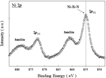
This memory cell structure was fabricated on a 4 in. p-type silicon 共100兲 wafer. After a standard RCA process, which removed native oxide and microparticles, a 3-nm-thick tunnel oxide was thermally grown by a dry oxidation process in an atmospheric pressure chemical vapor deposi-tion furnace. Subsequently, a 10-nm-thick nitrogen incorpo-rated Ni0.3Si0.7layer that served as the charge trapping layer was deposited by reactive sputtering of Ni0.3Si0.7commixed target in the Ar 关24 SCCM 共SCCM denotes standard cubic centimeter per minute at STP兲兴 and N2共10 SCCM兲 environ-ment at room temperature. The dc sputtering power and pres-sure were set to 80 W and 7.6 mtorr. Here, the ratio of com-mixed target共Ni:Si兲 was decided by the volumes of NCs and surrounding dielectric. We first analyzed the composition of the charge trapping layer by x-ray photoelectron spectros-copy 共XPS兲 system. Figure 1 shows the Ni 2p core-level photoemission spectra of the charge trapping layer which consist of two main peaks, 2p3/2 共⬃855 eV兲 and 2p1/2
共⬃873 eV兲, with two small satellite peaks by XPS system. According to the values of other literatures, Ni 2p3/2binding
energies are at 852.3 and 853.4 eV for metallic nickel 共Ni– Ni兲 and Ni-silicide 共Ni–Si兲, respectively.8
However, it can not found that the above-mentioned peak signals are ob-served at the Ni 2p3/2 peak by our XPS result. Due to the
strong electronegativity of nitrogen atom, the binding energy of Ni–Si bond would shift toward higher binding energy if
a兲Electronic mail: [email protected].
0021-8979/2008/104共9兲/094303/6/$23.00 104, 094303-1 © 2008 American Institute of Physics
the nitrogen atoms were bound with the Ni–Si compound. At this point, it was reasonably assumed that the charge trapping layer 共as deposited thin film兲 could be assigned to the Ni– Si–N ternary bond. Hence, we could obtain a Ni–Si–N thin layer that serves as the charge trapping layer by sputtering a Ni0.3Si0.7target in the Ar/N2 environment in our work.
Next, a rapid thermal annealing共RTA兲 process was per-formed in N2 ambient and the annealing condition was
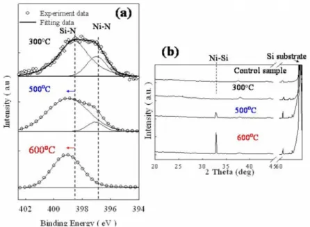
600 ° C for 100 s. After the annealing step, the NCs would self-assemble in the dielectric layer, and the single-layer NC memory structure was formed by capping a 30-nm-thick SiO2as the blocking oxide. The cross-sectional transmission electron microscope共TEM兲 and fabrication flow of NCs em-bedded in the nitride layer are shown in Fig. 2. Here, we further analyzed the chemical states of NCs to find that the peak signal of Si–N bond was shifted toward higher binding energy, and the peak signal of Ni–N was decayed gradually to disappear after the RTA process at 600 ° C for 100 s by the N 1s results of XPS, as shown in Fig.3共a兲. Besides, we also found that the peak of Ni–Si obviously appeared at 32.8° by x-ray diffraction共XRD兲 analysis after the annealing tempera-ture treatment of 500 ° C, as shown in Fig. 3共b兲. Therefore, we considered this as an internal competition characteristic of Ni–Si–N thin film due to the different Gibbs free energy
of Ni–Si 共−318 kJ mol−1兲, Ni–N 共−70–85 kJ mol−1兲, and
Si–N共−470 kJ mol−1兲 to simply form the uniform NiSi NCs
embedded in the nitride layer9
Moreover, we used this internal competition mechanism of Ni–Si–N thin film to fabricate the second NC layer of multilayer memory sample, and the annealing condition imi-tated the formed state of our first NC layer. Then, a 20-nm-thick blocking oxide was deposited on the charge trapping layer to completely make a multilayer NiSi NC memory. Finally, Al gate electrodes on the back and front side of the samples were deposited and patterned for our proposed memory structures. Form the NMLNCM cross-sectional TEM image of Fig.4, it is found that the first deposited NCs layer was separated into two layers, and we believe that this phenomenon was caused by partial diffusion of NiSi NC into SiNxduring the second RTA process共the conjectured forma-tion flow of multilayer NC structure is also shown in Fig.
4兲.10,11Therefore, the upper-layer NC size共5–6 nm兲 is larger than the lower-layer 共2–3 nm兲 and we can use this material characteristic to fabricate the multilayer NCs. By TEM im-age analysis, there was a total of three layers of NCs in this proposed memory structure and the physical thickness of the memory cell was the same with the single-layer memory structure. Because of this, we were very interested in the nonvolatile memory effect of multilayer compared with single-layer NCs.
III. RESULTS AND DISCUSSIONS OF NONVOLATILE MEMORY EFFECT
Figure5共a兲shows the C-V characteristics of single-layer NC structure, and its memory window is only about 5 V under ⫾10 V gate voltage operation. However, the multilayer NC structure is clearly observed that the memory windows of 5 and 13 V can be obtained under ⫾5 and ⫾10 V operation, respectively, as shown in Fig. 5共b兲. The C-V hysteresis loops are counterclockwise, which is due to injection of electrons from the deep inversion layer and in-jection of holes from the deep accumulation layer of Si substrate.12The memory window of multilayer NC structure was much larger than the single-layer NCs at the same volt-age sweeping共⫾10 V兲 condition. The enhancement of stor-age capacity was attributed to the high density number of NCs共three-dimensional structure兲 and strong coupling with conduction channel of metal NCs, which was related to the high dielectric constant of charge trapping layer.13,14
In addition, the difference in flat-band voltage between single-layer and multilayer was also due to strong coupling with conduction channel by the metal NC density共except the twice thermal annealing of multilayer兲. We provided a simple simulation of electric field共E兲 distribution for our proposed single-layer and multilayer NCs to explain the above-mentioned phenomenon, as shown in Fig. 6. Here we used the Integrated Systems Engineering TCADsoftware to build the single-layer and multilayer NC structures and model. The simulation conditions of NC structures corresponded with the TEM images 共as shown in Figs. 2 and 4兲. Figures 6共a兲
and6共b兲show the cross-sectional E distribution of single and multilayer NCs whose black dashed line共red dash line兲 is a
FIG. 1. Ni 2p XPS analysis of the NCs. Empty circles indicate experimental and dashed line is the peak of Ni–Si–N共855 eV兲.
FIG. 2. 共Color online兲 Cross-sectional TEM analysis and memory cell pro-cess flow of single-layer NCs.
094303-2 Chen et al. J. Appl. Phys. 104, 094303共2008兲
distribution of vertical E across the NCs共without any NCs兲. To compare the vertical E between the tunnel oxide and the substrate for the single- and multilayer NCs, Figs. 6共c兲and
6共d兲 present the vertical E distributions in black and red dashed lines. We can find that the vertical Es of the multilayer near the substrate are all larger than single layer and the distribution of E on the substrate for multilayer NC structure is more uniform by our simulation analysis. In the other words, the high density of metal NCs can enhance the gate control ability for the conduction channel in our work. Moreover, the large charge storage ability at scale-down de-vices can be maintained for the multilayer structure with NCs embedded in the nitride.
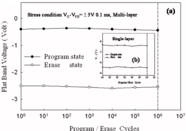
The endurance characteristics of multilayer NCs and single-layer NCs are provided in Fig. 7. Pulse conditions of VG− VFB=⫾5 V for 0.1 ms were applied to evaluate
endur-ance characteristics for the program/erase cycle operations.
In the endurance test, first, we used this pulse condition to stress our samples and then programmed to a program state or erased to an erase state. After that, we used the read mode to detect the flatband voltage, VFB 共read mode: The VFBis
obtained by comparing the C-V curves from a charged state or a quasineutral state.兲. Figures7共a兲and7共b兲both show the negligible degradation of memory window up to 106 p/e cycles for the multilayer and single-layer structure.
In the endurance test, our proposed memory structures had the advantages for the nonvolatile memory application.
Further analysis of the reliability indicated the charge retention properties of single-layer and multilayer NC memory structures at 27 and 85 ° C, which are demonstrated in Figs.8共a兲and8共b兲, respectively. Here, we purposely kept the same memory window, and this measurement results were carried out using a fixed gate voltage stress of ⫾5 V 共10 and 2 ms for single layer and multilayer兲 at 27 and 85 ° C. Hence, the shift in the flatband voltage as a function of time is obtained by comparing the C-V curves. From Fig.
8共a兲, we used an extrapolation to give a long-term predict-able result共solid and dotted line兲 after 1000 s 共stable region
FIG. 3. 共Color online兲 共a兲 N 1s XPS analysis of the NCs 共empty circles and straight line indicate experi-mental and fitting results, respectively兲 and 共b兲 XRD analysis of the NCs共control sample is only Si substrate with tunnel oxide兲 under different thermal annealing temperatures of 300, 500, and 600 ° C.
FIG. 4. 共Color online兲 Cross-sectional TEM analysis and memory cell pro-cess flow of multilayer NCs. The first deposited NC layer was separated into two layers, and this phenomenon was caused by a partial NiSi NCs diffusing into SiNxduring the second RTA process.
FIG. 5. Capacitance-voltage共C-V兲 hystereses of memory structure with 共a兲 single-layer and共b兲 multilayer NCs. The memory windows of 共a兲 5 and 共b兲 13 V can be obtained under⫾10 gate voltage operation, respectively.
of retention兲.15
We find that single-layer and multilayer NiSi NCs all have good chare storage ability and get up to 10 years at room temperature, as shown in Fig.8共a兲.
However, a serious condition of 85 ° C can show the advantages of multilayer NiSi NC memory, and it is found
that the charge loss ratio of a multilayer is much lower than single-layer NCs. In this study, we found that the leakage currents of single- and multilayer NC memories were very small. Therefore, the blocking oxide was enough to block the stored electrons leaking into the Al gate. If the stored elec-tron loss is due to lateral migration effect, the retention test of single- and multilayer NC memories under 85 ° C will have the same results. The biggest difference between single-and multilayer NC memory is the position of main stored carriers. The position of main stored carriers for only single-layer NC memory is like the first NC single-layer of multisingle-layer NC memory. However, the position of main stored carriers for multilayer NC memory is the third NC layer.
Hence, based on the TEM images, we established an energy band diagram of multilayer NCs embedded in SiNx layer共as shown in Fig.9兲 to consider that the reason was due
to the charges stored in the upper-layer NCs共the third layer of multilayer structure兲, which can be suppressed from leak-ing into substrate under thermal test by the Coulomb block-ade effect and energy level quantization of the lower-layer NCs 共the first and second layers of the multilayer structure兲.16,17
The Coulomb blockade effect was caused by the carriers existing in second layer NCs 共as shown in the
FIG. 6. 共Color online兲 Simulation results of electric field distribution of 共a兲 single-layer and 共b兲 multilayer NiSi NCs embedded in nitride layer. Vertical electric field distribution comparisons of共c兲 black dashed line 共across NCs兲 and 共d兲 red dashed line 共without any NCs兲 for the single-layer and multilayer NiSi NCs.
FIG. 7. 共Color online兲 Endurance characteristics of 共a兲 multilayer NiSi NC memory and 共b兲 single-layer NiSi NC memory. Pulse conditions of VG
− VFB=⫾5 V and 0.1 ms.
094303-4 Chen et al. J. Appl. Phys. 104, 094303共2008兲
second layer of energy band diagram兲, and this stored charge reduced the electron loss probability from the third layer to the first layer. In addition, the energy level quantization of NCs is limited to the size and effective mass of a NC. by the
theoretical simulation of Guan et al.17Hence, in this model, the ground states 共Fermi level兲 of first and second layers of the multilayer structure were higher than the third layer be-cause their NC size was smaller than 3 nm. This Fermi level shift can partially suppress the electrons stored in the third NC layer from leaking into the first and second NC layers under thermal test. We also depicted this physical phenom-enon in Fig. 9 to appear that the nonvolatile multilayer nickel-silicide NC memory can effectively keep carriers in the charge trapping layer for a harsh environment.
IV. CONCLUSION
In this study we adopted the Ni–Si–N thin film to easily fabricate the NiSi NCs embedded in SiN layer after a RTA process and also proposed a nonvolatile NiSi NC memory with multilayer using low thermal budget. This multilayer NC structure exhibited superior memory performance for the charge storage capacity and reliability than single-layer NC sample. A larger memory window of 13 V was clearly ob-served after⫾10 V voltage sweep and the retention can get up to 10 years for next-generation nonvolatile memory ap-plication. We also provided an energy band diagram of the multilayer NC structure to display the predominance of NMLNCM at scaling down process. In addition, this forma-tion technique of charge trapping structure was also suitable for the low temperature substrate on the flexible electronics application.
ACKNOWLEDGMENTS
This work was performed at National Nano Device Laboratory and was supported by the National Science Council of the Republic of China under Contract Nos. NSC 96-2221-E-009-202-MY3, NSC 96-2112-M-110-013, and NSC 97-3114-M-110-001.
1S. Tiwari, F. Rana, K. Chan, H. Hanafi, W. Chan, and D. Buchanan, Tech. Dig. - Int. Electron Devices Meet. 1995, 521.
2J. D. Blauwe, IEEE Trans. Nanotechnol. 1, 72共2002兲.
3W. R. Chen, T. C. Chang, P. T. Liu, P. S. Lin, C. H. Tu, and C. Y. Chang, Appl. Phys. Lett.90, 112108共2007兲.
4M. Shalchian, J. Grisolia, G. Ben Assayag, H. Coffin, S. M. Atarodi, and A. Claverie,Appl. Phys. Lett.86, 163111共2005兲.
5W. Guan, S. Long, Q. Liu, Y. Hu, Z. Li, and R. Jia,Solid-State Electron. 51, 806共2007兲.
6J. H. Chen, Y. Q. Wang, W. J. Yoo, Y.-C. Yeo, G. Samudra, D. S. H. Chan, A. Y. Du, and D.-L. Kwong, IEEE Trans. Electron Devices 51, 1840 共2004兲.
7C. Y. Ng, T. P. Chen, L. Ding, and S. Fung,IEEE Electron Device Lett.27, 231共2006兲.
8C. D. Wagner, W. M. Riggs, L. E. Davis, J. F. Moulder, and G. E. Muilen-berg, Handbook of X-Ray Photoelectron Spectroscopy 共Perkin-Elmer, Eden Prairie, MN, 1975兲, p. 298.
9D. R. Lide, CRC Handbook of Chemistry and Physics, 81st ed.共CRC, Boca Raton, FL, 2000兲, Vol. 81, pp. 5–3.
10M. C. Poon, C. H. Ho, F. Deng, S. S. Lau, and H. Wong,Microelectron. Reliab.38, 1495共1998兲.
11W. R. Chen, T. C. Chang, P. T. Liu, C. H. Tu, F. W. Chi, S. W. Tsao, and C. Y. Chang, Surf. Coat. Technol. 202, 1292共2007兲.
12T. C. Chang, S. T. Yan, P. T. Liu, C. H. Hsu, M. T. Tang, and S. M. Sze, Appl. Phys. Lett.84, 2581共2004兲.
FIG. 8.共Color online兲 Retention characteristics of the NC memory structure with共a兲 room temperature, 27 °C, and 共b兲 85 °C. The dotted line and solid line are the extrapolated values of retention data after 1000 s; this range is a steady state.
FIG. 9. Energy bond diagram of multilayer NiSi NCs embedded in SiNx.
The ground states of first and second layers of multilayer structure were caused by the energy level quantization effect.
13S. K. Samanta, P. K. Singh, W. J. Yoo, G. Samudra1, Y.-C. Yeo, L. K. Bera, and N. Balasubramanian, Tech. Dig. - Int. Electron Devices Meet. 2005, 170.
14Z. Liu, C. Lee, V. Narayanan, G. Pei, and E. C. Kan,IEEE Trans. Electron Devices49, 1606共2002兲.
15W. R. Chen, T. C. Chang, P. T. Liu, J. L. Yen, C. H. Tu, J. C. Lou, C. F. Yeh, and C. Y. Chang,Appl. Phys. Lett.91, 082103共2007兲.
16T. Takagahara and K. Takeda,Phys. Rev. B46, 15578共1992兲.
17W. Guan, S. Long, M. Liu, Q. Liu, Y. Hu, Z. Li, and R. Jia,Solid-State Electron.51, 806共2007兲.
094303-6 Chen et al. J. Appl. Phys. 104, 094303共2008兲