Research Article
Gold Nanoparticle-Graphene Oxide Nanocomposites That
Enhance the Device Performance of Polymer Solar Cells
Ming-Kai Chuang,
1Fang-Chung Chen,
1and Chain-Shu Hsu
21Department of Photonics and Institute of Display, National Chiao Tung University, Hsinchu 30010, Taiwan 2Department of Applied Chemistry, National Chiao Tung University, Hsinchu 30010, Taiwan
Correspondence should be addressed to Fang-Chung Chen; [email protected]
Received 25 June 2014; Revised 5 September 2014; Accepted 11 September 2014; Published 14 October 2014 Academic Editor: K. R. Justin Thomas
Copyright © 2014 Ming-Kai Chuang et al. This is an open access article distributed under the Creative Commons Attribution License, which permits unrestricted use, distribution, and reproduction in any medium, provided the original work is properly cited.
Metal nanoparticle-decorated graphene oxides are promising materials for use in various optoelectronic applications because of their unique plasmonic properties. In this paper, a simple, environmentally friendly method for the synthesis of gold nanoparticle-decorated graphene oxide that can be used to improve the efficiency of organic photovoltaic devices (OPVs) is reported. Here, the amino acid glycine is employed as an environmentally friendly reducing reagent for the reduction of gold ions in the graphene oxide solutions. Transmission electron microscopy, atomic force microscopy, X-ray photoelectron spectroscopy, UV-Vis spectroscopy, and Raman spectroscopy are used to characterize the material properties of the resulting nanomaterials. Furthermore, these nanocomposites are employed as the anode buffer layer in OPVs to trigger surface plasmonic resonance, which improved the efficiency of the OPVs. The results indicate that such nanomaterials appear to have great potential for application in OPVs.
1. Introduction
Organic photovoltaic devices (OPVs) have several attractive properties, including light weight, mechanical flexibility, short energy payback times, and fabrication at low cost and low temperature [1–6]. Recently, through intensive research efforts, the cell efficiencies of OPVs have broken through 10% [6]. Nevertheless, further efforts will be needed to improve their power conversion efficiencies (PCEs) to even higher levels and to ensure greater module reliability if these devices are ever to realize their industrialization. Although the internal quantum efficiency (IQE) of state-of-the-art OPVs has approached almost 100% [7], the device thickness of the photoactive layer is limited at approximately 100 nm, meaning that it usually cannot absorb all of the incident photons due to the low mobility of the charge carriers through the organic materials and the high level of charge recombina-tion. Such insufficient absorption becomes a bottleneck that prevents the ability to achieve simultaneously high charge collection and high absorption efficiencies. Therefore, many light-trapping strategies, including the use of optical spacers
[8, 9], diffraction gratings [10], and folded device architec-tures [11, 12], have been explored to improve the degree of light harvesting without affecting the charge collection efficiency.
More recently, there has been a growing interest in using the plasmonic effect of metal nanoparticles (NPs) in OPVs to enhance their light harvesting efficiencies [13–21]. As-synthesized NPs can be incorporated readily into either the buffer [17–21] or photoactive [15, 16] layer during the preparation of OPVs without the need for complicated nanofabrication tools. The localized surface plasmon res-onance (LSPR) effect induced by the NPs can effectively enhance the device absorption efficiency and increase the level of exciton generation, resulting in higher device PCEs. Because direct blending of metal NPs with the photoac-tive layer can affect the morphology, the metal NPs are frequently positioned within device buffer layers, such as poly(3,4-ethylenedioxythiophene):polystyrene sulfonate (PEDOT:PSS) [17,18]. Nevertheless, the use of PEDOT:PSS as the matrix can result in several problems arising from the material’s highly acidic and hygroscopic properties [22].
Volume 2014, Article ID 736879, 12 pages http://dx.doi.org/10.1155/2014/736879
As an alternative to PEDOT:PSS, Li et al. recently employed solution-processable graphene oxides (GOs) as hole buffer layers in OPVs and achieved respectable device efficiencies [23]. In addition, reduced GOs (rGOs) have been also used as the buffer layers to improve the device stability [24]. Because of their unique properties on the nanoscale, these nanosheets, including graphene, GOs, and their derivatives, have been considered as a promising mate-rial platform for improving the performance of OPVs [23–
27].
Many proposed methods for the synthesis of metal NPs and rGOs employ hazardous and highly toxic reducing agents, including hydrazine, sodium borohydrate, and their derivatives [28–31]. To achieve greener syntheses, several environmentally friendly reducing agents, including ascorbic acid [32, 33], glycine [34], reducing sugars [35], and mela-tonin [36], have also been introduced for the preparation of rGOs. Among these environmentally friendly reducing agents, glycine is the smallest and simplest essential amino acid for humans and is commonly found in proteins [34]. Previously, Bose et al. found that glycine can reduce GO successfully to produce graphene; it can also function as a chemical stabilizing reagent for achieving admirable aqueous dispersibility [34]. More recently, we have developed gold nanoparticle/graphene oxide (AuNP-GO) nanocomposites for triggering LSPR in polymer solar cells [37]. In this present study, we further employed the amino acid glycine as an environmentally friendly reducing reagent for the synthesis of AuNP-GO nanocomposites, which were then used in OPVs. Comparing with the previous work [37], the one-pot synthesis approach in this study simplified the material preparation; no further capping agent was required for preventing the aggregation of the nanoparticles. We investigated the optical effects of the LSPRs on the device performance, observing enhancements in both photocurrent and overall device efficiency. Because of their promising biological compatibility, these nanocomposites appear to have great potential for applications not only in energy har-vesting devices but also in OPV-based biomedical treatments [38].
2. Experimental Methods
2.1. Synthesis of AuNP-GO Composites. The chemical
synthe-sis of the AuNP-GO composites was performed following procedures reported in the literature [34, 39]. An aqueous solution was prepared by mixing GO (0.275 mg/mL, 3 mL) and HAuCl4 (0.047 mg/mL, 10 mL) components and then aged for 30 min. After heating the solution to 80∘C, a solution of a reducing agent, either sodium citrate or glycine, was added. The resulting solution was continuously stirred for 4 h. The as-prepared suspensions were then centrifuged (6000 rpms) and washed with DI water twice to remove the unreacted gold ions. Finally, the nanocomposites were dried through lyophilization.
2.2. Characterization. XPS spectra were recorded using a
PHI 5000 VersaProbe system. The absorption spectrum was
recorded using a UV-Vis-NIR spectrometer (PerkinElmer Lambda 950). The surface morphology of the GO films was obtained using a Digital Instruments Dimension 3100 atomic force microscope. Raman spectra were obtained using a Horoba high-resolution confocal Raman micro-scope.
2.3. Device Fabrication and Testing. The devices were
pre-pared on patterned ITO-coated glass substrates. After per-forming a routine cleaning process, the substrates were dried in an oven for at least 12 h and then treated with UV ozone. To prepare the AuNP-GO films, the concentrations of AuNP-GO and GO were adjusted to 0.110 and 0.165 mg/mL, respectively. The GO or AuNP-GO solutions were spin-coated onto the ITO substrates and then the thin films were baked at 180∘C for 20 min. The photoactive layer, a blend of P3HT (Rieke Metals) and PCBM (Solenne) in 1,2-dichlorobenzene, was spin-coated onto the GO or AuNP-GO layer. The acceptor (PCBM) was also replaced by indene-C60 bisadduct (ICBA), another C60derivative that possesses a higher LUMO energy level [40,41], to improve the open-circuit voltage. The photoactive films also underwent solvent annealing in a glass Petri dish [42]. After subsequent thermal annealing at 110∘C for 15 min, a bilayer cathode comprising Ca (30 nm) and Al (100 nm) was deposited sequentially through thermal evaporation. The completed devices were encapsulated by cover glasses. The electrical characteristics of the devices were acquired using a Keithley 2400 source-measure unit. A 150-W Thermal Oriel solar simulator (AM 1.5 G) was used as the light source to obtain the device performance under illumination conditions. The intensity of the light source was calibrated using a standard Si photodiode equipped with a KG5 filter [43]. The IPCE spectra were obtained with a QE measurement system (Enli Technol-ogy).
3. Results and Discussion
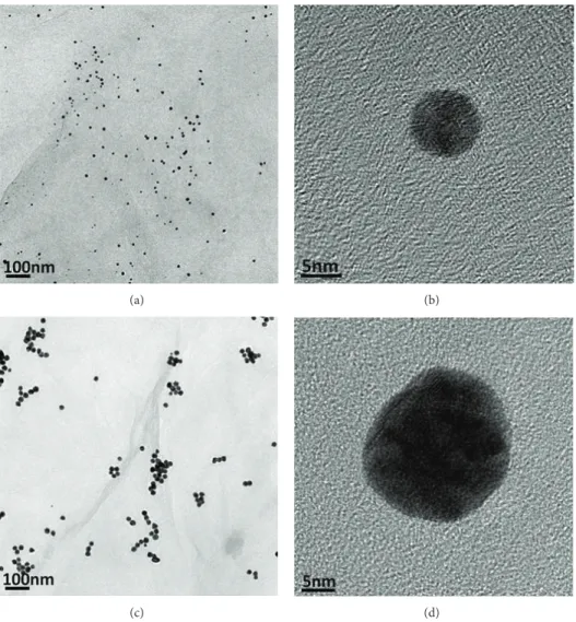
We employed a simple one-pot synthesis to prepare the AuNP-GO nanocomposites [34,39]. In a typical experiment, an aqueous solution containing GO and HAuCl4was heated at 80∘C and then a reducing agent, either glycine or sodium citrate, was added to the stirred solution. A clear color change occurred to the dispersion, suggesting the formation of AuNPs. Notably, the nanomaterials could be dispersed well in water after sonication. Figure 1 displays transmis-sion electron microscopy (TEM) images of the AuNP-GO composites. Hereafter, we denote the AuNP-GO materials obtained using glycine and sodium citrate by AuNP-GO/GL and AuNP-GO/SC, respectively. In the TEM images, we observe some wrinkles from the GO, with NPs anchored to the nanosheets. The distribution of the AuNPs was rather even on the AuNP-GO/GL sheets. In contrast, the AuNPs tended to aggregate in the AuNP-GO/SC composites. We suspect that glycine behaved as a stronger stabilizing reagent and prevented the aggregation of the AuNPs on the GO surface. In addition, high-resolution TEM images (Figures
(a) (b)
(c) (d)
Figure 1: (a, c) TEM and (b, d) high-resolution TEM images of (a, b) AuNP-GO/GL and (c, d) AuNP-GO/SC composites.
average sizes of approximately 7 and 20 nm for the AuNP-GO/GL and AuNP-GO/SC composites, respectively.
Amino acids have been considered as ideal biocompatible capping agents for stabilizing metal NPs [44]. Previously, Pakiari and Jamshidi have studied the interaction of amino acids, including glycine and cysteine, with gold and silver clusters using density functional theory [45]. They concluded that the chemical bonds are partially electrostatic and par-tially covalent. Meanwhile, Hamaguchi et al. also synthesized glycine-stabilized AuNPs and suggested that the unproto-nated amine and carboxylic groups of the glycine moieties interact strongly with Au [46]. In this study, we suspect that such strong affinities between glycine and AuNPs can also help to stabilize the NPs on the GO surfaces. Therefore, the excess of glycine after the reduction step behaved as a capping agent and prevented the aggregation of AuNPs.
We also performed solubility tests of the materials in water; the results were displayed in Figure 2(a). Both the sets of AuNP-GO nanocomposites could be dispersed well after sonication. Nevertheless, we could occasionally observe
some black powder formed after aging for 15 days for the AuNP-GO/SC sample. Although this black powder could be redispersed after gentle shaking of the solution, precipitates appeared after 40 days that could not be redispersed readily. In contrast, the AuNP-GO/GL solution exhibited higher solubility; the solution remained clear after aging for 40 days [34,47].
Color changes occurred to the solutions during the syntheses of both sets of AuNP-GO materials. The resulting colors were, however, slightly different for the two types of nanocomposites (Figure 2(a)). The UV-Vis absorption spectra in Figure 2(b) reveal a peak near 580 nm for the AuNP-GO/GL composites; this signal corresponds to the plasmonic absorption of the AuNPs. In contrast, the spec-trum of the AuNP-GO/SC composite exhibited an absorption peak near 550 nm. The different locations of the plasmonic bands may have originated from the different surface coatings on the NPs, resulting in different dielectric environments [48, 49]. Furthermore, the two solutions also exhibited typical extinction peaks for GOs at 230 and 305 nm, which
(a) 200 400 600 800 N o rm al iz ed a b so rp ti o n Wavelength (nm) AuNP-GO/GL AuNP-GO/SC GO 450 500 550 600 650 Wavelength (nm) (b)
Figure 2: Characteristics of AuNP/GO nanocomposites. (a) Photograph of aqueous dispersions of the AuNP/GO nanocomposites. (Left) AuNP-GO/SC dispersion after aging for 40 days; (middle) as-prepared AuNP-GO/SC solution; (right) AuNP-GO/GL dispersion after aging for 40 days. (b) UV-Vis absorption spectra of GO and AuNP-GO nanocomposites in water.
1200 1400 1600 1800 In te n si ty (a.u .) GO AuNP-GO/SC AuNP-GO/GL Raman shift (cm−1)
Figure 3: Raman spectra of GO and the nanocomposites.
correspond to the𝜋-𝜋∗ transitions of C=C bonds and the 𝑛-𝜋∗ transitions of C=O groups, respectively [50]. Because
these two characteristic peaks had not shifted, we suspected that the chemical structures of the GO sheets had not changed too much or that they had been reduced only mildly during the reduction processes.
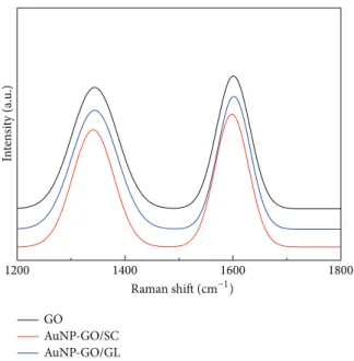
To further investigate the structural changes of the GO materials, we performed Raman spectroscopic measure-ments (Figure 3). The Raman spectra of the pure GO and
the AuNP-GO materials all featured a typical D band at 1342 cm−1 (breathing mode of sp2-hybridized C atoms in rings) and a G band at 1599 cm−1 (in-plane bond stretching of sp2-hybridized C atoms) [36, 51]. Because the D band is usually associated with structural defects induced by the presence of OH and/or epoxide groups on the basal plane, the ratio of the intensities of the D and G bands (𝐼D/𝐼G) is often
used to measure the extent of disorder. The𝐼D/𝐼Gratio for our
sample of GO was 0.91; it decreased slightly to 0.88 and 0.90 for the AuNP-GO/SC and AuNP-GO/GL composites, respec-tively. Thus, the GO nanosheets were presumably reduced only slightly during the reduction processes, consistent with the previous data of UV-Vis absorption measurements.
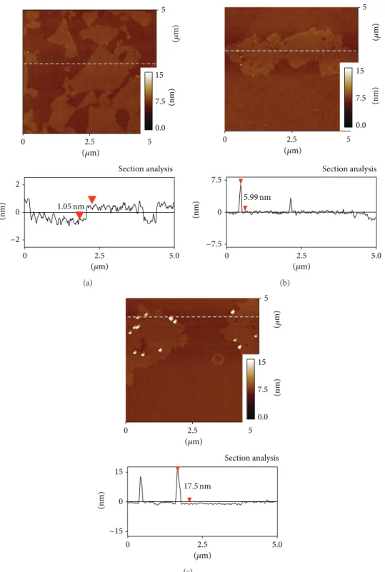
Figure 4displays atomic force microscopy (AFM) images of the GO derivatives deposited on SiO2 surfaces. In
Figure 4(a), we clearly observe individual single-layer GO sheets having lateral dimensions of several hundred to thou-sand of nanometers. The height profile diagram in the image indicates a thickness of approximately 1.0 nm, consistent with the typical thicknesses reported previously [36,52,53]. The AFM images of the AuNP-GO/GL and AuNP-GO/SC composites (Figures4(b)and4(c), resp.) both reveal AuNPs adhered to the GO surfaces. We could roughly estimate the dimensions of the NPs from these AFM images. The AuNPs formed on the GO sheets when using sodium citrate had an average size of 18 nm, significantly larger than that of the NPs prepared using glycine (ca. 6 nm). Furthermore, the AFM images indicate that the distribution of the AuNPs in the AuNP-GO/GL composite was rather uniform, whereas some aggregation was evident in the AuNP-GO/SC sample. Overall, the AFM results confirm the conclusions drawn from the TEM images.
0 (nm) 2.5 5 5 (𝜇m) (𝜇m) (𝜇 m) 15 7.5 0.0 (nm) 0 2.5 5.0 Section analysis 1.05 nm 2 0 −2 (a) (nm) 5 0 2.5 5 (𝜇m) (𝜇 m) 15 7.5 0.0 (nm) (𝜇m) 0 2.5 5.0 Section analysis 7.5 0 −7.5 5.99 nm (b) 5 0 2.5 5 (𝜇m) (𝜇 m) 15 7.5 0.0 (nm) 15 0 −15 Section analysis 17.5 nm (nm) (𝜇m) 0 2.5 5.0 (c)
Figure 4: AFM topographic images of (a) GO, (b) AuNP-GO/GL, and (c) AuNP-GO/SC on SiO2substrates. The bottom figures display the
corresponding AFM height profiles. Vertical distances between the markers are noted in the height diagrams.
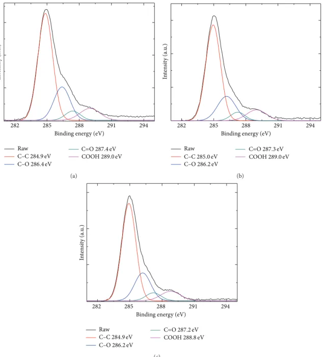
X-ray photoelectron spectroscopy (XPS) is a quantitative spectroscopic technique that can probe the electronic states of the elements comprising a material.Figure 5displays the C 1s XPS characteristics of our GO composites. Four typical deconvoluted peaks appeared in the spectrum of the GO [34,39]; we attribute the peak at 284.9 eV to the C–C and C=C
bonds in the aromatic rings and the other three, centered at 286.4, 287.4, and 289.0 eV, to the C–O units of epoxy and/or alkoxy, C=O, and O=C–OH groups, respectively. Upon reduction with sodium citrate or glycine, the peaks shifted slightly, suggesting a small perturbation in the bonding of the C atoms. More importantly, the intensity of the signals for
282 285 288 291 294 In te n si ty (a.u .)
Binding energy (eV) Raw C–C284.9 eV C–O286.4 eV C=O 287.4 eV COOH289.0 eV (a) I n te n si ty (a.u .) 282 285 288 291 294
Binding energy (eV) Raw C–C285.0 eV C–O286.2 eV C=O 287.3 eV COOH289.0 eV (b) In te n si ty (a.u .) 282 285 288 291 294
Binding energy (eV) Raw C–C284.9 eV C–O286.2 eV C=O 287.2 eV COOH288.8 eV (c)
Figure 5: C 1s XPS spectra of (a) GO, (b) AuNP-GO/SC, and (c) AuNP-GO/GL composites.
the C–C and C=C bonds increased, suggesting the removal of functional groups containing oxygen atoms. Again, these results suggest that the GO sheets of the nanocomposites were reduced slightly. The peak area (𝐴) ratios of the signals for the oxygen-containing and C–C/C=C bonds are listed inTable 1. The XPS data confirm that both of the tested reducing agents modified the GO nanosheets only slightly.
To investigate the plasmonic effects of these nanocompos-ites on the performance of OPVs, we fabricated devices using various GO derivatives as anode buffer layers. Direct use of the as-synthesized AuNP-GO composites resulted in poor device performance, presumably because of strong backscat-tering by the AuNPs. Therefore, we diluted the solution
Table 1: Peak area (A) ratios of oxygen-containing bonds to the C– C/C=C bonds, determined from XPS data.
Sample GO AuNP-GO/GL AuNP-GO/SC
𝐴C–O/𝐴CC 0.344 0.318 0.329
𝐴C=O/𝐴CC 0.088 0.087 0.086
𝐴COOH/𝐴CC 0.152 0.152 0.135
with neat GO and blended the aqueous mixture with MeOH to improve the film quality; the resulting H2O-to-MeOH volume ratio was 1 : 2.Figure 6displays the reflection spectra of the resulting films prepared before and after the dilution,
Table 2: Electrical characteristics of devices fabricated with GO and various AuNP-GO nanocomposites as the anode buffer layers.
Device 𝑉oc(V) 𝐽sc(mA cm−2) FF PCE (%)
GOa 0.57± 0.02 9.24± 0.42 0.64± 0.02 3.34± 0.13
AuNP-GO/GLa 0.57± 0.02 10.70± 0.42 0.64± 0.02 3.89± 0.15
AuNP-GO/SCa 0.53± 0.02 8.56± 0.50 0.62± 0.02 2.82± 0.18
GOb 0.82± 0.01 8.44± 0.19 0.60± 0.02 4.12± 0.13
AuNP-GO/GLb 0.82± 0.01 10.60± 0.21 0.59± 0.02 5.10± 0.06
aPhotoactive materials: P3HT and PCBM;bphotoactive materials: P3HT and ICBA.
400 500 600 700 800 1 2 3 4 5 6 Refle ct an ce (%) Wavelength (nm) Before After dilution
Figure 6: The reflection spectra of the films prepared before and after dilution. The sample structure was ITO/AuNP-GO compos-ites/P3HT:PCBM. The light was illumined from the ITO side.
respectively. Apparently, the reflectance values decreased after we diluted the solution, especially within the spectral range from 400 to 660 nm. The higher density of AuNPs might lead to stronger reflectance.
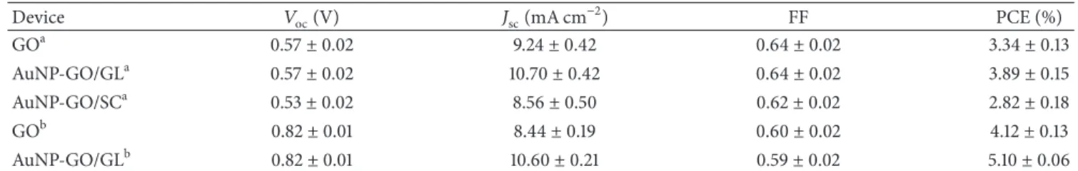
Figure 7(a) displays the current density-voltage (J-V) characteristics of the OPV devices incorporating the GO derivatives under illumination at 100 mW cm−2 (AM1.5G); the photovoltaic parameters are summarized in Table 2. The device prepared with neat GO exhibited an open-circuit voltage (𝑉oc) of 0.57 V, a short-circuit current (𝐽sc)
of 9.24 mA cm−2, and a fill factor (FF) of 0.64, yielding a PCE of 3.37%.Figure 7(a)andTable 2reveal that the device performance improved after incorporating AuNP-GO/GL as the anode buffer layer. For the optimized device, the value of 𝐽scincreased to 10.70 mA cm−2and the value of𝑉ocremained
unchanged (0.57 V), suggesting that the anodic interface was not affected; as a result, the PCE improved to 3.89%. For the device incorporating the AuNP-GO/SC nanocomposites, the value of 𝑉oc decreased to 0.53 V, suggesting significant
deterioration of the anodic interface. The lower values of𝐽sc
(8.56 mA cm−2) and FF (0.62) also indicated that the interface was affected after decorating the GO surfaces with the AuNPs. The solubility of the AuNP-GO/SC nanocomposites was apparently lower than that of the AuNP-GO/GL materials,
as noted in Figure 2. The lower stability of the solution presumably led to device buffer layers having inferior film quality, resulting in poorer device performance.
To study the mechanism of the improvement in perfor-mance, we measured the incident photon-to-electron conver-sion efficiency (IPCE) spectra (Figure 7(b)). The efficiencies improved for the AuNP-GO/GL device, consistent with the
J-V characteristics. For comparison,Figure 7(c)displays the plot of the increase in IPCE (ΔIPCE) with respect to the absorption spectrum of AuNP-GO/GL. The photocurrent increased at wavelengths in the range from 450 to 650 nm, coinciding with the extinction range of the AuNPs. These results reveal that the LSPR effects should be responsible for the improved device performance [18,37].
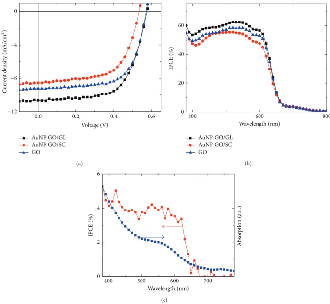
To investigate the plasmonic effect, we performed steady-state photoluminescence (PL) measurements using a 470 nm laser as the excitation source (Figure 8) after spin-coating pristine P3HT films onto GO- and AuNP-GO/GL-modified indium tin oxide (ITO) substrates. The integrating PL inten-sity of the AuNP-GO/GL sample was enhanced relative to that of the GO sample, implying an increase in exciton generation in P3HT upon excitation of the LSPRs. Because the resonance peak of the AuNPs was close to the absorption band of P3HT, the higher PL intensity was probably due to the higher
0.0 0.2 0.4 0.6 0 Voltage (V) AuNP-GO/GL AuNP-GO/SC GO −12 −8 −4 C u rr en t den si ty (mA/cm 2) (a) 400 600 0 20 40 60 IPCE (%) Wavelength (nm) AuNP-GO/GL AuNP-GO/SC GO 800 (b) 400 500 600 700 0 2 4 6 Wavelength (nm) IPCE (%) A b so rp tio n (a.u .) (c)
Figure 7: (a) J-V characteristics, recorded under illumination at 100 mW cm−2(AM1.5G), of polymer solar cells incorporating GO and
AuNP-GO composites; the active materials were P3HT and PCBM. (b) Corresponding IPCE curves of these OPV devices. (c) Plot of difference in IPCE (ΔIPCE) after incorporating the AuNP-GO anode buffer layer; the absorption spectrum of the AuNP-GO/GL composite provided for comparison.
level of light absorption in the active layer, suggesting that the enhanced local electromagnetic field increased the total number of excitons [18,37].
We have also prepared rGOs using glycine as the reducing agent. Without the presence of gold ions, we found that the GOs could be reduced, which was consistent with the previous literature [34]. From the Raman spectra (the inset toFigure 9), we could see the𝐼D/𝐼G ratio was increased to
1.36, suggesting the reduction of GOs. Then, we fabricated devices using the resulting rGOs as the anode buffer layers; the J-V curve is shown in Figure 9. The device exhibited a 𝑉oc of 0.55 V, a 𝐽sc of 8.93 mA cm−2, and a FF of 0.61;
the calculated PCE was 3.00%. Apparently, the photocur-rent was reduced compared with that of the GO device.
Thus, the device results did not reveal the increment of transport properties due to the better conductance of the GO films. It might be due to the decreased solubility of the rGOs, which could result in inferior film quality under our fabrication conditions. Therefore, we rule out the pos-sibility that the performance enhancement is due to the increment of transport properties by reducing of GOs and mainly contribute the performance enhancement to the LSPR effects.
The value of𝑉ocof an OPV device is closely related to the
energy difference between the highest occupied molecular orbital (HOMO) of its polymer donors and the lowest unoccupied molecular orbital (LUMO) of its fullerenes [40,
500 600 700 800 900 100 200 300 400 PL in te n si ty (a.u .) Wavelength (nm) GO AuNP-GO/GL Excitation source:470 nm
Figure 8: PL spectra of the GO and AuNP-GO/GL samples recorded using an excitation wavelength (𝜆exc) of 470 nm.
0.0 0.1 0.2 0.3 0.4 0.5 0.6 0 Voltage (V) GO rGO 1000 1200 1400 1600 1800 2000 800 1600 2400 In te n si ty (a.u .) rGO Raman shift (cm−1) −10 −8 −6 −4 −2 C u rr en t den si ty (mA/cm 2 )
Figure 9: J-V characteristics of the devices prepared with GOs or rGOs as the anodic buffer under illumination at 100 mW cm−2(AM1.5G).
The inset displays the Raman spectrum of the rGO thin film.
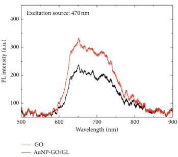
PCBM, we replaced the PCBM component with ICBA to increase the photovoltage [40,41].Figure 10(a)displays the
J-V characteristics of devices prepared using a P3HT:ICBA
blend as the photoactive layer. The device incorporating the neat GO exhibited a 𝑉oc value of 0.82 V, a 𝐽sc a value of
8.44 mA cm−2, and a FF value of 0.60, yielding a PCE value of 4.12%. After decorating the GO with AuNPs, the value of 𝐽scimproved significantly to 10.60 mA cm−2, while the value
of𝑉ocremained unchanged, causing the PCE to increase to
5.10%. As shown in Figure 10(b), the IPCE spectra of the P3HT:ICBA-based devices exhibited trends similar to that of the photocurrent. Thus, AuNP-GO composites appear to have great potential for use in OPVs containing various photoactive materials.
4. Conclusions
We have demonstrated an environmentally friendly method for synthesizing nanocomposites from AuNPs and GOs through a simple one-pot reaction. Compared with our pre-vious work [37], we found that no further capping agent was required for preventing the aggregation of the nanoparticles. Because glycine simultaneously serves as the reducing and the capping agent, the synthesis route has been simplified. We have used TEM, AFM, XPS, UV-Vis spectroscopy, and Raman spectroscopy to characterize the material properties of these nanomaterials, which we further employed as hole buffer layers in OPVs. More importantly, when the GO surface was modified with AuNPs, we observed improved
0.0 0.2 0.4 0.6 0.8 0 Voltage (V) GO AuNP-GO/GL −12 −8 −4 C u rr en t den si ty (mA/cm 2 ) (a) 400 500 600 700 800 0 20 40 60 80 IPCE (%) Wavelength (nm) GO AuNP-GO/GL (b)
Figure 10: (a) J-V characteristics of polymer solar cells fabricated with GO and AuNP-GO/GL composites under illumination at 100 mW cm−2
(AM1.5G); the electron acceptor was ICBA. (b) The corresponding IPCE curves of OPV devices incorporating GO and AuNP-GO/GL as anodic buffer layers.
device performances, due to surface plasmonic effects. Such AuNP-GO nanomaterials appear to have great potential for application in OPVs and OPV-based biomedical treatments.
Conflict of Interests
The authors declare that there is no conflict of interests regarding the publication of this paper.
Acknowledgments
The authors thank the Ministry of Science and Technology (Grant nos. NSC 103-2923-E-009-001-MY3, NSC 102-2221-E-009-130-MY3, and NSC 101-2628-E-009-008-MY3) and the Ministry of Education of Taiwan (through the ATU program) for financial support.
References
[1] G. Dennler, M. C. Scharber, and C. J. Brabec, “Polymer-fullerene bulk-heterojunction solar cells,” Advanced Materials, vol. 21, no. 13, pp. 1323–1338, 2009.
[2] L.-M. Chen, Z. Hong, G. Li, and Y. Yang, “Recent progress in polymer solar cells: manipulation of polymer: fullerene morphology and the formation of efficient inverted polymer solar cells,” Advanced Materials, vol. 21, no. 14-15, pp. 1434–1449, 2009.
[3] H.-L. Yip and A. K.-Y. Jen, “Recent advances in solution-processed interfacial materials for efficient and stable polymer solar cells,” Energy and Environmental Science, vol. 5, no. 3, pp. 5994–6011, 2012.
[4] J. D. Servaites, M. A. Ratner, and T. J. Marks, “Organic solar cells: a new look at traditional models,” Energy and Environmental Science, vol. 4, no. 11, pp. 4410–4422, 2011.
[5] A. L. Roes, E. A. Alsema, K. Blok, and M. K. Patel, “Ex-ante envi-ronmental and economic evaluation of polymer photovoltaics,” Progress in Photovoltaics: Research and Applications, vol. 17, no. 6, pp. 372–393, 2009.
[6] M. A. Green, K. Emery, Y. Hishikawa, W. Warta, and E. D. Dunlop, “Solar cell efficiency tables (version 43),” Progress in Photovoltaics: Research and Applications, vol. 22, no. 1, pp. 1–9, 2014.
[7] S. H. Park, A. Roy, S. Beaupr´e et al., “Bulk heterojunction solar cells with internal quantum efficiency approaching 100%,” Nature Photonics, vol. 3, no. 5, pp. 297–303, 2009.
[8] J. Y. Kim, S. H. Kim, H.-H. Lee et al., “New architecture for high-efficiency polymer photovoltaic cells using solution-based titanium oxide as an optical spacer,” Advanced Materials, vol. 18, no. 5, pp. 572–576, 2006.
[9] F.-C. Chen, J.-L. Wu, and Y. Hung, “Spatial redistribution of the optical field intensity in inverted polymer solar cells,” Applied Physics Letters, vol. 96, no. 19, Article ID 193304, 2010. [10] B. Cocilovo, A. Amooali, A. Lopez-Santiago et al., “Effect of
modular diffraction gratings on absorption in P3HT:PCBM layers,” Applied Optics, vol. 52, no. 5, pp. 1025–1034, 2013. [11] K. Tvingstedt, V. Andersson, F. Zhang, and O. Ingan¨as, “Folded
reflective tandem polymer solar cell doubles efficiency,” Applied Physics Letters, vol. 91, no. 12, Article ID 123514, 2007.
[12] Y. Zhou, F. Zhang, K. Tvingstedt, W. Tian, and O. Ingan¨as, “Multifolded polymer solar cells on flexible substrates,” Applied Physics Letters, vol. 93, no. 3, Article ID 033302, 2008.
[13] C. H. Chou and F. C. Chen, “Plasmonic nanostructures for light trapping in organic photovoltaic devices,” Nanoscale, vol. 6, pp. 8444–8458, 2014.
[14] K. D. G. I. Jayawardena, L. J. Rozanski, C. A. Mills, M. J. Beliatis, N. A. Nismy, and S. R. P. Silva, “‘Inorganics-in-Organics’: recent developments and outlook for 4G polymer solar cells,” Nanoscale, vol. 5, no. 18, pp. 8411–8427, 2013.
[15] D. H. Wang, K. H. Park, J. H. Seo et al., “Enhanced power conversion efficiency in PCDTBT/PC 70 BM bulk heterojunc-tion photovoltaic devices with embedded silver nanoparticle clusters,” Advanced Energy Materials, vol. 1, no. 5, pp. 766–770, 2011.
[16] X. Li, W. C. H. Choy, H. Lu, W. E. I. Sha, and A. H. P. Ho, “Efficiency enhancement of organic solar cells by using shape-dependent broadband plasmonic absorption in metallic nanoparticles,” Advanced Functional Materials, vol. 23, no. 21, pp. 2728–2735, 2013.
[17] F.-C. Chen, J.-L. Wu, C.-L. Lee, Y. Hong, C.-H. Kuo, and M. H. Huang, “Plasmonic-enhanced polymer photovoltaic devices incorporating solution-processable metal nanoparti-cles,” Applied Physics Letters, vol. 95, no. 1, Article ID 013305, 2009.
[18] J.-L. Wu, F.-C. Chen, Y.-S. Hsiao et al., “Surface plasmonic effects of metallic nanoparticles on the performance of polymer bulk heterojunction solar cells,” ACS Nano, vol. 5, no. 2, pp. 959– 967, 2011.
[19] X. Yang, C.-C. Chueh, C.-Z. Li et al., “High-efficiency polymer solar cells achieved by doping plasmonic metallic nanoparticles into dual charge selecting interfacial layers to enhance light trapping,” Advanced Energy Materials, vol. 3, no. 5, pp. 666–673, 2013.
[20] C.-S. Kao, F.-C. Chen, C.-W. Liao, M. H. Huang, and C.-S. Hsu, “Plasmonic-enhanced performance for polymer solar cells prepared with inverted structures,” Applied Physics Letters, vol. 101, Article ID 193902, 2012.
[21] Y.-S. Hsiao, S. Charan, F.-Y. Wu et al., “Improving the light trapping efficiency of plasmonic polymer solar cells through photon management,” Journal of Physical Chemistry C, vol. 116, no. 39, pp. 20731–20737, 2012.
[22] M. Jørgensen, K. Norrman, and F. C. Krebs, “Stability/degrada-tion of polymer solar cells,” Solar Energy Materials and Solar Cells, vol. 92, no. 7, pp. 686–714, 2008.
[23] S.-S. Li, K.-H. Tu, C.-C. Lin, C.-W. Chen, and M. Chhowalla, “Solution-processable graphene oxide as an efficient hole trans-port layer in polymer solar cells,” ACS Nano, vol. 4, no. 6, pp. 3169–3174, 2010.
[24] J.-M. Yun, J.-S. Yeo, J. Kim et al., “Solution-processable reduced graphene oxide as a novel alternative to PEDOT:PSS hole transport layers for highly efficient and stable Polymer solar cells,” Advanced Materials, vol. 23, no. 42, pp. 4923–4928, 2011. [25] X. Liu, H. Kim, and L. J. Guo, “Optimization of thermally
reduced graphene oxide for an efficient hole transport layer in polymer solar cells,” Organic Electronics: physics, materials, applications, vol. 14, no. 2, pp. 591–598, 2013.
[26] J. Liu, Y. Xue, Y. Gao, D. Yu, M. Durstock, and L. Dai, “Hole and electron extraction layers based on graphene oxide derivatives for high-performance bulk heterojunction solar cells,” Advanced Materials, vol. 24, no. 17, pp. 2228–2233, 2012. [27] D. Chen, H. Zhang, Y. Liu, and J. Li, “Graphene and its
deriva-tives for the development of solar cells, photoelectrochemical, and photocatalytic applications,” Energy and Environmental Science, vol. 6, no. 6, pp. 1362–1387, 2013.
[28] D. Li, M. B. M¨uller, S. Gilje, R. B. Kaner, and G. G. Wallace, “Processable aqueous dispersions of graphene nanosheets,” Nature Nanotechnology, vol. 3, no. 2, pp. 101–105, 2008. [29] S. Park and R. S. Ruoff, “Chemical methods for the production
of graphenes.,” Nature nanotechnology, vol. 4, no. 4, pp. 217–224, 2009.
[30] G. Wang, J. Yang, J. Park et al., “Facile synthesis and character-ization of graphene nanosheets,” Journal of Physical Chemistry C, vol. 112, no. 22, pp. 8192–8195, 2008.
[31] S. Pei, J. Zhao, J. Du, W. Ren, and H.-M. Cheng, “Direct reduction of graphene oxide films into highly conductive and flexible graphene films by hydrohalic acids,” Carbon, vol. 48, no. 15, pp. 4466–4474, 2010.
[32] J. I. Paredes, S. Villar-Rodil, M. J. Fern´andez-Merino, L. Guardia, A. Mart´ınez-Alonso, and J. M. D. Tasc´on, “Environ-mentally friendly approaches toward the mass production of processable graphene from graphite oxide,” Journal of Materials Chemistry, vol. 21, no. 2, pp. 298–306, 2011.
[33] J. Zhang, H. Yang, G. Shen, P. Cheng, J. Zhang, and S. Guo, “Reduction of graphene oxide vial-ascorbic acid,” Chemical Communications, vol. 46, no. 7, pp. 1112–1114, 2010.
[34] S. Bose, T. Kuila, A. K. Mishra, N. H. Kim, and J. H. Lee, “Dual role of glycine as a chemical functionalizer and a reducing agent in the preparation of graphene: an environmentally friendly method,” Journal of Materials Chemistry, vol. 22, no. 19, pp. 9696–9703, 2012.
[35] C. Zhu, S. Guo, Y. Fang, and S. Dong, “Reducing sugar: new functional molecules for the green synthesis of graphene nanosheets,” ACS Nano, vol. 4, no. 4, pp. 2429–2437, 2010. [36] A. Esfandiar, O. Akhavan, and A. Irajizad, “Melatonin as a
powerful bio-antioxidant for reduction of graphene oxide,” Journal of Materials Chemistry, vol. 21, no. 29, pp. 10907–10914, 2011.
[37] M.-K. Chuang, S.-W. Lin, F.-C. Chen, C.-W. Chu, and C.-S. Hsu, “Gold nanoparticle-decorated graphene oxides for plasmonic-enhanced polymer photovoltaic devices,” Nanoscale, vol. 6, no. 3, pp. 1573–1579, 2014.
[38] J.-L. Wu, F.-C. Chen, M.-K. Chuang, and K.-S. Tan, “Near-infrared laser-driven polymer photovoltaic devices and their biomedical applications,” Energy and Environmental Science, vol. 4, no. 9, pp. 3374–3378, 2011.
[39] Z. Zhang, H. Chen, C. Xing et al., “Sodium citrate: a universal reducing agent for reduction/decoration of graphene oxide with au nanoparticles,” Nano Research, vol. 4, no. 6, pp. 599–611, 2011. [40] G. J. Zhao, Y. J. He, and Y. Li, “6.5% efficiency of polymer
solar cells based on poly(3-hexylthiophene) and indene-C60
bisadduct by device optimization,” Advanced Materials, vol. 22, no. 39, pp. 4355–4358, 2010.
[41] Y. J. He, H.-Y. Chen, J. H. Hou, and Y. F. Li, “Indene—C60
bisadduct: a new acceptor for high-performance polymer solar cells,” Journal of the American Chemical Society, vol. 132, no. 4, pp. 1377–1382, 2010.
[42] F.-C. Chen, C.-J. Ko, J.-L. Wu, and W.-C. Chen, “Morphological study of P3HT:PCBM blend films prepared through solvent annealing for solar cell applications,” Solar Energy Materials and Solar Cells, vol. 94, no. 12, pp. 2426–2430, 2010.
[43] V. Shrotriya, G. Li, Y. Yao, T. Moriarty, K. Emery, and Y. Yang, “Accurate measurement and characterization of organic solar cells,” Advanced Functional Materials, vol. 16, no. 15, pp. 2016– 2023, 2006.
[44] S. K. Bhargava, J. M. Booth, S. Agrawal, P. Coloe, and G. Kar, “Gold nanoparticle formation during bromoaurate reduction by amino acids,” Langmuir, vol. 21, no. 13, pp. 5949–5956, 2005. [45] A. H. Pakiari and Z. Jamshidi, “Interaction of amino acids with gold and silver clusters,” Journal of Physical Chemistry A, vol. 111, no. 20, pp. 4391–4396, 2007.
[46] K. Hamaguchi, H. Kawasaki, and R. Arakawa, “Photochemical synthesis of glycine-stabilized gold nanoparticles and its heavy-metal-induced aggregation behavior,” Colloids and Surfaces A: Physicochemical and Engineering Aspects, vol. 367, no. 1–3, pp. 167–173, 2010.
[47] J. Gao, F. Liu, Y. Liu, N. Ma, Z. Wang, and X. Zhang, “Environment-friendly method to produce graphene that employs vitamin C and amino acid,” Chemistry of Materials, vol. 22, no. 7, pp. 2213–2218, 2010.
[48] J. A. Schuller, E. S. Barnard, W. Cai, Y. C. Jun, J. S. White, and M. L. Brongersma, “Plasmonics for extreme light concentration and manipulation,” Nature Materials, vol. 9, article 368, 2010. [49] H. A. Atwater and A. Polman, “Plasmonics for improved
photovoltaic devices,” Nature Materials, vol. 9, no. 3, pp. 205– 213, 2010.
[50] Z. Luo, Y. Lu, L. A. Somers, and A. T. C. Johnson, “High yield preparation of macroscopic graphene oxide membranes,” Journal of the American Chemical Society, vol. 131, no. 3, pp. 898– 899, 2009.
[51] A. C. Ferrari and J. Robertson, “Interpretation of Raman spectra of disordered and amorphous carbon,” Physical Review B: Condensed Matter and Materials Physics, vol. 61, no. 20, pp. 14095–14107, 2000.
[52] Y.-J. Jeon, J.-M. Yun, D.-Y. Kim, S.-I. Na, and S.-S. Kim, “High-performance polymer solar cells with moderately reduced graphene oxide as an efficient hole transporting layer,” Solar Energy Materials and Solar Cells, vol. 105, pp. 96–102, 2012. [53] M. J. McAllister, J.-L. Li, D. H. Adamson et al., “Single sheet
functionalized graphene by oxidation and thermal expansion of graphite,” Chemistry of Materials, vol. 19, no. 18, pp. 4396–4404, 2007.
Submit your manuscripts at
http://www.hindawi.com
Scientifica
Hindawi Publishing Corporation
http://www.hindawi.com Volume 2014
Hindawi Publishing Corporation
http://www.hindawi.com Volume 2014 Hindawi Publishing Corporation
http://www.hindawi.com Volume 2014
Hindawi Publishing Corporation
http://www.hindawi.com Volume 2014
Ceramics
Journal ofHindawi Publishing Corporation
http://www.hindawi.com Volume 2014
Nanoparticles
Journal ofHindawi Publishing Corporation
http://www.hindawi.com Volume 2014
Hindawi Publishing Corporation
http://www.hindawi.com Volume 2014 International Journal of
Biomaterials
Hindawi Publishing Corporation
http://www.hindawi.com Volume 2014
Nanoscience
Journal ofTextiles
Hindawi Publishing Corporation
http://www.hindawi.com Volume 2014
Journal of Hindawi Publishing Corporation
http://www.hindawi.com Volume 2014
Crystallography
Journal ofHindawi Publishing Corporation
http://www.hindawi.com Volume 2014
The Scientific
World Journal
Hindawi Publishing Corporationhttp://www.hindawi.com Volume 2014
Hindawi Publishing Corporation
http://www.hindawi.com Volume 2014
Coatings
Journal ofAdvances in
Materials Science and Engineering
Hindawi Publishing Corporation
http://www.hindawi.com Volume 2014
Hindawi Publishing Corporation
http://www.hindawi.com Volume 2014
Hindawi Publishing Corporation
http://www.hindawi.com Volume 2014
Metallurgy
Journal ofHindawi Publishing Corporation
http://www.hindawi.com Volume 2014
BioMed
Research International
Materials
Journal ofHindawi Publishing Corporation
http://www.hindawi.com Volume 2014
N
a
no
ma
te
ria
ls
Hindawi Publishing Corporation
http://www.hindawi.com Volume 2014
Journal of