利用熱氣相沉積法成長氧化鋅相關奈米結構與其結構性質和光學性質之研究
75
0
0
全文
(2) 利用熱氣相沉積法成長氧化鋅相關奈米結構與其結構性質和光學性質 之研究 Structural and optical properties of ZnO-based nanostructures grown by thermal vapor deposition 研究生:. 吳俊毅. 指導教授:謝文峰. Student:Chun-Yi Wu 教授. Advisor:Prof. Wen-Feng Hsieh. 國立交通大學 光電工程學系 碩士論文. A Thesis Submitted to Department of Photonics and Institute of Electro-Optical Engineering College of Electrical Engineering and Computer Science National Chiao Tung University In partial Fulfillment of the Requirements For the Degree of Master In Electro-Optical engineering June 2005 Chun-Yi Wu, Taiwan, Republic of China. 中華民國九十四年六月.
(3) 利用熱氣相沉積法成長氧化鋅相關奈米結構與其結構性質和光 學性質之研究. 研究生:吳俊毅. 指導教授:謝文峰 教授. 國立交通大學光電工程學系. 摘要 我們成功的利用熱氣相沉積法成長兩種型態氧化鋅奈米結構—氧化鋅奈米 鋸子以及氧化鎂鋅奈米線。 在鋸齒狀的氧化鋅奈米結構研究中,我們以X光繞射,電子顯微鏡,以及拉曼 光譜確定其為纖鋅礦結構的氧化鋅。在低激發功率的室溫光激發光光譜中,能量 在3.22eV附近有很強的激子復合所產生的螢光,其寬度為150 meV;使用高功率 密度的脈衝雷射激發,我們發現在3.18 eV附近有數個寬度小於4 meV的峰值產 生。改變激發功率,激發面積以及偏振性的光激發光光譜,我們確認隨機雷射 (Random lasing)的產生。 在ZnMgO奈米線的研究中,我們利用X光繞射,電子顯微鏡,以及能量散佈 光譜儀推測其應該為ZnO為軸心,MgO包覆在外的奈米結構。隨著熱處理的溫度 增高,激子相關的光激螢光光譜會從能量3.27 eV位移至3.5 eV。這是由於鎂與鋅 在高溫會互相擴散,造就了三元的ZnMgO奈米線的生成,也因此達成了ZnMgO 奈米線的能隙工程(Bandgap Engineering)。我們亦觀察到ZnMgO三元奈米線的光 激發受激輻射的放光;此種優異的光學增益介質,非常具有做為奈米發光源的潛 力。. I.
(4) Structural and optical properties of ZnO-based nanostructures grown by thermal vapor deposition. Student: Chun-Yi Wu. Advisor: Prof. Wen-Feng Hsieh. Department of Photonics and Institute of Electro-Optical Engineering National Chiao Tung University. Abstract We have successfully synthesized two types of ZnO nanostructures by a simple vapor transport method.. XRD and TEM measurements indicate that the ZnO. nanostructure is made of the single-crystal with wurtzite structure. the PL spectra were measured at room temperature.. For the nanosaws,. Under low excitation density,. the emission shows an intensive peak at about 3.22 eV with FWHM~150 meV. This emission peak is attributed to the recombination of free excitons. As increasing excitation density, several sharp peaks emerge at around 3.18 eV with FWHM less than 4 meV.. We measured emission spectra at different excitation areas while fixing. the excitation intensity and polarization dependence of the emission that confirmed the random lasing action in ZnO nanosaws. On the other hand, ZnO/MgO core-shell structures were conjectured by XRD, SEM, EDS and TEM measurements.. The. optical properties of ZnO/MgO core-shell structures were analyzed by PL.. After. annealing treatment, the position of the NBE emission peak shifts towards higher photon energy from 3.27 eV~3.5 eV with increasing annealing temperature.. A. blueshift in the near band emission after annealing treatment is attributed to the diffusion of Mg into the ZnO nanowires to form ZnMgO alloy.. Band gap. engineering and stimulated emission of ZnMgO nanowires with different Mg doping II.
(5) are also demonstrated. The unique properties of stimulated emission in ZnMgO nanowires could be potentially utilized for nano-device applications.. III.
(6) 致謝(Acknowledgements) 首先我要感謝我的指導教授謝文峰老師在這兩年實驗上的指導與教誨,讓我 在科學的領域中有更進一步的了解,還有恩師在group meeting時給予的一些寶貴 的意見與想法,使我能有多方面的思考。在實驗室的兩年中,恩師也訓練我並且 教會了我如何看懂論文和說好報告,這將是我們實驗室優良的傳統也是訓練碩士 班學生的最大目的和成就。 再來就是要感謝實驗室的師兄姐,引領我進入氧化鋅奈米結構的阿政大師 兄、信民師兄、楊松師兄(我跟你講,億光一定回漲到 600 塊的啦!!),沒有你們 的大力幫忙,ㄧ脈單傳的俊毅小師弟實驗不可能會如此順利,當然還有奎哥,對 於我常常不請自來的煩你,還請您多包涵。還有材料組的各位師兄姐同仁,黃董、 維仁、潘晴如、國峰。在交大日常生活中不可或缺的好朋友,包括了家弘、小戴、 智章、黃智賢、小豪、阿斌、阿笑、文勛、傳煜,師弟妹蔡明容、陳穎書、林易 慶,以及畢業的師兄姐,阿猴、史萊姆、小白,不僅僅在學業上給於許多幫助, 而且在平常生活中也可以容忍我白目的舉動(我想你們應該很高興,因為我要畢 業了,哈哈!!)。對了還有我的好釣友小伍,我們會釣到網子裝得下、不會被跑掉 的魚的。最後就是常常被我電 AOE 的學弟!!展榕,期待你打贏我的一天喔,你 知道我對你期待很大的。 再來是我在各地的朋友,從幼稚園到現在的好朋友,政宏、阿如、大得、ㄧ 中、大哥,高中同學劉雨醲(當老闆了喔!!加油喔!!),還有北科的朋友仁宏、柏昌、 建宏、高進、伍俊東,還有一些幫助過我的朋友,真的很謝謝你們的幫忙,使得 在碩士班的日子可以很高興且順利的度過。 最後要感謝的就是我的家人,特別是我的父母,還有兩位可愛的妹妹吳佳容 和吳倩茹,有你們的默默支持,我的求學過程才會如此順利,使我在學業 or 待 人處世讓我不斷地進步與成長。 2005/06/18 于 交大. IV.
(7) Content Abstract (in Chinese)………………………….……………Ⅰ Abstract (in English)………………………….………….…Ⅱ Acknowledgements…………………………….……………IV Contents…………………………..……….…………………V List of Figures..……………………..………………………VII Chapter 1 Introduction...….………..…………………….…..1 1.1 Introduction to nanotechnologies for one-dimensional nanostructures………………………………………………….…..1 1.2 Properties of ZnO and ZnO-based compounds……………..…….3 1.3 Review of ZnO nanostructures in photonic applications…………4 1.4 Motivation ………………………………………………..………5 1.5 Organization of thesis..………..……………………………….…6. Chapter 2 Theoretical background …..………………..….…7 2.1 Growth mechanism of one-dimensional ZnO nanostructures..…...7 2.2 Scanning electron microscopy and energy dispersive X-ray spectroscopy………………………………………………………8 2.3 Transmission electron microscopy .………………..……………10 2.4 X-ray diffraction…………………………………………………13 2.5 Raman scattering…….……………………………………..……15 2.6 Photoluminescence Characterization……………….……………17 2.6.1 Fundamental Transitions…………………………………..…..………18 2.6.2 Influence of high-excited light intensity………………………………20. Chapter 3 Experimental details …..…………………..….…23 3.1 Sample preparation……………..………………………...……23 3.1.1 Substrate preparation………………..…………………….…………23 3.1.2 Growth of ZnO and ZnMgO nanostructures…………………...……23. 3.2 Scanning Electron Microscope system…..………….…………24 3.3 Transmission electron microscope system…………………..…25 V.
(8) 3.4 X-ray diffraction………………………………..………………..26 3.5 Raman system…………………………..………………………..27 3.6 Photoluminescence system…………………..…………………..27. Chapter 4 Results and discussion ..…………………………29 4.1 Structural and optical properties of ZnO saw-like nanostructures……………………..…………………………….29 4.1.1 Growth of ZnO nanosaws on Si substrate…………………………….29 4.1.2 Structural properties and growth mechanism of ZnO nanosaws……...29 4.1.3 Optical properties of ZnO nanosaws………………………………….33 4.1.4 Random lasing in ZnO nanosaws at room temperature……………….35. 4.2 Room-temperature optical properties of the ZnO:MgO nanowires after heat treatment………………………………………………44 4.2.1 Growth of the ZnO:MgO nanowires on a-plane sapphire……………..44 4.2.2 Structural properties and growth mechanism of ZnO:MgO nanowires……..…………………………………………………….....44 4.2.3 Effect of annealing treatment on optical property of ZnMgO nanowires ………………...………………………………………………………48 4.2.4 Stimulated emission in ZnMgO nanowires at room temperature……...54. Chapter5 Conclusion and perspectives..………………..…..58 5.1 Conclusion..………………………................…………….…….58 5.2 Perspectives……………………………………………………..59. References…………...……………………………………...60. VI.
(9) List of Figures Fig. 1-1 Diagram of top-down and bottom-up…………………………………………….…….………1 Fig. 1-2.The development tendency of minimum process………………..………………….….………2 Fig. 1-3 (a) Coaxially-gated nanowire transistors (b) Nano-logicgate (c) Nanophotonics. Nanowires (d) optically driven nanolaser and (e) electrically driven nanolaser. (f) Nanograting (g) Nanoscalephotonics integration…………..………………..…………………………..………3 Fig.1-4 (a) ZnO nanowire, (b) ZnO nanoribbon, (c) ZnO nanocomb, (d) periodic ZnO nanowire array, (f) ZnO inverse opal nanostructure, and (g) multiple quantum well (ZnO/ZnMgO) nanorod...5 Fig. 2-1 VLS method……………………………………………………………………………………8 Fig. 2-2 In situ TEM images recorded during the process of nanowire growth. (a) Au nanoclusters in solid state at 500 C; (b) Alloying is initiated at 800 oC, at this stage Au exists mostly in solid state; (c) liquid Au/Ge alloy; (d) the nucleation of a Ge nanocrystal on the alloy surface; (e) Ge nanocrystal elongates with further Ge condensation; (f) eventually forms a wire; and (g) Au-Ge binary phase diagram. …………………………………………………………………8 Fig.2-3 (a) Closed circuit TV and (b) scanning electron microscope……………………..……………10 Fig.2-4 Schematic diagram for Energy Dispersive X-rays Spectroscopy ………………………..……10 Fig. 2-5 Schematic showing electrons and electromagnetic waves emitted from a specimen as a result of elastic and inelastic scattering of the incident electron waves. ……………………………11 Fig. 2-6 Schematic ray diagram for a three-lens imaging microscope operated (a) for imaging and (b) for selected area diffraction. ……………………………………………………….…………13 Fig. 2-7(a) Two sets of Bragg planes in an NaCl crystal and (b) X-ray scattering from a cubic crystal …………………………………………………………………………………………14 Fig. 2-8 The hexagonal unit cell……………………………………………………..…………………15 Fig. 2-9 Radiative transition between a band and an impurity state. ………………………………..…20 Fig. 2-10 The general scenario for many-particle effects in semiconductors. …………………………21. VII.
(10) Fig. 2-11 Schematic representation of the inelastic exciton-exciton scattering processes………..……22 Fig. 3-1 Thermal vapor transport system………………………………………………………………24 Fig. 3-2 SEM system……………………………………………………………………………………25 Fig. 3-3 TEM system…………………………………………………………………………...………26 Fig. 3-4 XRD system……………………………………………………………………..………….…26 Fig. 3-5 Raman system……………………………………………………………….…………………27 Fig. 3-6 PL system……………………………………………………………………….………..……28 Fig. 3-7 High power pumping PL system………………………………………………………………28 Fig. 4-1 The SEM image and The EDX of the ZnO nanosaws. ………………………………………..30 Fig. 4-2 The XRD pattern of ZnO nanosaws. ……………………………………………..………...…31 Fig. 4-3 TEM image, SAED, and HRTEM image of the teeth of the ZnO nanosaws together with schematic model of the nanosaw ………………………………………………..……………32 Fig. 4-4 The Raman spectra of ZnO nanosaws ………….……………………………..…………...…34 Fig. 4-5 The PL spectra of ZnO nanosaws . ……….…………………………………………………..34 Fig. 4-6 The emission intensity of ZnO nanosaw versus the pumping intensity under excitation area is a −4 circular shape of 3.92 × 10 cm2 and threshold behavior ….…………..……………………36. Figure 4-7 Dependence of excitation area on emission spectra of the ZnO nanosaws at Ip = 1.1 MW/cm2, and threshold excitation area versus excitation density. …………………….……41 Figure 4-8 Emission spectra of observation angles at θ=75˚ and θ=45˚ with θ being defined from the sample surface………………………………………………………………………………...42 Figure 4-9 Emission spectra of ZnO nanosaws which corresponding to the polarization angles of 40o and 130o and The degree of polarization calculated for two polarization angle...………….43 Figure 4-9 The inset of the degree of polarization as a function of polarization angle for lasing peak at 3.17 eV (squares) and smooth spontaneous emission (triangles). ……………...………….43 Figure 4-10 The SEM images and the EDX patterns of the pure well-aligned ZnO nanowires ; the as-grown ZnMgO nanowires. ..………………………………….…2…………………….45. VIII.
(11) Figure 4-11 The XRD pattern of pure well-aligned ZnO nanowires and as grown ZnMgO nanowires. …………………………………………….…………………………..……….46 Figure 4-12 TEM image of ZnO/MgO core-shell nanowires; EDS analysis showing the nanowire is composed of Zn, Mg and O……………………………..….…………………..……….47 Figure 4-12 HRTEM image of the edge of the nanowire; SAED of single-crystalline MgO with a cubic rock salt structure; and schematic model of the core-shell nanowires. …….…….……….47 Figure 4-13 SEM image and EDS spectra at different annealing temperatures 800 oC, 900 oC and 1000 o. C of as grown ZnMgO nanowires………………………………………...……………….49. Figure 4-14 The XRD pattern of as grown ZnMgO nanowires and annealing treatment at various annealing temperatures……………………………………………………………………..50 Figure 4-15 Room temperature full PL spectra of pure ZnO nanowires and the as grown ZnO/MgO core/shell nanowires annealed at different temperatures...…………………………………51 Figure 4-16 Room temperature UV region PL spectra of pure ZnO nanowires and the as grown ZnO/MgO core/shell nanowires annealed at different temperatures…..…………..……….52 Figure 4-17 The dependence of the photon energy of PL emission and FWHM at different annealing temperature………………………………………………………………………………….52 Figure 4-18 The dependence of the photon energy as a function of Mg content at different annealing temperature………………………………………………………………………………… 53 Figure 4-19 RT PL spectra under various excitation densities...……………………………………….56 Figure 4-20 The emission intensity of spontaneous emission(Isp) and stimulated emission(Ist) as a function of excitation intensity (Iexc) at room temperature for pure ZnO nanowires and the as grown ZnO/MgO core/shell nanowires annealed at different temperatures…..……………57. IX.
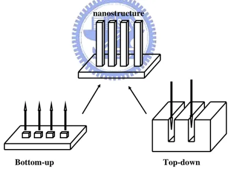
(12) Chapter 1 Introduction. 1.1 Introduction to nanotechnologies for one-dimensional nanostructures Nanostructures - structures that have at least one dimension between 1 and 100 nm - have received much interest due to their peculiar and fascinating properties and applications superior to their bulk counterparts.1-3 The ability to fabricate such a nanostructure is essential to much of modern science and technology.. There are two. major aspects: “top-down” and “bottom-up” techniques as shown in Fig.1-1 to fabricate one-dimensional structures of nanometer-length scale. nanostructure. Bottom-up. Top-down. Fig. 1-1 Diagram of top-down and bottom-up.. The techniques of the top-down aspect have been developed for a long time and used in semiconductor industry such as ultraprecision machining, micro lithography, etc.. When structure scale approaches nano-size, the manufacture of nanostructure. has a lot of difficulties that have to be overcome in the top-down method, so that the. 1.
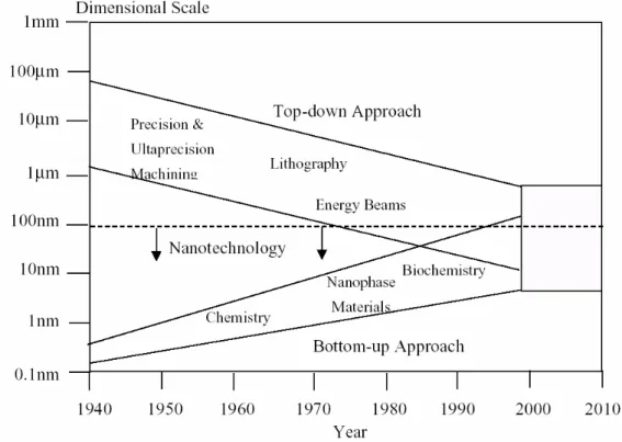
(13) bottom-up method has attracted more and more research attention on making up the nanostructure in the recent years, as shown in Fig. 1-2. Up to present, one-dimension semiconductor nanostructures such as nanowires, nanotubes, nanobelts, nanocombs, nanocantilevers and nanosprings4-9 have been fabricated by the bottom-up methods such as chemical vapor deposition (CVD), laser ablation, vapor phase evaporation, and solution and template based methods.10-14. Fig. 1-2.The development tendency of minimum process. Different types of one dimensional semiconductor nanostructures have been developed and applied to various nanoscale devices, such as nanotransistor, nano-logic gate, nanophotonics , nano-laser source, nano-grating and nanoscale photonics integration (Fig. 1-3 (a)~(g) ). 2.
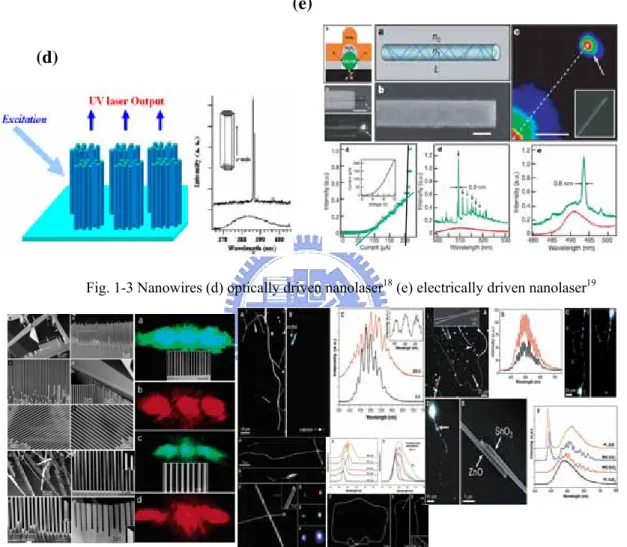
(14) (a). (b). (c). Fig. 1-3 (a) Coaxially-gated nanowire transistors15 (b) Nano-logicgate16 (c) Nanophotonics17. (e) (d). Fig. 1-3 Nanowires (d) optically driven nanolaser18 (e) electrically driven nanolaser19. Fig. 1-3 (f) Nanograting 20 (g) Nanoscale photonics integration21. 1.2 Properties of ZnO and ZnO-based compounds ZnO has attracted considerable scientific and technological attention due to its wide direct bandgap of 3.37 eV that is suitable for blue and ultraviolet (UV) optoelectronic applications.. In this regard, exciton binding energy of ZnO is 60 meV,. 3.
(15) which is significantly larger than that of ZnSe (22 meV) and GaN (25 meV). Therefore, exciton stability of ZnO provides opportunities for making highly efficient optoelectronic devices at room temperature. Moreover, based on high-quality ZnO ternary compounds formed with effectively doped impurities, the ZnO-based compounds can be systematically bandgap engineered from 3 eV (Zn0.93Cd0.07O) to 4 eV (Zn0.67Mg0.33O) at room temperature22, and the p-type conductivity has been formed with nitrogen, phosphorous, or arsenic doped ZnO.23-25. 1.3 Review of ZnO nanostructures in photonic applications ZnO-based one-dimensional nanoscale materials, as important functional oxide nanostructures, have received increasing attention over the past few years due to their potential applications in nanoscale photonic devices.. Under different morphologies. of ZnO nanostructures, nanowires, nanoribbons, and nanocombs [as shown in Fig. 1-4(a)~(c)] have been fabricated for various potential applications. For photonic applications, short-wavelength light emitting devices (LED)26, room-temperature ultraviolet nanolasers18,27 and solar cells28 are a few example.. Up to present, these. different morphologies of ZnO have been grown on sapphire and silicon substrate by simple vapor transport deposition, laser-MBE and MOCVD process.. The formation. mechanism of ZnO on the nano-length scale had also investigated29,30.. The more. complicated ZnO-based nanostructures were fabricated. For example, the inverse ZnO structure, the periodic ZnO nanowire array and the ZnO/ZnMgO nanorod heterostructures were made for studying the photonic properties, as shown in Fig. 1-4(d)~(f).. 4.
(16) (a). (b). (e). (f). (c). (g). Fig.1-4 (a) ZnO nanowire,18 (b) ZnO nanoribbon,27 (c) ZnO nanocomb,8 (d) periodic ZnO nanowire array,31 (f) ZnO inverse opal nanostructure,32 and (g) multiple quantum well (ZnO/ZnMgO) nanorod33. 1.4 Motivation The ZnO material has a very high UV emission efficiency at room temperature (free exciton binding energy is 60 meV).. The UV lasing was observed in ZnO. nanowires and lasing action was confirmed with the endfaces of the nanowire serve as the Fabry-Perot optical cavity.. Therefore, we plan to employ a thermal vapor. deposition process to grow ZnO nanostructures without catalyst in order to investigate the relationship between their morphology and the optical properties. Most of the reported researches on synthesis of randomly oriented ZnO saw-like nanostructures on Si substrate were emphasized on their growth mechanisms8,34.. In view of the. morphology of ZnO nanosaws, instead we will emphasize on investigation of optical properties of ZnO nanosaws.. Moreover, heterostructure is one of the key structures. for creating various electronic and optical devices using compound semiconductors. 5.
(17) The ZnxMg1-xO system has optical characteristics of wide bandgap that has the wider optical bandgap with increasing Mg concentration.. Therefore, we plan to. synthesize the ZnxMg1-xO nanowires (Zn2+=0.6Å, Mg2+=0.57Å) on sapphire substrate that modulate the optical bandgap with keeping the form of nanowire.. Pulsed optical. pumping will also be used to investigate stimulated emission in both of the ZnO nanosaws and the ZnxMg1-x O nanowires.. 1.5 Organization of thesis Beside this chapter, the thesis includes other four chapters.. In chapter 2 we will. exhibit the theoretical background of the experiments such as the thermal vapor process, scanning electron microscopy (SEM), energy dispersive X-ray (EDX), transmission electron microscope (TEM), x-ray diffraction (XRD) spectrum, Raman scattering and photoluminescence (PL) spectrum systems, respectively. In chapter 3, we display the experimental details including the measurement apparatus and processes.. By means of the SEM, TEM, XRD, Raman, and PL spectrum, the. morphology, crystalline quality, and optical emission properties of ZnO nanosaws and ZnMgO nanowires will be investigated and discussed in the chapter 4. Then we made a conclusion in the final chapter.. 6.
(18) Chapter 2 Theoretical background. 2.1 Growth mechanism of one-dimensional ZnO nanostructures Most popular approach for forming 1-D nanostructures is the vapor-liquid-solid (VLS) methods35.. The VLS method was originally developed by Wagner and his. co-workers to produce micrometer-sized whisker in 1960s36. technique is re-examined by Lieber35.. Recently, this. In the VLS method, the catalyst plays a key. role on the growth of the nanowires or nanorods.. The catalyst would form an alloy. nanocluster with the reactant under the proper conditions.. The growth of the. nanowires results from the alloy nanoclusters are supersaturated in the reactant. The formation procedure of 1-D nanostructure in the VLS method is shown in Fig. 2-1, which demonstrates the formation of semiconductor nanowire using metal catalyst. The reactant metal vapor which could be generated by the thermal evaporation is condensed to the catalyst metal to form a liquid alloy nanocluster as the temperature is low.. Nanowires grown after the liquid metal alloys become supersaturated and. continue as long as the metal nanoclusters remain in a liquid state. Growth of nanowires will be terminated as the temperature reduces to the point that the metal nanoclusters solidify.. Therefore, a strong evidence of the VLS mechanism is to. observe catalytic metal at the ends of the nanowires as that observed on the formation of Ge nanowires in the report by P. Yang et al.,37 as shown in Fig. 2-2.. Based on the. VLS growth mechanism, ZnO nanowires had been successfully grown on silicon substrates also by P. Yang et al. 30. 7.
(19) vapor metal catalysts. nanowire. alloy liquid. Fig. 2-1 VLS method. g Alloying. I. II. Nucleation. III Growth. Fig. 2-2 In situ TEM images recorded during the process of nanowire growth. (a) Au nanoclusters in solid state at 500 C; (b) Alloying is initiated at 800 oC, at this stage Au exists mostly in solid state; (c) liquid Au/Ge alloy; (d) the nucleation of a Ge nanocrystal on the alloy surface; (e) Ge nanocrystal elongates with further Ge condensation; (f) eventually forms a wire; and (g) Au-Ge binary phase diagram.. 2.2 Scanning Electron Microscope (SEM) and Energy Dispersive X-rays Spectroscopy (EDS) The principle of SEM used for examining a solid specimen in the emissive mode is closely comparable to that of a closed circuit TV system shown in Fig. 2-3.. In the. TV camera, light emitted from an object forms an image on a special screen, and the signal from the screen depends on the intensity of image at the point being scanned. The signal is used to modulate the brightness of a cathode ray tube (CRT) display, and. 8.
(20) the original image is faithfully reproduced if (a) the camera and display raster are geometrically similar and exactly in time and (b) the time for signal collection and processing is short compared with the time for the scan moving from one picture point to the next. In the SEM the object itself is scanned with the electron beam and the electrons emitted from the surface are collected and amplified to form the video signal.. The. emission varies from point to point on the specimen surface, and so an image is obtained. Many different specimen properties cause variations in electron emission, thus, although information might be obtained about all these properties, the images need interpreting with care.. The resolving power of the instrument can not be. smaller than the diameter of the electron probe scanning across the specimen surface, and a small probe is obtained by the demagnification of the image of an electron source by means of electron lenses. The lenses are probe forming rather than image forming, and the magnification of the SEM image is determined by the ratio of the sizes of raster scanned on the specimen surface and on the display screen. For example, if the image on the CRT screen is 100 mm across, magnifications of 100X and 10000X are obtained by scanning areas on the specimen surface 1mm and 10µm across, respectively.. One consequence is that high magnifications are. easy to obtain with the SEM, while very low magnifications are difficult.. This is. because large angle deflections are required which imply wide bore scan coils and other problem parts, and it is more difficult to maintain scan linearity, spot focus and efficient electron collection at the extremes of the scan.. 9.
(21) (b). (a). Fig.2-3 (a) Closed circuit TV and (b) scanning electron microscope. Energy Dispersive X-rays Spectroscopy (EDS) is a standard procedure for identifying and quantifying elemental composition of sample areas as small as a few square micrometers.. The characteristic X-rays are produced when a material is. bombarded with electrons in an electron beam instrument, such as a scanning electron microscope (SEM).. Detection of these x-rays can be accomplished by an energy. dispersive spectrometer, which is a solid state device that discriminates among X-ray energies, as shown in Fig. 2-4.. Fig.2-4 Schematic diagram for Energy Dispersive X-rays Spectroscopy. 2.3 Transmission electron microscopy (TEM) TEM is an analytical imaging technique whereby a beam of electrons are focused onto a specimen causing an enlarged version to appear on a fluorescent screen or layer of photographic film.. Like all matter, electrons have both wave and particle. properties, and their wave-like properties mean that a beam of electrons can in some 10.
(22) circumstances be made to behave like a beam of radiation.. The wavelength is. dependent on their energy, and so can be tuned by adjustment of accelerating fields, and can be much smaller than that of light, yet they can still interact with the sample due to their electrical charges.. Electrons are generated by a process known as. thermionic discharge in the same manner as that at the cathode in a cathode ray tube; they are then accelerated by an electric field and focused by electrical and magnetic fields on to the sample.. Details of a sample can be enhanced in light microscopy by. the use of stains; similarly with electron microscopy, compounds of heavy metals such as lead or uranium can be used to selectively deposit heavy atoms in the sample and enhance structural detail, the dense electron clouds of the heavy atoms interacting strongly with the electron beam.. The electrons can be detected using a photographic. film, or fluorescent screen among other technologies. 38 Fig. 2-5 illustrates the principal results of electron scattering by a sample and, as a result, the principal sources of information that can be obtained. The operating modes are as follows: TEM, SEM, scanning transmission electron microscopy (STEM), and microanalysis (by X-ray and/or energy loss analysis or Auger analysis of surfaces).. Fig. 2-5 Schematic showing electrons and electromagnetic waves emitted from a specimen as a result of elastic and inelastic scattering of the incident electron waves.. 11.
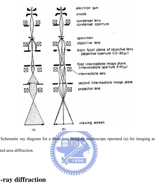
(23) In the TEM mode, which is the most often encountered, the microscope is operated as in Fig. 2-6 (a) to form images in bright field, dark field, or lattice image phase contrast mode and in Fig. 2-6 (b) to form diffraction patterns by using selected area apertures and focusing the intermediate lens on the diffraction pattern formed in the back focal plane of the objective lens.. Simple ray diagrams to illustrate these. two modes are shown in Fig. 2-6. In the following sections the specially important methods of dark field imaging, selected area diffraction, and lattice imaging are discussed. As the collimated beam of electrons passes through the crystalline specimen, it is scattered according to Bragg’s law. The beams that are scattered at small angles to the transmitted beam are focused by the objective lens to form a diffraction pattern at its back focal plane (Fig. 2-6).. When the intermediate and projector lens system is. properly focused, a magnified image of the back focal plane of the objective lens will be projected on the viewing screen. An intermediate aperture may be inserted at the first intermediate image plane to limit the field from which the diffracted information is obtained.. The intermediate selected area diffraction (SAD) aperture makes it. possible to obtain diffraction patterns from small portions of the specimen.. This. technique is very useful, since a direct correlation can be readily made between the morphological and crystallographic information of very small areas.. It is also. necessary for establishing the diffracting and contrast conditions in the image.. The. technique is of particular importance when more than one phase is present in the specimen. 39. 12.
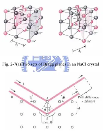
(24) Fig. 2-6 Schematic ray diagram for a three-lens imaging microscope operated (a) for imaging and (b) for selected area diffraction.. 2.4 X-ray diffraction A crystal consists of a regular array of atoms, each of which can scatter electromagnetic waves. A monochromatic beam of X-rays that falls upon a crystal will be scattered in all directions inside it.. However, owing to the regular. arrangement of the atoms, in certain directions the scattered waves will constructively interfere with one another while in others they will destructively interfere. The atoms in a crystal may be thought of as defining families of parallel planes, as in Fig. 2-7(a), with each family having a characteristic separation between its component planes.. This analysis was suggested in 1913 by W. L. Bragg.. The conditions that. must be fulfilled for radiation scattered by crystal atoms to undergo constructive interference may be obtained from a diagram as in Fig. 2-7(b). 13. A beam containing.
(25) X-ray of wavelength λ is incident upon a crystal at an angle θ with a family of Bragg planes whose spacing is d.. The beam goes past atom A in the first plane and atom B. in the next, and each of them scatters part of the beam in random directions. Constructive interference takes place only between those scattered rays that are parallel and whose paths differ by exactly λ, 2λ, 3λ, and so on.. That is, the path. difference must be nλ, where n is an integer. The only rays scattered by A and B for which this is true are those labeled I and II in Fig. 2-7(b).. Fig. 2-7(a) Two sets of Bragg planes in an NaCl crystal. Fig. 2-7(b) X-ray scattering from a cubic crystal. The first condition on I and II is that their common scattering angle must be equal to the angle of incidence θ of the original beam. The second condition is that 2d sin θ = nλ ,. n = 1,2,3,.... (2-1). since ray II must travel the distance 2d sin θ farther than ray I. The integer n is the order of the scattered beam.40. Then considering a hexagonal unit cell in Fig. 2-8 14.
(26) which is characterized by lattice parameters a and c. The equation of plane spacing for the hexagonal structure is 41 1 4 ⎛ h 2 + hk + k 2 = ⎜ d 2 3 ⎜⎝ a2. ⎞ l2 ⎟⎟ + 2 . ⎠ c. (2-2). Combining Bragg’s law (λ= 2d sin θ ) with (2-2) yields: 1 4 ⎛ h 2 + hk + k 2 ⎜ = d 2 3 ⎜⎝ a2. ⎞ l 2 4 sin 2 θ ⎟⎟ + 2 = . λ2 ⎠ c. (2-3). Rearranging (2-3) gives sin 2 θ =. λ2 4 ⎛ h 2 + hk + k 2 ⎞ { ⎜ 4 3 ⎜⎝. a2. l2 ⎟⎟ + 2 }, ⎠ c. (2-4). Thus the lattice parameters can be estimated from eq. 2-4.. Fig. 2-8 The hexagonal unit cell. 2.5 Raman scattering When light passes through a medium, it is reflected, transmitted, absorbed, elastic scattered, or inelastic scattered. Raman scattering is an inelastic scattering process.. When the light encounters the medium, it interacts inelastically with. phonons and produces an outgoing photon whose frequency is relatively shifted by an amount of energy corresponding to phonon energy from that of the incoming light.. 15.
(27) The scattered outgoing photons are called the Raman-scattered photons. If the light of frequency ν 0 is scattered by some media, the spectrum of the scattered light contains. a. strong. line. of. frequency. ν0. and. much. frequencies ν 0 − ∆ν 1 , ν 0 − ∆ν 2 ,………, ν 0 + ∆ν 2 , ν 0 + ∆ν 1 , etc.. weaker. lines. of. Those lines on the. low frequency side of the excitation line (i.e.ν 0 − ∆ν i , I = 1, 2,……) are always matched by lines on the high frequency side (i.e.ν 0 + ∆ν i , I = 1, 2,……), but the latter are much weaker when the scattering medium is at room temperature.. Raman. scattering is inherently a weak process, but laser provides enough intensity that the spectra can be routinely measured. In analogy with terms used in the discussion of fluorescence spectra, lines on the low frequency side of the excitation line are known as the Stokes lines and those on the high frequency side as the anti-Stokes lines. The incident photon loses its energy by producing a phonon (Stokes shifted), or gain energy and momentum by absorbing a phonon (anti-stokes shifted), according to the energy and momentum conservation rules: hν s = hν i ± hΩ qs = qi ± K. ,. where ν i and ν s are the incoming and scattered photon frequencies, qi and qs are the incoming and scattered photon wavevectors, and Ω and K are the phonon frequency and wavevector, respectively. All of the Raman mode frequencies, intensities, line-shapes, and line-widths, as well as polarizations can be used to characterize the lattices and impurities. The intensity gives information on crystallinity.. The line-width increases when a. material is damaged or disordered, because damage or disorder occurs in a material will increase phonon damping rate or relax the rules for momentum conservation in Raman process.. All these capabilities can be used as a judgment for layered. microstructures as well as bulk materials, subject only to the limitation that the. 16.
(28) penetration depth of the excitation radiation range from a few hundred nanometers to few micrometers. The E2 mode of the wurtzite ZnO crystal would shift to a higher frequency under the biaxial compressive stress within the c-axis oriented ZnO by the equation:. ∆ω (cm −1 ) = 4.4σ (GPa) ,. (2-5). where ∆ω is the frequency shift, and σ is the stress in the biaxial direction of lattice.. 2.6 Photoluminescence Characterization Photoluminescence (PL) is a very useful and powerful optical tool in the semiconductor industry, with its sensitivity to find the emission mechanism and band structure of semiconductors. From PL spectrum the defect or impurity can also be found in the compound semiconductors, which affect material quality and device performance. A given impurity produces a set of characteristic spectral features. The fingerprint identifies the impurity type, and often several different impurities can be seen in a single PL spectrum. In addition, the full width of half magnitude of each PL peak is an indication of sample’s quality, although such analysis has not yet become highly quantitative.42 PL is the optical radiation emitted by a physical system (in excess the thermal equilibrium blackbody radiation) resulting from excitation to a nonequilibrium state by illuminating with light. Three processes can be distinguished: (i) creation of electron-hole pairs by absorption of the excited light, (ii) radiative recombination of electron-hole pairs, and (iii) escape of the recombination radiation from the sample. Since the excited light is absorbed in creating electron-pair pairs, the greatest excitation of the sample is near the surface; the resulting carrier distribution is both. 17.
(29) inhomogeneous and nonequilibrium.. In attempting to regain homogeneity and. equilibrium, the excess carriers will diffuse away from the surface while being depleted by both radiative and nonradiative recombination processes. Most of the excitation of the crystal is thereby restricted to a region within a diffusion length (or absorption length) of the illuminated surface. Consequently, the vast majority of PL experiments are arranged to examine the light emitted from the irradiated side of the samples. This is often called front surface PL.. 2.6.1. Fundamental Transitions Since emission requires that the system be in a nonequilibrium condition, and some means of excitation is acting on the semiconductor to produce hole-electron pairs. We consider the fundamental transitions, those occurring at or near the band edges. 1. Free excitons A free hole and a free electron as a pair of opposite charges experience a coulomb attraction. Hence the electron can orbit about the hole as a hydrogen-like atom. If the material is sufficiently pure, the electrons and holes pair into excitons which then recombine, emitting a narrow spectral line.. In a direct-gap. semiconductor, where momentum is conserved in a simple radiative transition, the energy of the emitted photon is simply hν=Eg – Ex, where Eg and Ex are the band gap and the exciton binding energy. 2. Bound excitons Similar to the way that free carriers can be bound to (point-) defects, it is found that excitons can also be bound to defects. A free hole can combine with a neutral donor to form a positively charged excitonic ion. In this case, the electron bound to 18.
(30) the donor still travels in a wide orbit about the donor. The associated hole moves in the electrostatic field of the “fixed” dipole, determined by the instantaneous position of the electron, then also travels about this donor; for this reason, this complex is called a “bound exciton”. An electron associated with a neutral acceptor is also a bound exciton. The binding energy of an exciton to a neutral donor (acceptor) is usually much smaller than the binding energy of an electron (hole) to the donor (acceptor).. 3. Donor-Acceptor Pairs Donors and acceptors can form pairs and act as stationary molecules imbedded in the host crystal. The coulomb interaction between a donor and an acceptor results in a lowering of their binding energies. In the donor-acceptor pair case it is convenient to consider only the separation between the donor and the acceptor level: Epair =Eg – (ED +EA) +. q2. ε. r. ,. (2-6). where r is the donor-acceptor pair separation, ED and EA are the respective ionization energies of the donor and the acceptor as isolated impurities.. 4.. Deep transitions By deep transition we shall mean either the transition of an electron from the. conduction band to an acceptor state or a transition from a donor to the valence band in Fig. 2-9. Such transition emits a photon hν=Eg – Ei for direct transition and hν=Eg – Ei -Ep if the transition is indirect and involves a phonon of energy Ep. Hence the deep transitions can be distinguished as (1) conduction-band-to-acceptor transition which produces an emission peak at hν = Eg – EA, and (2) donor-to-valence-band transition which produces emission peak at the higher photon. 19.
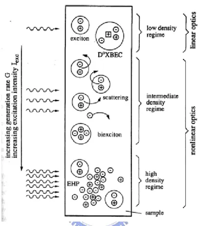
(31) energy hν=Eg – ED.. C D. A V Fig. 2-9 Radiative transition between a band and an impurity state.. 5. Transitions to deep levels Some impurities have large ionization energies; therefore, they form deep levels in the energy gap. Raditive transitions between these states and the band edges emit at hν=Eg – Ei.43. 2.6.2 Influence of high excited light intensity44 The PL conditions as mentioned above are excited by low excitation light intensity. At low excitation light intensity (low density regime in Fig. 2-10), the PL properties are determined by single electron-hole pairs, either in the exciton states or in the continuum. Higher excitation intensity (intermediate density regime in Fig. 2-10) makes more excitons; such condition would lead to the exciton inelastic scattering processes and form the biexciton. The scattering processes may lead to a collision-broadening of the exciton resonances and to the appearance of new luminescence bands, to an excitation-induced increase of absorption, to bleaching or to optical amplification, i.e., to gain or negative absorption depending on the excitation conditions. If we pump the sample even harder, we leave the intermediate and arrive at the high density regime in Fig. 2-6, where the excitons lose their identity. 20.
(32) as individual quasiparticles and where a new collective phase is formed which is known as the electron-hole plasma (EHP).. Fig. 2-10 The general scenario for many-particle effects in semiconductors44. 1.. Scattering Processes In the inelastic scattering processes, an exciton is scattered into a higher excited. state, while another is scattered on the photon-like part of the polariton dispersion and leaves the sample with high probability as a luminescence photon, when this photon-like particle hits the surface of the sample.. This process is shown. schematically in Fig. 2-11 and the photons emit in such a process have energies En given by Ref. 28. 1⎞ 3 ⎛ En = Eex − Ebex ⎜1 − 2 ⎟ − kT , ⎝ n ⎠ 2. (2-7). where n = 2, 3, 4,…, Ebex =60meV is the binding energy of the free exciton of ZnO, 21.
(33) and kT is the thermal energy.. The resulting emission bands are usually called. P-bands with an index given by n.. energy continuum. nB= ∞ 2. Eg. 1 P2 Eexciton. P∞. Wave vector. Fig.2-11 Schematic representation of the inelastic exciton-exciton scattering processes.44. 2. Electron-Hole Plasma In this high density regime, the density of electron-hole pairs np is at least in parts of the excited volume so high that their average distance is comparable to or smaller than their Bohr radius, i.e., we reach a “critical density” n cp in an EHP, given to a first approximation by aB3 n cp ≈ 1 .. We can no longer say that a certain electron is. bound to a certain hole; instead, we have the new collective EHP phase.. The. transition to an EHP is connected with very strong changes of the electronic excitations and the optical properties of semiconductors.. 22.
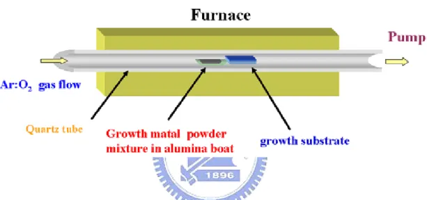
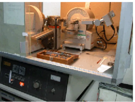
(34) Chapter 3 Experiment Details. 3.1 Sample Preparation 3.1.1 Substrate preparation Silicon (100) wafer and a-plane sapphire were used as the substrate for the growth of ZnO-based nanostructures. Before the surface treatment, the substrates were cut into an area of 10╳5 mm2 for the nanostructures growth. Then these substrates were cleaned by using the following steps: (1) Rinsed in D. I. water by a supersonic oscillator in 20 min. (2) Rinsed in ACE (Acetone) solution by a supersonic oscillator in 20 min. (3) Rinsed in D.I water by a supersonic oscillator in 20 min. (4) Dried with N2 gas. (5) Baked at 200°C on hot plate. After the surface treatment, the substrates were placed in an alumina boat filled with the growth metal and ready to grow ZnO-based nanostructures.. 3.1.2 Growth of ZnO and ZnMgO nanostructures The substrate was placed on the alumina boat filled with pure Zn powder (99.9999 %) or mixture of Zn and Mg (99.6 %) powders. The vertical distance between the metal source and the sample was about 3~5 mm. Then the alumina boat which carried the substrate was inserted into a quartz tube. This quartz tube was placed inside a furnace, with the center of the alumina boat positioned at the center of the furnace and the substrates placed downstream of growth metal powder (Fig. 3-1). The quartz tube was evacuated to a pressure below 2╳10-2 torr using mechanical pump. After the high-purity argon gas was infused into the system with 23.
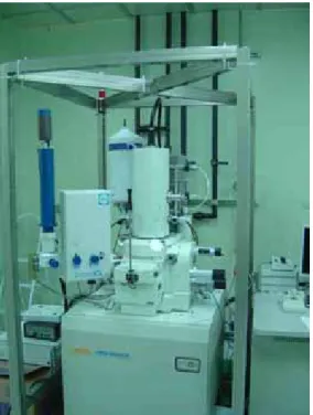
(35) a flow rate of 200 sccm and pressure controlled at 50 sccm. The temperature of the furnace was increased to 5700C~7000C at a rate of 20-300C min-1 and then kept at fixed temperature for 30~60 min under an O2 flow at about 2 sccm.. After the. furnace was cooled to the room temperature, dark gray-white material was obtained on the surface of the substrates.. Fig. 3-1 Thermal vapor transport system. 3.2 Scanning Electron Microscope (SEM) system The morphology of ZnO-based nanostructures were observed by the Field Emission Gun Scanning Electron Microscopy (FEG-SEM) [JEOL JSM-6500F]. The accelerated voltage is 0.5-30kV and the magnification is 20-300k times, as shown in Fig. 3-2.. 24.
(36) Fig. 3-2 SEM system. 3.3 Transmission electron microscope (TEM) system The detailed structure of ZnO-based nanostructures can be found by TEM. The TEM images were taken by JEOL JEM-2000FX transmission electron microscope (TEM) operated at 200 keV. The prepared nanowires were firstly suspended in alcohol by supersonic jolt and then the suspension was moved to the copper grid for observation, as shown in Fig. 3-3.. 25.
(37) Fig. 3-3 TEM system. 3.4 X-ray diffraction After growing the nanostructures, the crystalline structures of the as-grown ZnO nanowires were analyzed by using Philips PW1700 X-ray diffractometer (XRD) with Cu Ka radiation (λ=1.5405 Å). The maximum voltage of the system is 40 kV with a maximum current 40 mA. The scanning step is 0.020 and scanning rate is 40 /min, as shown in Fig. 3-4.. Fig. 3-4 XRD system. 26.
(38) 3.5 Raman system The optical characterization was analyzed with Raman measurement. A 5mW Ar-ion laser with an incident wavelength of 488 nm was used as the excitation source for the Raman spectroscopy. The scattered light was collected using backscattering geometry and detected by the SPEX 1877 triplemate equipped with liquid nitrogen cooled CCD. Measurements were carried out at room temperature, as shown in Fig. 3-5.. Fig. 3-5 Raman system. 3.6 Photoluminescence (PL) system For cw PL measurement, we used a He–Cd laser (325 nm) [Kimmon IK5552R-F] as the excitation source; for pulsed pumping, we used the third harmonic of Nd:YVO4 laser (355 nm) [JDS uniphase CDRH Power Chip Nanolaser] with pulse width of ~500 ps and repetition rate of 1KHz.. The emission light was dispersed by a. TRIAX-320 spectrometer and detected by a UV-sensitive photomultiplier tube. As shown in Fig. 3-6 and Fig. 3-7.. 27.
(39) He-Cd laser (325 nm). M1. M3 (Focus lens). Triax 320. M4 (Focus lens) Sample holder. M2. Fig. 3-6 PL system. Pulse laser (355 nm) M5 (Focus lens). Sample holder. Collecting fiber. Triax 320. Fig. 3-7 High power pumping PL system. 28.
(40) Chapter 4 Results and Discussion. 4.1 Structural and optical properties of saw-like ZnO nanostructures 4.1.1 Growth of ZnO nanosaws on Si substrate Synthesis of ZnO nanostructure was achieved in a simple vapor transport process45. First, a very thin layer of Au was deposited on a (100)-silicon substrate. A mixture of pure zinc powder (99.9999%) and Mg3N2 powder (99.6%) with a weight ratio of 10:1 was placed in a ceramic boat as the starting materials. The boat was positioned in the center of the quartz furnace tube and the substrate was placed 5 cm downstream from the mixed powder.. After the high-purity argon gas was infused. into the system with a flow rate of 200 sccm, the furnace temperature was increased to 700°C and kept at this temperature for 60 min under an O2 flow at about 2 sccm. After the reaction is complete, the system was cooled to the ambient temperature and a gray-white colored product was found deposited on the substrate.. 4.1.2 Structural properties and growth mechanism of ZnO nanosaws As shown in Figure 4-1(a), the typical SEM micrograph clearly reveals that a large quantity of one dimension nanostructure was formed on the Si substrate. A high magnification SEM image is shown in Fig. 4-1(b)-(c). The saw-shape nanostructure, with one side flat and the other side with teeth, is the most dominant morphology. Typical length of nanosaws exceeds several tens of µm with sharp teeth in a saw having length of about 1-5 µm and diameter ranging about 100 nm. Figure 4-1(d) shows EDX spectrum, revealing the nanosaws contain Zn and O. 29.
(41) elements, with no other detectable elements.. (d). Counts (a.u.). Zn. O. 0. 1. 2. 3. 4. 5. Energy (keV). Figure 4-1 (a) The SEM image of the ZnO nanosaws, (b)-(c) magnified SEM image of the ZnO nanosaws, and (d) The EDX of the ZnO nanosaws.. Figure 4-2 shows the XRD pattern of the sample. All diffraction peaks and their relative intensities coincide with the JCPDS card no. 36-1451.. Therefore, the. products are the hexagonal ZnO phase with random orientation and distribution. The lattice constants calculated according to the following equations to be a=3.246 Å and c=5.2 Å,: 30.
(42) a=. c=. λ 2 sin θ. λ 2 sin θ. 4 2 l2 (h + hk + k 2 ) + 3 (c / a ) 2. (4-1). 4 (h 2 + hk + k 2 ) + l 2 , 2 3(c / a ). (4-2). where h, k, l are Miller exponents, and λ=1.54056Å and θ are X-ray wavelength and. 30. 35. 40. 45. 50. 55. 60. (103). Si (111). (102). (110). (002). (100). Intensity (a.u.). (101). Bragg angle, respectively.. 65. 2θ (degrees). Figure 4-2 The XRD pattern of the ZnO nanosaws. Figure 4-3(a) shows the TEM image of the sharp teeth of the nanosaws. The width of the teeth is nearly 50 nm.. The double image of the nanowires is due to. overlapping the one on top of another. The selected-area electron diffraction (SAED) pattern is displayed in Fig. 4-3(b).. The appearance of diffraction spot (0002). confirms that teeth of a nanosaw growth along the c-axis direction (along [0001]). The discrete diffraction spots indicate that the ZnO nanosaws is single crystalline revealing that the nanosaw is hexagonal wurtzite single-crystalline ZnO. This result 31.
(43) is known that the growth direction of several ZnO nanostructures have been identified in the literature7~8,30,46~47. Figure 4-3(c) shows an HRTEM image taken from the side of teeth of a nanosaw, which indicates the perfect lattice structure of the nanosaw and the d-spacing between any two neighboring lattice fringes is 0.52 nm and 0.28 nm which match that of [0001] direction and [ 01 1 0 ] direction of the wurtzite ZnO, respectively. Schematic models on the geometrical shape and the corresponding crystallographic facets are given in Fig. 4-3(d). The growth mechanism of the nanosaws is likely the self-catalyst process, which originates from Zn or ZnOx clusters48. The possible growth procedure for typical ZnO nanosaw is as follow.. The Zn powder turns into Zn vapor during the. evaporation duration and forms Zn or ZnOx liquid droplets as the nucleation site of the ZnO nanostructures. Then the solid ZnO particle separates from the droplets, and ZnO nanoribbon formed first. As the reaction process proceeded with Zn vapor turned into Zn or ZnOx liquid droplets, and deposited on the new nucleation sites on the ZnO nanoribbon. Finally, it is known to us that [0001] is the fastest growth direction in the only grew along one side of ZnO nanostructures, including the comb-structure7-8,47-48 and it corresponds to the formation of ZnO nanosaws.. (d). Figure4-3 (a)TEM image of the ZnO nanosaws. (b)SAED of the ZnO branches.(c)HRTEM image of the branches of the ZnO nanosaws.(d) Schematic model of the nanosaw 32.
(44) 4.1.3. Optical properties of ZnO nanosaws The typical Raman spectrum of the ZnO nanosaws is shown in Fig. 4-4.. The Raman peaks at 378 and 436 cm-1 originate from vibration modes of A1(TO) (transverse optical, TO) and E2(high), respectively. The higher frequency of the Raman spectrum was observed that the longitudinal optical (LO) phonon modes are two polar symmetric modes with A1(LO) and E1(LO). The peaks of A1(LO) and E1(LO) were fitted to the spectrum in the insert of Fig. 4-4, which are at 574 and 583 cm-1, respectively. The result is consistent with the values of ZnO powder (or bulk crystal)49. The E2(high) mode corresponds to band characteristic of wurtzite phase. The appearance of the E1(LO) peak has been attributed to the formation of oxygen vacancy and interstitial zinc atom. The PL spectra of ZnO nanosaws measured at room temperature are shown in Fig. 4-5. Under cw laser excitation, the spectrum shows a strong UV emission peak having photon energy about 3.22 eV with FWHM~ 150 meV (Wavelength=385 nm, FWHM~ 18 nm) and weak green band having a broad feature in the range of 1.9 eV~2.8 eV (wavelength=440 nm~650nm).. This sharp UV emission peak is. attributed to the near band edge emission45,50. As comparison with ZnO bulk crystal (photon energy of free exciton is 3.28 eV), slight shift of the emission peak toward the lower energy in ZnO nanosaws results from a mixture of free exciton and other impurity-related transitions50 or the effect of the thermal energy caused by laser heating. The emission of broad peak is the deep-level emission, which is attributed to the oxygen vacancy. The strong UV emission and weak green emission in PL spectra indicate that the ZnO nanosaws have a good crystal quality with few oxygen vacancies.. 33.
(45) A1(TO). Intensity(a.u.). Intensity(a.u.). E2(high). LO phonon mode peak E1(LO). A1(LO). 550 560 570 580 590 600 Raman shift (cm-1). 400. 450. 500. 550 Raman shift (cm-1). 600. PL intensity(a.u.). Fig. 4-4 The Raman spectra of the ZnO nanosaws. 2.0. 2.2. 2.4 2.6 2.8 3.0 Photon Energy(eV). 3.2. Fig. 4-5 The PL spectra of the ZnO nanosaws. 34. 3.4. 650.
(46) 4.1.4 Random lasing in ZnO nanosaws at room temperature In Fig. 4-6(a) shows excitation intensity dependence of emission spectra under pulse laser excitation.. Under low excitation intensity, the spectrum is. composed of a single broad peak of amplified spontaneous emission at 3.2 eV with FWHM~115 meV.. As increasing the excitation intensity, the emission peak. becomes narrower due to the preferential amplification at wavelength close to the maximum of the gain spectrum.. When the excitation intensity exceeded a threshold,. Ith=0.96 MW/cm2 in Fig. 4-6(b), several narrow peaks emerged in the emission spectra at around 3.18 eV. The linewidth of these peaks was less than 4 meV. When the pumping intensity increased further, more sharp peaks appeared. The spectrally emission intensity as a function of the excitation intensity is shown in Fig. 4-6(b). Above a certain pump threshold, the intensity of the multiple sharp peaks increases much more rapidly with the pump intensity. These results indicate a clear evidence of lasing action. Note that the position of PL emission peak redshifts with increasing pumping intensity, which is caused by the bandgap renormalization.51. 35.
(47) PL intensity(a.u.). (a). 3.0. 3.1. 3.2 Photon Energy (eV). 3.3. Intergrated intensity(a.u.). (b). Increasing pumping density. Ith=0.96 MW/cm2. 0.0. 0.5 1.0 1.5 2.0 Excitation density(MW/cm2). 2.5. Fig. 4-6 (a) The emission intensity of ZnO nanosaw versus the pumping intensity. (b) The threshold behavior of the emission intensity with increasing excitation density... 36.
(48) In general, the lasing action in ZnO nanostructures has two kind of lasing mechanism. from. the. The first type of lasing with the Fabry-Perot (FP) optical cavity arises structure. of. individual. nanostructures,. such. as. nanowire. and. nanoribbon18,27,52. These single-crystal nanostructure of ZnO is a gain medium by itself, which is provided by a natural optical cavity formed between the two-end facets and natural optical waveguide so that the lasing action occur in nanostructures can be observed clearly. Another lasing mechanism is called “random lasing”, that the emission light is strongly scattered in gain media, and a close-loop path can be formed through multiple scattering. These loop could serve as ring cavity for light51,53-57. Following the two possible lasing behavior in morphology of ZnO nanosaws (see Fig. 4-1) and optical pumping PL spectra (Fig. 4-6(a)), and canvassing the details further. The ZnO nanosaws show feature of resonant modes. The longitudinal mode spacing of the lasing modes can be determined by the equation, Δλ=λ2/(2nL), where L is the cavity length of the laser, n is the refractive index of ZnO (n=2.45), and λ is the resonant wavelength ~390 nm (photon energy = 3.18 eV). For a mode spacing between the closest longitudinal modes is about 0.65 nm, the cavity length is expected to be ~50μm. In spite of the ZnO nanosaw with length of about 50μm might exist, the lasing action from FP mode is less likely to occur in ZnO nanosaws. The natural PF cavity formed in ZnO nanostructure needs both good crystalline and small internal loss52,55. The morphology of ZnO nanosaw is so rough that strong light scattering occurs at the interfaces of nanosaw. Therefore; it is much more probable that the emitted light is scattered and feedback as a resonant cavity among the ZnO nanosaws. As a result of light scattering by the randomly distributed ZnO nanosaws, we can attribute the lasing behavior as random lasing action among the ZnO nanosaws. Light is amplified while following a closed random path provided that it satisfies resonance condition due to coherent multiple scattering. 37. Because of the short.
(49) scattering mean free path, the emitted light is strongly scattered in ZnO nanosaws. The closed-loop paths can be formed through multiple scattering. These loops act as ring cavities, namely, the ring cavities are “self-formed” by reduplicating scattering. To verify our laser cavities are “self-formed” by strong light scattering, we measured emission spectra at different excitation areas when the excitation intensity is fixed at 1.07 MW/cm2.. As shown in Fig. 4-7(a), before the excitation area reaches a. threshold value, the scattered light has not yet gathered sufficient in a certain close loop and thus no sharp peak emerges. When the excitation area has exceeded the threshold area (Ath~1.5 x 10⁻⁴ cm2), a closed path can be formed through multiple scattering in larger excitation area and the lasing action starts.. The schematic. diagram of the formation of the closed-loop path through multiple scattering in disorder ZnO nanosaws is shown in the inset of Fig. 4-7(a). Sharp peaks with linewidth of less than 0.6 nm (5 meV) were observed provided that laser cavity can be formed for suitable excitation area. The dependence of threshold excitation area (Ath) on the excitation density is shown in Fig. 4-7(b). As the excitation density increases, the threshold of excitation area clearly decreases. It indicates that the scattered photon acquires more gain under stronger pump density before it experiences successive scattering, and thus less optical path or smaller excitation area is required for laser action to take place.. Therefore, random cavity can be formed more. effectively under higher pump density. Figure 4-8 shows the emission spectra at different observation angle θ, which is defined from the sample surface. The black curves (a) and (b) correspond to θ=75° and θ=45° and short dash lines express the auxiliary lines of emission peaks in Fig. 4-8(a). It was quite obvious that different emission spectra can be observed at different angles. This is due to formation of different laser cavities by multiple scattering and thus different gain lengths for different cavity modes. It leads to different resonant photon energy in different 38.
(50) output direction so that different lasing spectra were observed at different angles. This behavior is similar to the previous studies on lasing action in ZnO particles and nanorod56,58. Furthermore, we measured the polarization dependence of the emission when the excitation intensity is tuned about 2.4 Ith. The emission spectra of maximum of polarized emission intensity (Imax) and minimum of polarized emission intensity (Imin) for the peak at 3.17 eV are shown in Fig. 4-9(a) that correspond to the polarized angles at 40˚ and 130˚, respectively. It reveals that the lasing peaks do not always have large degree of polarization, (Imax-Imin)/(Imax+Imin) as the solid curve of Fig. 4.9(b). And the dashed curve expresses the degree of polarization for polarizer angle rotated 40˚, which corresponds to emission spectra of polarized angles at 80˚ and 170˚. Clearly, the lasing peaks have not only different degrees of polarization but also preferable polarization at different directions. The inset of Fig. 4-9(b) shows the emission intensity (Ilasing as square dots) of sharp lasing peak at photon energy of 3.17 eV and the smooth spontaneous emission (Ispon as triangles) as a function of polarization angle which can be well fet with square of the cosine function. However, the lasing emission is partially polarized and has the larger degree of polarization (~0.2) than that of spontaneous emission equal to 0.03. Hence, we conjecture polarization of random lasing may be related to the morphology of nanostructure.. According to the report by Cao et al.54 and Yu et al.,55 the. polarization of lasing emission is concerned with the orientations of ZnO film and of ZnO nanorod. Furthermore, the spontaneous emission of ZnO nanowire had been found prefer to polarize perpendicular to c-axis52 and the degree of polarization of lasing quickly increases with increasing excitation density.59. It is reasonable that. lasing emission of ZnO nanosaw possesses partial polarization. Because the teeth of a nanosaw has a great quantity grown along the c-axis and as aforementioned the 39.
(51) strong light scattering at teeth interface, the scattered light should have preferable polarization, in turn, light, which is amplified while it follows a closed-loop random path, will be partially polarized. However, individual laser cavity has individual polarization so that we observed different degrees of polarization for different lasing peaks shown in Fig. 4-9(b) is mainly due to cavities formed by different closed-loop random paths.. 40.
(52) (a ) PL intensity(a.u.). Increasing excitation area Ath=1.5x10⁻⁴ cm2. 3.0. (b). 3.1 3.2 Photon Energy (eV). 3.3. 16. -4. 2. Athx10 (cm ). 12. 8. 4. 0. 0.6. 0.7 0.8 0.9 1.0 2 Excitation Density (MW/cm ). 1.1. Figure 4-7 (a) the dependence of excitation area on emission spectra of the ZnO nanosaws at Ip = 1.1 MW/cm2, the inset is a schematic diagram showing the formation of the closed-loop path for light through multiple scattering in the sample. (b) the threshold excitation area versus excitation density.. 41.
(53) PL intensity(a.u.). Pump Emission θ. Sample. 3.10. (a). θ=75. (b). θ=45. 3.15. 3.20 3.25 Photon Energy(eV). ο. ο. 3.30. 3.35. Figure 4-8 Emission spectra of observation angles at θ=75° and θ=45° with θ being defined from the sample surface. cm2.. The excitation power density is 1.65 MW/cm2 and the excitation area is 7.1╳10-4. The inset is a schematic diagram showing the experimental configuration.. 42.
(54) (a) PL intensity (a.u.). Imax. Imin. 3.12. 3.14. 3.16 3.18 3.20 3.22 Photon Energy(eV). 3.24. 3.26. 0.8 0.6. Imax-Imin/Imax+Imin. 0.4. Ilasing,Ephoton= 3.17 eV Ispon. Cos2(θ−40). PL intensity(a.u.). Degree of polarization. (b). 0. 20. 40. 60. 80. 100 120 140 160 180. Polarization angle(deg.). 0.2 0.0. 3.12. 3.14. 3.16 3.18 3.20 3.22 Photon Energy(eV). 3.24. 3.26. Figure 4-9 (a) the maximum (Imax) and the minimum (Imin) emission spectra of ZnO nanosaws which corresponding to the polarization angles of 40o and 130o.. (b) The degree of polarization of (a) as the. solid curve and the dash curve for that relatively rotated by 40o. The inset of (b) is the degree of polarization as a function of polarization angle for lasing peak at 3.17 eV (squares) and smooth spontaneous emission (triangles).. 43.
(55) 4.2 Room-temperature optical properties of the ZnO:MgO nanowires after heat treatment. 4.2.1 Growth of ZnO:MgO nanowires on a-plane sapphire substrate Similar to synthesis of pure ZnO nanowires or nanosaws which uses pure ZnO powder (99.9999%), ZnO:MgO nanostructures can also be grown in a simple vapor transport process. In this process zinc powder (99.9999%) and Mg powder (99.6%) with Mg:Zn weight ratios of 1:19 were placed in a ceramic boat as the starting materials. A sapphire[ 11 20 ] wafer was used as substrate. The boat was positioned in the center of the quartz furnace tube and the substrate was placed 10 mm downstream from the mixed powder.. Prior to heating the furnace, the quartz tube. was purged with high-purity argon gas for 3 min twice. The system was heated to 570 °C with an Argon flow rate of 500 sccm and kept at this temperature for 60 min. After the reaction is complete, the system was cooled to the ambient temperature and a gray-white colored product was found deposited on the substrate.. 4.2.2 Structural properties and growth mechanism of ZnO:MgO nanowires Figure 4-10(a)-(b) shows the SEM images for pure well-aligned ZnO nanowire as well as ZnO:MgO nanowires. The diameter of ZnO nanowires is about 75 nm ~100 nm and the length is several micrometers. The ZnO:MgO nanostructures have diameter of about 200-500 nm and length of over 5 µm. Figure 4-10(c)-(d) show the results of the EDX measurement. In ZnO nanowires, the EDX pattern shows that mainly composed of Zn and O, whereas in ZnO:MgO nanowires, the EDX pattern 44.
數據

+7
相關文件
2A 與健康、社會 關懷、個人與社 會福祉有關的結 構性議題. (4) 家庭問題,例
Spatially resolved, time-averaged, multipoint measurements of flame emission spectra using two Cassegrain mirrors and two spectro- meters are performed and the results are used
Taiwan customer satisfaction index (TCSI) model shown in Figure 4-1, 4-2 and 4-3, developed by the National Quality Research Center of Taiwan at the Chunghua University in
而在利用 Autocloning 的方法,製作成金字塔形狀的抗反射 結構方面。分成非次波長結構和次波長結構來加以討論。在非次波長 結構時,我們使用
The effects of radius of the pulse laser and ratio of delay times on the temperature distributions were discussed in detail.A nondiemensional parameter B was defined as the ratio
本研究為了將結構物內的牆以不同單位重來做比較,在計算每棟
本研究在有機物部分,除藉由螢光光譜儀進行螢光激發發射光 譜圖(Excitation emission fluorescent matrix,
(2011) Tracking natural organic matter (NOM) in a drinking water treatment plant using fluorescence excitation–emission matrices and PARAFAC. (2009) Relating freshwater organic
