國 立 交 通 大 學
電信工程學系
博 士 論 文
具頻率相關耦合之步階阻抗諧振器的準橢圓函數
響應濾波器之合成與實現
Synthesis and Realization of Frequency-Dependent
Coupled Stepped-Impedance Resonator Filters with a
Quasi-Elliptic Function Response
研 究 生: 徐慶陸 (Ching-Luh Hsu)
指導教授: 郭仁財 博士 (Dr. Jen-Tsai Kuo)
函數響應濾波器之合成與實現
Synthesis and Realization of Frequency-Dependent
Coupled Stepped-Impedance Resonator Filters with a
Quasi-Elliptic Function Response
研究生:徐慶陸
Student: Ching-Luh Hsu
指導教授:郭仁財 博士
Advisor: Dr. Jen-Tsai Kuo
國立交通大學
電信工程學系
博士論文
A Dissertation
Submitted to Institute of Communication Engineering
College of Electrical and Computer Engineering
National Chiao Tung University
in Partial Fulfillment of the Requirements
for the Degree of Doctor of Philosophy
in
Communication Engineering
July 2008
Hsinchu, Taiwan
中華民國九十七年七月
I
數響應濾波器之合成與實現
研究生: 徐慶陸
指導教授: 郭仁財 博士
國立交通大學
電信工程學系
摘要
本論文研究具頻率相關耦合結構的濾波器合成與實現。首先探討具頻率相 關耦合特性的三元結構(Trisection),產生一對傳輸零點的機制。具有此類型零 點的濾波器一般稱為準橢圓濾波器。僅使用頻率無關耦合特性的三元結構,通 常只能產生一個傳輸零點。本文所提出的新型三元結構能產生一對零點。濾波 器合成的演算過程中,頻率相關耦合結構的電路模型是將複數頻率變數 s 乘以 固定導納轉換器(J-inverter)。研究發現分接線(Tapped-line)結構的輸入輸出會 產生更多零點。文中將呈現具四個零點的三階電路以及具五個零點的四階電路 設計。論文的第二部分探討平行緊密並排的步階阻抗諧振濾波器。研究發現此 結構的非相鄰諧振器之間亦具有頻率相關的耦合特性。因此,濾波器的通帶兩 側也會各產生一個零點,使過渡帶具有較大的衰減斜率。除此之外,分接線輸 入輸出結構所產生的零點也會加以探究。文中所有電路的模擬結果和測量數據 都相當一致。II
Coupled Stepped-Impedance Resonator Filters with a
Quasi-Elliptic Function Response
Student: Ching-Luh Hsu
Advisor: Dr. Jen-Tsai Kuo
Department of Communication Engineering
National Chiao Tung University
Abstract
This dissertation aims at synthesis and realization of microstrip coupled- resonator filters with frequency-dependent cross-coupling. The first part presents the synthesis of trisection filters incorporating the frequency-dependent coupling to achieve a quasi-elliptic function response. In the admittance matrix of the lowpass prototype, the coupling is simply modeled by a constant J-inverter multiplied by the complex frequency variable s. In realization, tapped-line input/output is used and more zeros can be generated in the upper and lower rejection bands. The second part studies stepped-impedance resonators in a compact inline arrangement. It is found that certain transmission zeros can be created by nonadjacent frequency-dependent coupling. Enhanced attenuation rate of transition can then be obtained. Zeros created by tapped input/output structure are also investigated. For demonstrations, measured results for experimental filters are compared with simulation data.
III Abstract (Chinese)--- I Abstract--- II Contents--- III Lists of Figures--- V
1
Introduction--- 11.1 The Structures of Coupled-Resonator Filters--- 2
1.2 Motivations--- 13
1.3 Contributions--- 15
1.4 Organization of the Dissertation--- 16
2
Fundamental of Admittance Matrix Synthesis--- 192.1 General Chebyshev Filtering Function--- 19
2.2 Synthesis of the ABCD Matrix--- 24
2.3 Synthesis of the Admittance Matrix--- 27
2.3.1 Quadruplet and Its Variants--- 27
2.3.2 Extended-Doublet--- 31
2.3.3 Trisection--- 32
3
Synthesis and Microstrip Realization of Filters with Frequency- Dependent Admittance Inverters--- 353.1 Frequency-Dependent J-Inverter for Generating a Pair of Zeros--- 35
3.2 Synthesis of Lowpass Prototypes--- 38
3.3 Microstrip Frequency-Dependent Admittance Inverter--- 43
3.4 Simulation and Measurement--- 47
3.4.1 Third-Order Filters with Four Transmission Zeros--- 47
3.4.2 A third-Order Filter with a Pair of Real Zeros and Two Other Zeros Created by Tapped-Line--- 50
IV
4
Compact Inline Stepped-Impedance Resonator Filters with a Quasi-Elliptic Function Response--- 57
4.1 Passband Synthesis--- 58
4.2 Transmission Zeros Due to Frequency-Dependent Cross Coupling- 63 4.3 Transmission Zeros due to Tapped Input/Output--- 70
4.4 Simulation and Measurement--- 75
5
Conclusion and Future Work--- 79References--- 81
Autobiography--- 86
V
Fig. 1.1 The equivalent circuit of a direct-coupled waveguide filter with an all-pole response.---3 Fig. 1.2 The equivalent circuit of a direct-coupled waveguide filter including
multiple inductive coupling.---5 Fig. 1.3 The K-inverter equivalent circuit of a third-order filter.---7 Fig. 1.4 The J-inverter equivalent circuit of a third-order filter.---9 Fig. 1.5 The quadruplet filter. (a) The circuit schematic in a simplified form. (b) The alternative circuit schematic. (c) The coupling diagram. ---9 Fig. 1.6 Various coupling diagrams. (a) The canonical form of a sixth-order filter. (b) An eighth-order CQ filter. (c) The trisection filter. (d) A fifth-order CT filter. (e) A third-order filter with the source coupled to resonators 1 and 3. (f) A second-order filter with the he source coupled to resonators 1 and 2. (g) A second-order filter with source-load coupling. (h) The canonical form of a fourth-order filter with source-load coupling. (i) An extended doublet.---11 Fig. 2.1 The responses of lowpass prototype networks.---26 Fig. 2.2 The generic block of a quadruplet. (a) The J-inverter circuit. (b) The simplified schematic.---28 Fig. 2.3 The quadruplet and its variants. (a) The conventional quadruplet. (b) The circuit in which the load is simultaneously coupled to two resonators. (c) The circuit including the source-load coupling.---29 Fig. 2.4 The extended-double. (a) The schematic. (b) The generic block to produce a pair of zeros.---32
VI
structure to produce a single transmission zero.---33 Fig. 3.1 Two circuits with frequency-dependent J-inverter for generating a pair of
zeros. (a) Single trisection. (b) Two trisections.---36 Fig. 3.2 Two circuits with frequency-dependent J-inverter for generating a pair of
zeros. (a) Single trisection. (b) Two trisections.---39 Fig. 3.3 The equivalent lumped-element circuit of the J-inverter for bandpass filters.---43 Fig. 3.4 Microstrip frequency-dependent J-inverters. (a) Stepped- impedance
coupled section. (b) Uniform-impedance coupled section.---44 Fig. 3.5 The characteristics of the microstrip J-inverter. (a) Normalized
Y-parameters. (b) |S21| responses.---46
Fig. 3.6 A third-order filter with four zeros. (a) Layout. Dimensions in mm: D12 =
0.47, D13 = 0.27, D’13 = 0.79, L1 = 7.79, L’1= 7.19, L2 = 7.59, L3 = 8.58,
L4 = 7.42, Lf = 1.95, W1 = W3 = 0.4, W2 = 2, W4 = 1.74. (b) Photo. (c) |S21|
and |S11| responses. (d) Group delay and broadband responses.---49
Fig. 3.7 The alternative third-order filter with four zeros. (a) |S21| and |S11|
responses. (b) Photo.---50 Fig. 3.8 A third-order filter with two zeros at real frequencies and two others at
imaginary frequencies. (a) |S21| and |S11| responses. (b) Group delay (c)
Broadband response. (d) Photo.---51 Fig. 3.9 A fourth-order filter with three transmission zeros. (a) Dimensions in mm:
D12 = 0.64, D23 = 0.46, D34 = 0.3, De = 0.3, Dm = 0.38, Dx = 8.94, L12 =
13.16, L23 = 4.61, L34 = 12.6, Le = 5.38, Lf1 = 3.35, Lf2 = 17.12, Lm = 3.03,
VII
= 0.4, D13 = 0.19, D’13 = 0.79, L1 = 7.79, L’1 = 7.19, L2 = 7.64, Lf = 1.95,
S = 3.0, W1 = 0.4, W2 = 2. (c) Group delay, |S21| and |S11| responses. (d)
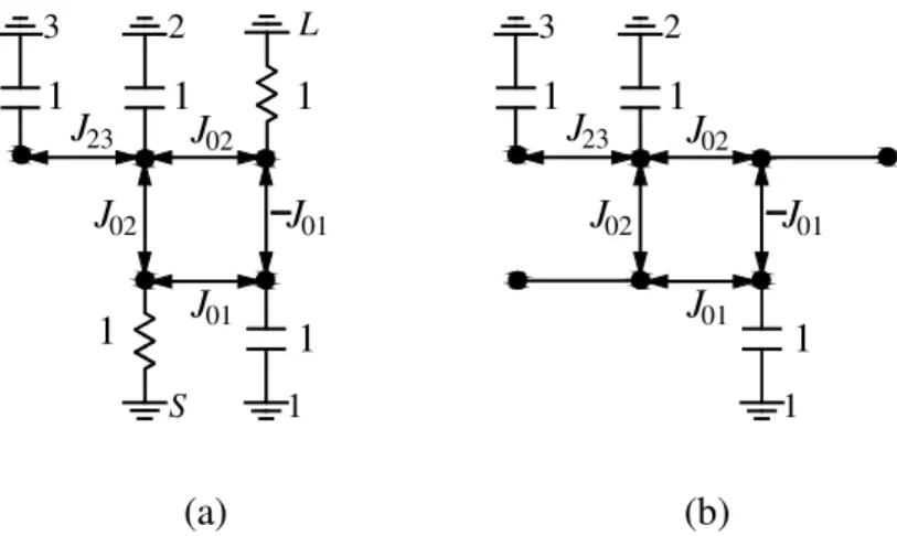
Broadband response.---55 Fig. 4.1 Two in-line fourth-order filters with two tapped input/output schemes:
symmetric (A–B) and skew-symmetric (A–B’) feeds.---57 Fig. 4.2 Generic coupling structure of the in-line bandpass filter.---58 Fig. 4.3 Coupling coefficients of two stepped-impedance resonators against D1 for
various D2. L1 = L2 = 7.6, W1 = 0.4, W2 = 2.0, all in mm. Substrate: εr =
2.2, thickness = 0.508 mm.---59 Fig. 4.4 Simulation responses of the two fourth-order filters. (a) M-type: D12 =
D34 = 0.28, D23 = 1.0, Lf = 3.2. (b) E-type: D12 = D34 = 0.82, D23 = 0.37,
Lf = 3.2, all in mm.---62
Fig. 4.5 The equivalent circuit of two coupled resonators with coupling.---64 Fig. 4.6 Responses of ∠Y21 – ∠Y11 for investigating occurrence of the
transmission zeros of the E-type filter in Fig. 4(b). (a) Resonators 1 and 2, D2 = 0.82 mm. (b) Resonators 2 and 3, D2 = 0.37 mm. (c) Resonators 1
and 3, D2 = 3.19 mm.---66
Fig. 4.7 ∠Y21 – ∠Y11 responses for identification type of coupling between resonators 1 and 3. (a) D2= 0.6 mm. (b) D2 = 1.5 mm.---68
Fig. 4.8 |S21| responses based on coupling matrices in (4.2.11)---69
Fig. 4.9 Responses of higher-order in-line filters with m = e = 0.011.---70 Fig. 4.10 The moves of the tunable transmission zeros due to the slide of tap point
for the E-type filters with skew-symmetric feed.---71 Fig. 4.11 Analysis of fz1 and fz2. (a) Four-port network. (b) Responses for X21 of the
VIII
Fig. 4.12 X21 responses for the test circuit and the E-type circuit. (a) Test circuit. (b)
Skew-symmetric feed. (c) Symmetric feed.---72 Fig. 4. 13 (a) Group delay and S-parameter responses of the E-type filters with
symmetric feed. All circuit parameters are in Fig. 4.4(b). (b) Photo.----74 Fig. 4.14 Layout and performances of the E-type filters with skew-symmetric feed.
(a) Circuit layout. Dimensions in mm: L1 = 3.48, L2 = 3.78, L3 = 2.2, L4 =
1.48, L5 = 4.1, L6 = 1.5, Lf = 2.13, W1 = 0.2, W2 = 2.5, D12 = 0.6, D23 =
0.5. (b) Group delay, |S21| and |S11| responses.---76
Fig. 4.15 Layout and performances of the sixth-order E-type filters with skew-symmetric feed. (a) Circuit layout. Dimensions in mm: L1 = L2 =
6.32, Lf = 3.2, W1 = 0.2, W2 = 2.5, D12 = D56 = 0.14, D23 = D45 = 0.82, D34
CHAPTER 1
Introduction
High-performance bandpass filters with low loss, high selectivity, linear phase, compact size, and wide stopband are essential to design of the RF front-ends for modern wireless/microwave communication systems. For microwave coupled- resonator filters, frequency selectivity and phase responses are related to the arrangement of resonators, source, and load. Extensive research has been drawn to this study for decades. A survey of the major development can be found in [1-11].
It is well-known that coupled-resonators in a sequence can be only used to realize the filters with a maximally-flat or equal-ripple response [12]. If a number of routes can be arranged between the input and output terminations in the filter, the sum of the transmitted signals through different routes may vanish on the output port at certain frequencies. Therefore, transmission zeros can be generated at these frequencies and the rejection level of the stopband can be then improved. For example, a single transmission zero can be produced in a three-resonator filter if the first resonator is simultaneously coupled to the second and the third resonators [13]. The zero can be placed in either the upper or the lower rejection band depending on the phase relationship of the signals through different routes. A second well-known example is the quadruplet, which has a pair of transmission zeros on each side of the passband. Coaxial resonators [14] and circular cavities [15] are proposed to realize this configuration by bridging the first and the fourth resonating elements with negative cross-coupling, respectively. It is worth pointing out that there are four resonators in the equivalent circuit of the filter in [15] although there are only two
physical cavities. In fact, each circular cavity is a dual-mode resonator. This dual-mode cavity filter has several advantages including lower loss, reduced weight, and multiple transmission zeros. Eventually, filters of this type become a standard in satellite communication industry [16]. In [17-18], it is revealed that the in-band phase can be equalized if the pair of zeros is placed on the real axis in the complex frequency plane. For obtaining such zeros, positive cross-coupling must be established between the first and the fourth resonators.
Many complex structures for coupled-resonator filters have been proposed to achieve more stringent responses. Nowadays, applications can be found in virtually any type of microwave communication systems including satellite, terrestrial, and mobile communications. In section 1.1, the structures suitable for microwave coupled-resonator filters are briefly surveyed. The motivation and the contribution of this research are addressed in section 1.2 and 1.3, respectively. Finally, the outline of the dissertation is given in section 1.4.
1.1 The Structures of Coupled-Resonator Filters
Generally speaking, a lumped-element equivalent circuit can be used to model a coupled-resonator filter. Fig. 1.1 shows the equivalent circuit of a direct-coupled waveguide filter with N cavities [12]. Each mutual inductive coupling is used to model an iris on the conductive wall between cavities. It is noted that only adjacent resonators are mutually coupled. Filter based on this structure can have a maximally-flat or Chebyshev response, i.e. an all-pole response, since there is no finite transmission zero in the |S21| response. The impedance matrix of the equivalent
L L L L L vs 2 2 2 2 C RS M12 C M23 C L L 2 2 L RL C C M N-1,N
Fig. 1.1. The equivalent circuit of a direct-coupled waveguide filter with an all-pole response. Ω + Ω Ω Ω Ω + = − − − N N L N N N N S s i i i i i j R M j M j j j M j M j j M j M j j R v 1 3 2 1 , 1 , 1 23 23 12 12 . . . . 0 0 0 . . 0 0 0 . . . . . . . . . . . . . . 0 0 . . 0 0 0 . . 0 0 . . 0 0 0 . . 0 0 ω ω ω ω ω ω (1.1.1)
where i1, i2, i3, and i4 are the loop currents,
− = Ω ω ω ω ω 0 0 C L , ω0 =1 LC . For
narrow-band applications, it is noted that ωMi,j can be approximately by ω0Mi,j [12].
Equation (1.1.1) can be then expressed as
Ω + Ω Ω Ω Ω + = − + − N N N N N s i i i i i jg g j j jg jg j j jg j j jg g v 1 3 2 1 1 1 3 2 1 0 . . . . 0 0 0 . . 0 0 0 . . . . . . . . . . . . . . 0 0 . . 0 0 0 . . 0 0 . . 0 0 0 . . 0 0 (1.1.2)
The equivalence of (1.1.1) and (1.1.2) can be established if = ∆ 1 0 0 g g Z RS , ∆ = + 1 0 N N L Z g g
R ,Mi,j =∆ gigj for i≠ j, where Z0 is the port impedance.
The values of gn for 0≤n≤N+1can be determined by the maximally-flat insertion
loss and return loss functions:
( )
N S21 2 2 1 1 Ω + = Ω (1.1.3a)( )
N N S 2 2 2 11 1 Ω+ Ω = Ω (1.1.3b)where N is the filter order. It can be seen that |S21|2 decreases monotonically with Ω
when Ω > 1, and |S11|2 increases monotonically with Ω. A Chebyshev polynomial can
be used to specify the insertion loss and return loss of an N-order filter as
( )
( )
Ω + = Ω 2 2 2 21 1 1 N C S ε (1.1.4a)( )
( )
( )
Ω + Ω = Ω 2 2 2 2 2 11 1 N N C C S ε ε (1.1.4b)where the ripple level of the in-band |S21| response is 10log
(
1+ε2)
dB since theChebyshev polynomial CN(Ω) oscillates when −1≤Ω≤1. Design formulas for the
gn in (1.1.2) based on (1.1.3) and (1.1.4) can be found in [1] and [12].
Fig. 1.2 shows the equivalent circuit incorporating multiple mutual inductive coupling, and its impedance matrix can be expressed as [16]
24 M 1 H 1 F s v S R 2 2 H H 2 2 H H M13 1 F 12 M M23 14 M 1 F 2,N M 1 H 2 2 H H L R 1 F M 1 F N-1,N 1,N M
Fig. 1.2. The equivalent circuit of a direct-coupled waveguide filter incorporating multiple inductive coupling.
Ω + Ω Ω Ω Ω Ω + = − − − − − − − − − N N L N N N N N N N N N N N N N N N N S s i i i i i j R jM jM jM jM jM j j jM jM jM jM jM j jM jM jM jM jM j jM jM jM jM jM j R v 1 3 2 1 , 1 , 3 , 2 , 1 , 1 1 , 3 1 , 2 1 , 1 , 3 1 , 3 23 13 , 2 1 , 2 23 12 , 1 1 , 1 13 12 . . . . . . . . . . . . . . . . . . . . . . . . . . 0 0 . . 0 0 (1.1.5)
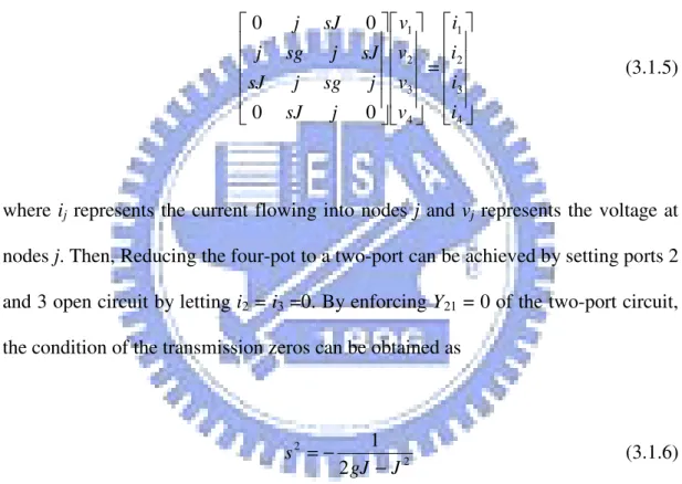
Each resonator is not only coupled to the neighboring resonators in sequence, but also non-adjacent resonators by cross-coupling. The matrix in (1.1.5) can be written in a compact form:
[ ] [ ]
Z = R + j(
Ω[ ] [
U + M]
)
(1.1.6)where [U] is anN ×Nidentity matrix, [R] has all zero entries except for (1, 1) and (N, N) elements. Matrix [M] is called the coupling matrix and has elements of Mi,j for
j
zeros [14-19]. It is known that an impedance K-inverter, which can be equivalent to an inductive coupling element, is defined as [12]
= 2 1 2 1 0 0 i i jK jK v v (1.1.7)
By using the impedance K-inverter, the coupling between source/load and resonators can be taken into account by an extended (N+2)×(N+2) matrix. In addition, it may be necessary to replace the frequency variable jΩ by j(Ω+Xi) for the (i, i) element in
(1.1.5) if transmission zeros are not in pairs, i.e. the |S21| response is asymmetric with
respect to the center frequency. Then, (1.1.5) is transformed to
(
)
(
)
(
)
+ Ω + Ω + Ω = + + + + + + + + + 1 2 1 0 1 , 1 , 2 1 , 1 1 , 0 1 , , 2 , 1 , 0 1 , 2 , 2 2 12 02 1 , 1 , 1 12 1 01 1 , 0 , 0 02 01 . . 1 . . . . . . . . . . . . . . . . . . . . . . . . 1 0 0 . . 0 0 N N N N N N N N N N N N N N N N N N N s i i i i i jK jK jK jK jK X j jK jK jK jK jK X j jK jK jK jK jK X j jK jK jK jK jK v (1.1.8)This matrix can be written in a compact form as
[ ]
Z =[ ]
R + j(
Ω[ ] [ ]
U + K)
(1.1.9)1 vs K01 K12 S R jX 1 H 3 2 13 K 23 K K34 1 H jX 1 H jX RL
Fig. 1.3. The K-inverter equivalent circuit of a third-order filter.
[ ]
= + + + + + + + + 0 . . . . . . . . . . . . . . . . . . . . . . . . 0 1 , 1 , 2 1 , 1 1 , 0 1 , , 2 , 1 , 0 1 , 2 , 2 2 12 02 1 , 1 , 1 12 1 01 1 , 0 , 0 02 01 N N N N N N N N N N N N N N N N N K K K K K X K K K K K X K K K K K X K K K K K K (1.1.10)This matrix is frequently employed for synthesis of the waveguide filters since iris coupling between waveguide cavities can be properly modelled by the K-inverter. If the frequency variable Ω is viewed as a 1-H inductor, the lowpass prototype of a lossless filter can be obtained. For example, Fig. 1.3 shows the equivalent circuit of a lossless third-order filter with non-adjacent impedance inverter K13.
For strip-transmission-line filters, however, the admittance matrix with J-inverters may be more suitable and can be expressed as [20]
(
)
(
)
(
)
+ Ω + Ω + Ω = + + + + + + + + + 1 2 1 0 1 , 1 , 2 1 , 1 1 , 0 1 , , 2 , 1 , 0 1 , 2 , 2 2 12 02 1 , 1 , 1 12 1 01 1 , 0 , 0 02 01 . . 1 . . . . . . . . . . . . . . . . . . . . . . . . 1 0 0 . . 0 0 N N N N N N N N N N N N N N N N N N N s i i i i i jJ jJ jJ jJ jJ B j jJ jJ jJ jJ jJ B j jJ jJ jJ jJ jJ B j jJ jJ jJ jJ jJ v (1.1.11)where the J-inverter is defined as [12] = 2 1 2 1 0 0 v v jJ jJ i i (1.1.12)
The matrix in (1.1.11) can be expressed as
[ ]
Y =[ ]
G + j(
Ω[ ] [ ]
U + J)
(1.1.13)where [G] has all zero elements except the (1, 1) and (N+2, N+2) elements, and
[ ]
= + + + + + + + + 0 . . . . . . . . . . . . . . . . . . . . . . . . 0 1 , 1 , 2 1 , 1 1 , 0 1 , , 2 , 1 , 0 1 , 2 , 2 2 12 02 1 , 1 , 1 12 1 01 1 , 0 , 0 02 01 N N N N N N N N N N N N N N N N N J J J J J B J J J J J B J J J J J B J J J J J J (1.1.14)If the frequency variable Ω is viewed as a 1-F capacitor, the lowpass prototype can be thus obtained. A third-order lowpass prototype is shown in Fig. 1.4, which is the dual of the circuit in Fig. 1.3.
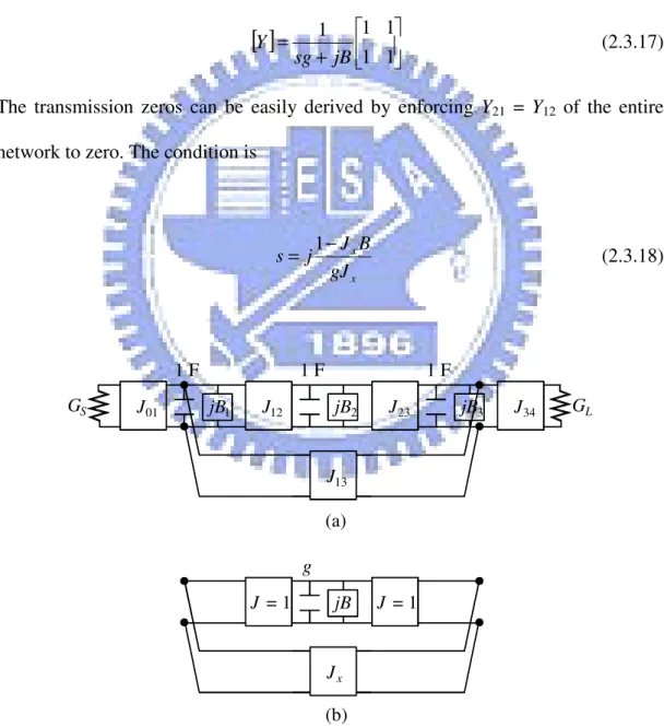
The structures proposed to realize the filters with transmission zeros can be expressed by the coupling matrix [M] in (1.1.5), the K-inverter matrix [K] in (1.1.10), or the J-inverter matrix [J] in (1.1.14). Since the matrix [J] is particularly suitable for strip-transmission-line filters, and microstrip filters are used in the experiment in this study, the J-inverter equivalent circuit are adopted.
1 F J jB S
i
s G J01 1 12 1 F J jB J GL jB 14 J 2 23 3 34 1 FFig. 1.4. The J-inverter equivalent circuit of a third-order filter.
2 2 J F F
i
s L 4 1 S (b) 14 J 23 1 1 g F 1 1 1 g 1F 1 1 1 S 4 L (c) 2 3 J J 1 S 2 g 3 g (a) si
J01 1F 1 J14 23 J12 L 4 45 J 1F 1 34 1F 2 3 1F ' 'Fig. 1.5. The quadruplet filter. (a) The simplified form of the equivalent circuit. (b) The alternative equivalent circuit. (c) The coupling diagram.
For most of the practical microwave filters with transmission zeros, only a few non-adjacent coupling elements are required to establish. Take the quadruplet filter as an example [14, 15, 17-19, 21-23], Fig. 1.5(a) shows the simplified form of the equivalent circuit with six J-inverters: J01(J45=J01), J12(J34=J12), J14 and J23. Note that
J13 and J24 inverters are not necessary in this network. Fig. 1.5(b) shows the
alternative equivalent circuit, where the J01 and J12-inverters are normalized to unity
and the capacitances are changed accordingly. The equivalence between Fig. 1.5(a)
and 1.5(b) can be established ifJ01 =1 g1 ,
2 1 12 1 g g J = , 2 23 23 J' g J = , and 1 14 14 J' g
J = . They can be obtained from the operations on the rows and columns of the following matrix.
[ ]
= 0 0 0 0 0 0 0 0 0 0 0 0 0 0 0 0 0 0 0 0 0 0 0 0 45 45 34 14 34 23 23 12 14 12 01 01 J J J J J J J J J J J J J (1.1.15)Fig. 1.5(c) plots the coupling diagram of the quadruplet, where the solid and the dashed lines represent mainline and cross coupling, respectively.
A number of coupling configurations based on the quadruplet (CQ) are devised for achieving a response with multiple pairs of transmission zeros [24-25]. The examples include the canonical form [24] and cascaded quadruplet (CQ) [25]. Fig. 1.6(a) and (b) plot the coupling diagrams, respectively. In these structures, multiple pairs of transmission zeros can be placed on the real axis or the imaginary axis. It is noted that no reactive element is added to the diagonal elements of the matrix [J], i.e. Bi = 0 for 1≤i ≤N, since the distribution of transmission zeros are symmetric with
1 L 1 S 1 S (i) S 3 2 (g) 1 L (h) L 2 S 3 (e) L 4 L S 2 (f) 2 3 (b) (a) 1 2 (c) 2 1 S 3 (d) L S 4 2 1 3 L 6 5 S 1 2 6 2 3 4 3 S 1 4 5 L 5 7 8 L
Fig. 1.6 Various coupling diagrams. (a) The canonical form of a sixth-order filter. (b) An eighth-order CQ filter. (c) The trisection filter. (d) A fifth-order CT filter. (e) A third-order filter with the source coupled to resonators 1 and 3. (f) A second-order filter with the he source coupled to resonators 1 and 2. (g) A second-order filter with source-load coupling. (h) The canonical form of a fourth-order filter with source-load coupling. (i) An extended doublet.
When the response is asymmetric with respect to the center frequency, the extracted-pole structure [26] and the trisection [27, 28] are proposed to realize a single transmission zero, respectively. The cascade trisection (CT) is useful for the higher order filters with an asymmetric response and multiple transmission zeros. Such filters can be applied to cellular base stations since the rejection on one side is more stringent than the other. Fig. 1.6(c) and (d) shows the coupling diagrams of the single trisection and a fifth-order CT filter, respectively.
In [29-31], the coupling from source/load to two resonators is proposed. For a third order network, a pair of transmission zeros can be generated if the source is simultaneously coupled to the first and the third resonators, as shown in Fig. 1.5(e) [29]. Compared with the quadruplet, the number of the resonators is reduced by one. For a second order network, a single transmission zero can be created if the source is coupled to two resonators, as shown in Fig. 1.5(f) [30]. Compared with a trisection, the number of resonators is reduced by one. An adaptive synthesis of coupled-resonator filters with source/load to multi-resonator coupling can be found in [31].
If direct coupling exists between source and load, it is shown that at most N/2 pairs of zeros can be generated for the canonical form with an N-even order [32-34]. Fig. 1.6(g) and (h) shows the coupling diagrams of the second-order and the fourth-order canonical form, respectively. The extended-doublet structure shown in Fig. 1.6(i) is a second realization of a third order filter with a pair of zeros [35, 36]. It consists of a main doublet attached by an additional resonator. The source and the load are coupled to two resonators in the main double. It is noted that the sign of one of the four coupling elements must be opposite to the others for generating a pair of
zeros. Waveguide cavities [35] and microstrip resonators [36] have been proposed to realize this structure.
1.2 Motivations
The motivation of this work roots in noting that many innovative coupled-resonator bandpass filters have been proposed to generate plural transmission zeros with fewer resonators [29-38]. Increasing number of transmission zeros around the passband can enhance the frequency selectivity so that the number of resonators can be reduced. This is accompanied with several advantages including lower insertion loss and a more compact circuit size. Many techniques have been proposed, which include source/load to multi-resonator coupling [29-31, 35, 36], source-load coupling [32-34], non-resonating nodes [35] and frequency-dependent coupling [37, 38].
In [29], a particular coupling scheme is arranged for source/load terminations and a triple-mode cavity to realize a third-order filter with a pair of zeros. In [30], the source and the load of a dual-mode resonator filter are designed to couple simultaneously to two resonators for creating two independently controllable zeros. In [34], fourth-order canonical microstrip filters with source-load coupling are developed to two pairs of zeros. In [35, 36], it is shown that an extended-doublet can generate a pair of zeros for a third-order filter. In [35], second and third-order coupled-cavity structures that can generate a pair of zeros can be cascaded by non-resonating nodes for higher-order waveguide filters with plural zeros. Note that all the structures involve source/load to multi-resonators coupling or source-load coupling. Theoretically, for a coupled-resonator filter of order N with
frequency-independent coupling, the maximum number of finite transmission zeros is at most N [32].
However, the number of transmission zeros can be increased by one if frequency-dependent coupling is used [37, 38]. In [37], a third-order waveguide filter is reported to have four zeros. The frequency-dependent coupling element consists of iris and waveguide stub element. Unfortunately, this structure can not be easily applied to transmission-line resonators. In [38], a second-order combline filter with a frequency-dependent dielectric capacitor between source and load is reported to have three zeros. It is noted that a general synthesis for the filters with frequency-dependent coupling has not been reported yet. This research aims at exploring frequency-dependent coupling structures capable of generating transmission zeros. In addition, filter synthesis with frequency-dependent coupling is developed.
From cost and circuit integration consideration, microstrip realization of bandpass filters has gained much attention [10]. The reduction of number of resonators is especially important to microstrip resonators since they have a relatively low quality (Q) factor. Many coupling diagrams have been applied to microstrip filters [22, 23, 28, 34, 36]. In [22, 23], a microstrip quadruplet is achieved by open-loop resonators. In [28], a fifth-order cascade trisection filter is realized by hairpin resonators. In [34], a short coupled-line is placed between input and output ports to introduce source-load coupling. In [36], a particular microstrip two-mode resonator accompanied by a hairpin resonator is proposed to realize a third-order filter with a pair of zeros.
In this work, microstrip frequency-dependent coupling structure is devised. Based on this structure, a microstrip trisection filter can have a pair of transmission zeros without using via-hole grounding, dual-mode resonating elements, and non-resonating nodes. Besides, source/load to multi-resonator coupling and source-load coupling are not required at all. Furthermore, the third-order filter can have two additional zeros created by tapped-line.
1.3 Contributions
A novel zero-generating structure with frequency-dependent coupling structure is developed. It has several attractive properties. First, the design is simple since the condition of zeros involves only two elements: a resonator and a frequency-dependent admittance inverter. Second, in the admittance matrix of the lowpass prototype, all diagonal elements are not required to add any reactive elements. Third, the trisection can be directly cascaded to other resonators by cross-coupling for higher order filters without using non-resonating nodes [35] or external components [38]. The formula of the lowpass prototypes with the proposed structure is developed. Microstrip filters of order N = 3 and 4 is designed to have at most four and five zeros, respectively.
It is found that this frequency-dependent coupling also exists among stepped-impedance resonators [39, 40] in a compact inline arrangement. All resonators form an in-line array so that the circuit occupies a compact area. When order is increased, the circuit size grows only in the direction of the width, which is usually much smaller than the length of the resonator. Furthermore, certain transmission zeros in the filter response can be generated by the nonadjacent
frequency-dependent coupling. Transmission zeros on both sides of the passband for fourth-, sixth-order filters are created by using proper non-adjacent coupling. Enhanced attenuation rate in transition bands is thus obtained.
Although the circuit layout looks quite similar to that of a combline structure, it needs neither lumped element nor grounding via, so that filter fabrication is easier and more reliable. The price paid for the full-length resonators is that circuit area is slightly larger than twice the size of a quarter-wave combline counterpart. The use of full-length resonators, however, brings one more degree of freedom to circuit designers in choosing symmetric or skew-symmetric feed [41]. It will be shown that existence and location of certain zeros are subject to the symmetry used in the tapped input/output arrangement. It is demonstrated for the particular in-line structure that the extra zero can be placed in lower and upper stopbands by symmetric and skew-symmetric feeds, respectively.
1.4 Organization of the Dissertation
Chapter 2 reviews the derivation of the general Chebyshev filtering function and the synthesis of several basic coupling schemes including quadruplet, trisection, and extended doublet. A novel zero-generating structure with frequency-dependent coupling is described in chapter 3. Three novel lowpass prototypes with a pair of transmission zeros are developed based on this structure. The design of the microstrip frequency-dependent J-inverter is given. The comparison of measured responses of experimental circuits with simulation data is also presented. In chapter 4, inline stepped-impedance resonator filters are explored. The existence of the zeros is studied in terms of Y-parameter matrix by taking the adjacent and nonadjacent
coupling into account. Creation of zeros by the tapped input/output structure is also investigated. Experiment is conducted to validate the theory. Finally, chapter 5 gives the conclusion.
CHAPTER 2
Fundamental of Admittance Matrix Synthesis
In this chapter, synthesis of the admittance matrix for a filter with the general Chebyshev function is reviewed. Section 2.1 describes the technique for generating the Chebyshev polynomials with finite transmission zeros [11, 42]. Section 2.2 describes how to derive the ABCD matrix from the general Chebyshev filtering function. Finally, section 2.3 gives the synthesis of the admittance matrices for some basic coupling diagrams including quadruplet, trisection, and extended-doublet.
2.1 General Chebyshev Filtering Function
The general Chebyshev filtering function can be described by
( )
cos cos(
( )
)
, 1 1 1 ≤ =∑
= − ω ω ω N n n N x C (2.1.1)( )
cosh cosh(
( )
)
, 1 1 1 ≥ =∑
= − ω ω ω N n n N x C (2.1.2)( )
n n n x ω ω ω ω ω − − = 1 1 (2.1.3)where jωn = sn is the location of the nth transmission zero in the complex plane.
Since xn(1) = 1 and xn(–1) = –1, it is easily verified that CN(ω) oscillates between –1
and 1. It is noted that CN(ω) degenerates to the conventional Chebyshev function
transmission zeros nfz must be ≤N . The general Chebyshev function can be
transformed to a polynomial by the operations as follows.
( )
(
( )
)
(
)
+ = =∑
∑
= = − N n n n N n n N x a b C 1 1 1 ln cosh cosh cosh ω ω (2.1.4)( )
n n n n x a ω ω ω ω ω − − = = 1 1 and( )
n n n n x b ω ω ω ω ω ω − − ′ = − = 1 1 1 2 2 (2.1.5)whereω′= ω2−1. Then (2.1.4) is transformed into
( )
( ) ( )(
)
(
)
+ + + = ∑ + ∑ =∏
∏
= = + − + = = N n n n N n n n b a b a N b a b a e e C N n n n N n n n 1 1 ln ln 1 2 1 2 1 1 1 ω (2.1.6)If the numerator and the denominator of the second term in (2.1.6) is multiplied by
(
)
∏
= − N n n n b a 1 , we can obtain( )
(
)
(
)
− + + =∏
∏
= = N n n n N n n n N a b a b C 1 1 2 1 ω (2.1.7)Equation (2.1.7) can be further transformed into
( )
(
)
(
)
(
)
∏
∏
∏
= = = − − + + = fz n n n N n n n N n n n N d c d c C 1 1 1 1 2 1 ω ω ω (2.1.8) 1 n n c ω ω− = and 2 1 1 1 2 n n d = ω − − ω (2.1.9)It can be seen that the roots the denominator of CN(ω) are the transmission zeros.
The numerator of CN(ω) can be easily derived when N≤4. If N = 3, the numerator
of CN(ω) can be written as
( )
[
]
(
)
3 2 1 1 2 3 2 1 2 1 ( ) NumCN ω = cc +d d c + c d +cd d (2.1.10)If a transmission zero is placed at s = jω1, it is obtained that c1 = c2 = ω, d1 = d2 = ω’,
1 3 1 ω ω− = c , and 2 1 3 1 1 ω ω′ − = d . Then, (2.1.10) is derived as
( )
[
]
1 2 1 1 2 2 1 3 1 1 1 2 1 2 1 1 2 2 Num ω ω ω ω ω ω ω ω + − − − + − + − + = N C (2.1.11)Thus, the insertion loss function for a third-order filter with a transmission zero can be expressed as
( )
ω ε 2 3 2 2 21 1 1 C S + = (2.1.12) 0 1 0 1 2 2 3 3 3( ) a a b b b b C + + + + = ω ω ω ω ω (2.1.13)where the coefficients area0 =1, a1=−1ω1 , b0 =1/ω1,
2 1 1=−1−2 1−1ω b , 1 2 =−2 ω b , and b3 =2+2 1−1ω12 .
If a pair transmission zeros are symmetrically placed at s=±jω1on the
imaginary axis in the complex plane, then
1 1 1 ω ω+ = c , 2 1 1 1 1 ω ω′ − = d , 1 2 1 ω ω− = c , 2 1 2 1 1 ω ω′ − = d , =ω 3 c , and =ω′ 3 d . Then,
( )
[
]
− + − − + − = 2 1 2 1 2 1 3 1 1 2 1 1 1 2 1 2 Num ω ω ω ω ω ω N C (2.1.14)The general Chebyshev function for a third-order filter with a pair of zeros at
1
ω
j
s=± can be thus expressed as
0 2 2 1 3 3 3( ) a a b b C + + = ω ω ω ω (2.1.15)
where the coefficients area0 =1, 2 1 2 =−1ω a , 2 1 1=−1−2 1−1ω b , and 2 1 2 1 3 =2−1 ω +2 1−1ω b .
If the pair of zeros is placed on the real axis ats=±ω1, it is easy to obtain the
coefficient:a0 =1, 2 1 2 =1ω a , b1 =−1−2 1+1ω12 , and 2 1 2 1 3 =2+1 ω +2 1+1ω b .
The general Chebyshev function for a fourth-order filter with a pair of zeros at
1
ω
j
s=± can be derived in a similar manner and be expressed as
0 2 2 0 2 2 4 4 4( ) a a b b b C + + + = ω ω ω ω (2.1.16)
where a0 =1, 2 1 2 =−1ω a , b0 =1, 2 1 2 1 2 =−4+1ω −4 1−1ω b , and
(
)
2 1 2 1 4 =2+21−1ω +4 1−1ω b .In fact, the higher order Chebyshev polynomials with plural transmission zeros can be obtained by a recursive procedure [42]. The algorithm starts with
1 1 1 ) ( ω ω ω = − U and 2 1 1 1 1 ) ( ω ω = − V (2.1.17)
where the s = jω1 is the location of the first zero. Then, the process continues with
the following equations until all the zeros are used.
(
1)
1 1 ( ) ) ( 1 ) ( 2 1 2 1 ω ω ω ω ω ω ω − − + − − − = n n n n n U V U (2.1.18) ) ( 1 1 ) ( 1 ) ( 1 2 1 ω ω ω ω ω ω − + − − − = n n n n n V U V (2.1.19)If the order of the general Chebyshev function is N, the numerator can be expressed as
( )
[
ω]
( )
ω N N U C = Num (2.1.20)This algorithm can be programmed for computers without difficulties. In summary, the general Chebyshev filtering function with a total of nfz zeros can be expressed by
2.2 Synthesis of the ABCD Matrix
The next step to synthesize the admittance matrix of a filter is to obtain the ABCD parameters, which are assumed functions of complex frequency variable s. The derivation starts from obtaining the S21(s) from the insertion loss function by
substituting (–js) for ω
( )
( )
js C s S N =− + = ω ω ε2 2 2 21 1 1 (2.2.1)To form the function S21(s) from the given
( )
2 21 s
S , the right half-plane poles are rejected, and the left-plane poles are used to derive
( )
( )
( )
s F s P s S I ε = 21 (2.2.2)where polynomial P(s) and F(s) are normalized so that their highest coefficients are unity, and εΙ can be derived by
( )
( )
s s j F s P I = =ε ε (2.2.3)In a similar manner, the function S11(s) can be obtained from
( )
( )
( )
js C C s S N N − = + = ω ω ε ω ε 2 2 2 2 2 11 1 (2.2.4)Noting that S21(s) and S11(s) must have the same denominator, S11(s) can be expressed as
( )
( )
( )
s F s E s S R ε = 11 (2.2.5)where the polynomial E(s) is also normalized so that the highest coefficients are unity. If there are zeros at infinity, i.e. nfz < N, it can be seen that S11
( )
s =±1 when s approaches infinity. Thus, we have =±1R
ε since the highest coefficients of E(s)
and F(s) are unity. This condition holds for most cases studied in this research. Based on the conversion from S-parameters to ABCD parameters, the ABCD matrix for a filter with the general Chebyshev response can be expressed as
[
]
( )
( )
( )
( )
= s D s C s B s A s P ABCD I ε ) ( 1 (2.2.6)The polynomials A(s), B(s), C(s), and D(s) can be generally expressed as
( )
Im(
)
Re(
)
Im(
)
2 ... 2 2 1 1 1+ + + + + + = − − − − − − N N N N N N N N N f s e f s j e f s e j s A (2.2.7)( )
Re(
)
Im(
)
Re(
)
2 ... 2 2 1 1 1+ + + + + + = − − − − − − N N N N N N N N N f s j e f s e f s e s B (2.2.8)( )
Re(
)
Im(
)
Re(
)
2 ... 2 2 1 1 1− + − + + − = − − − − − N− N N N N N N N N f s j e f s e f s e s C (2.2.9)( )
Im(
)
Re(
)
Im(
)
2 ... 2 2 1 1 1− + − + + − = − − − − − N− N N N N N N N N f s e f s j e f s e j s D (2.2.10)0 1 2 2 1 1 ... ) (s s e s e s es e E N N N + + + + + = − − (2.2.11) 0 1 2 2 1 1 ... ) (s s f s f s f s f F = N + N N− + + + + − (2.2.12)
Noting that εR = 1 in (2.2.5), it can be observed that B(s) is of degree N, A(s) and D(s)
are of degree N-1. Since the network is reciprocal, the degree of C(s) must be N–2. This matrix is suitable for a network of even-N degree. If the coefficient εR = –1, A(s)
and D(s) are still of degree N–1. However, C(s) and B(s) become the polynomials of degree N and N–2, respectively. This matrix is used for a network of odd-N degree.
If a pair of transmission zeros is specified at s = ± j3 and in-band ripple is 0.1dB for a filter of N = 3, the polynomials can be derived as A(s) = D(s) = 1.9007s2 + 1.73596, B(s) = 1.7877s, and C(s) = 2s3+3.3167s. For the purpose of network synthesis, the product of the constant terms in A(s) and D(s) is intentionally normalized to unity. This normalization leads to
z z N = 3 s = +/−j 3 N = 4 s = +/−j 2.3 -10 -5 -6 -4 -3 -2 -1 0 1 2 3 4 5 6 Normalized Frequency -40 |S | ,| S | (dB ) -60 -50 2 1 -30 1 1 -20 0
A(s) = D(s) = 1.0949s2 + 1 (2.2.13) B(s) = 1.0298s (2.2.14) C(s) = 1.1521s3+1.9106s. (2.2.15)
Fig. 2.1 plots the |S21| and |S11| responses of this filter. Also shown in Fig. 2.1 is the
responses for a filter of N = 4 with a pair of transmission zeros at s = ± j2.3 and in-band ripple is 0.1dB, the polynomials are as follows: A(s) = D(s) = 1.7807s3 + 2.0487s, B(s) = 2s4 + 3.6378s2 + 1.0559, C(s) = 1.5854s2 + 0.7791. For enforcing the product of the constant terms in B(s) and C(s) to unity, all the polynomials are multiplied by a constant 1.1025. Then, we obtain
A(s) = D(s) = 1.9633s3 + 2.2588s (2.2.16) B(s) = 2.2051s4 + 4.0108s2 + 1.1642 (2.2.17) C(s) = 1.7482s2 + 0.85896 (2.2.18)
It is noted that all the coefficients are real since the distribution of the roots of E(s) and F(s) is symmetric with respect to the real axis of the complex plane.
2.3 Synthesis of the Admittance Matrix
2.3.1 Quadruplet and Its Variants
Fig. 2.2 shows the generic block which is the basic structure for a quadruple to generate a pair of transmission zeros. The creation of transmission zeros is explained as follows. The circuit in Fig. 2.2 has two signal paths between input and output ports. One is by the Jx-inverter, which is realized by cross-coupling, and its
g g
J
= 1
J
aJ
= 1
J
x1 1 x J Ja
g
g
(a) (b)Fig. 2.2. The basic structure of a quadruplet. (a) The J-inverter circuit. (b) The simplified schematic.
[ ]
= 0 1 1 0 x jJ Y (2.3.1)The other path is a cascade of two unitary J-inverters, two shunt capacitors g with an in-between Ja-inverter. Y-parameter matrix of this path from the input to the output
can be expressed as
[ ]
− − + = a a a a j gs J j J gs J s g J Y 12 2 (2.3.2)The transmission zeros can be obtained by enforcing Y21 = Y12 of the entire network
to zero. The condition can be explicitly expressed as [21-23]
2 2 (1 ) g J J J J s x a x a − = (2.3.3)
axis in the complex frequency plane at s = ±jΩzif the relation Ja/Jx < 0 holds since
1–JxJa > 0. On the other hand, the zeros can be shifted to s = ±Ωzby simply
reversing the sign of Ja/Jx. The ABCD matrix of the whole circuit can be expressed
as + + + = s K J g J K s K J g J K J s K J g s K J g s K J g J j D C B A a a a x a a a a x 2 2 2 2 2 2 2 1 (2.3.4)
where K = JxJa–1. The ABCD matrix can be used in the synthesis of a filter based on
this block.
Fig. 2.3 plots three possible schematics based on the zero-generating block described by (2.3.4). The circuit in Fig. 2.3(a) is the conventional quadruplet, the ABCD matrix of which can be expressed as
a J a a J J 1 g S S 1 4 L g 1 Jx 1 1 1 01 1 1 g 1 1 1 1 J L S L 1 J 1 x J x 1 1 1 1 1 g g 2 3 g g 3 2 1 g 2 g (a) (b) (c)
Fig. 2.3. The quadruplet and its variants. (a) The conventional quadruplet. (b) The circuit in which the load is simultaneously coupled to two resonators. (c) The circuit including the source-load coupling.
( )
( )
g s K J K J g s K J g g s D s A a a a + + = = 1 3 2 1 (2.3.5)( )
(
(
)
)
a a x a a J K s J g g J g g K J s K J g g s B = + + + + 2 2 2+ 1 2 2 1 4 2 2 1 1 1 (2.3.6)( )
K J s K J g s C a a + = 2 2 (2.3.7)Comparing the coefficients in (2.3.5-7) with those in (2.2.16-18), one can obtain the element values.
The circuit in Fig. 3(b) is a third-order filter with a pair of transmission zeros. Although the load is requited to simultaneously couple to the first and the third resonators, the number of the resonators is reduced by one. The ABCD matrix can be expressed as
( )
+ + = a a x J K s K J g J g g J s A 2 2 2 1 01 1 (2.3.8)( )
+ + = s K J g K g J s K J g g J s B a a a 1 3 2 1 01 1 (2.3.9)( )
s K J g J s C a 01 = (2.3.10)( )
+ = K J s K J g J s D a a 2 2 01 (2.3.11)By comparing (2.3.8-11) and (2.2.13-15), the element values can be determined. The circuit in Fig. 3(c) uses only two resonators to achieve a pair of transmission zeros. However, this structure can not be directly cascaded with other resonators. In addition, the design of source-load coupling may not be as well-known as that of the
inter-resonator coupling. It is noted that εR is no longer unity, which will be
determined by the |S21| level at infinity.
2.3.2 Extended-Doublet
Another three-resonator structure to produce a pair of zeros is the extended-doublet, as shown in Fig. 2.4(a). The generic block to produce a pair of zeros is shown in Fig. 2.4(b). It is noted that the generic block of the extended doublet requires three resonators. In fact, the resonator number compared with that of a quadruplet is increased by one. The generic structure can be analyzed as follows. The Y-parameter matrix of the route through resonator 1 can be expressed as
[ ]
− − = 1 1 1 1 2 01 s J Y (2.3.12)The other route with two resonators can be expressed as
[ ]
+ = 1 1 1 1 2 23 2 02 s J s J Y (2.3.13)The transmission zeros can be obtained by enforcing Y21 = Y12 of the entire network
to zero. The condition can be explicitly expressed as
2 01 2 02 2 23 2 01 2 J J J J s − = (2.3.14)
02 J 1 J23 1 3 1 1 S J02 23 J 02 J 1 01 J 01 J J01 1 J02 J01 1 L 1 2 1 2 3 1 (a) (b)
Fig. 2.4. The extended-double. (a) The schematic. (b) The generic block to produce a pair of zeros.
It can be seen that the location of zeros is controlled by the sign ofJ022 −J012. The
ABCD matrix of the whole circuit can be expressed as
+ + + + + + − = 1 4 1 1 1 1 1 2 2 23 2 01 2 02 2 01 2 23 2 02 2 01 3 2 23 2 01 2 2 23 2 01 2 02 2 01 2 2 23 2 01 2 02 2 01 s J J J J J J s J s J J s J J J J s J J J J D C B A (2.3.15)
The structures in Fig. 2.3(b) and Fig. 2.4(a) can be used to generate a pair of zeros for a third-order filter. However, both schematics involve source/load to multi-resonator coupling. One may wonder whether it is possible to devise a third-order filter with only inter-resonator coupling to produce a pair of zeros.
2.3.3 Trisection
For completeness of this chapter, the analysis of the trisection is also presented. Fig. 2.5(a) shows that a shunt-connected pair sg+jB is placed between any two J-inverters. The generic structure for generating the single transmission zero is
plotted in Fig. 2.5(b). The Y-parameter of the cross-coupling path can be expressed as
[ ]
= 0 1 1 0 x jJ Y (2.3.16)The Y-parameter matrix of the other path is
[ ]
+ = 1 1 1 1 1 jB sg Y (2.3.17)The transmission zeros can be easily derived by enforcing Y21 = Y12 of the entire
network to zero. The condition is
x x gJ B J j s= 1− (2.3.18) (b) x J GS J jB J jB J jB J GL (a) J = 1 g jB J = 1 12 01 1 J13 2 23 3 34 1 F 1 F 1 F
Fig. 2.5. The conventional trisection. (a) The J-inverter circuit. (b) The generic structure to produce a single transmission zero.
Since g > 0 and 1–JxB > 0, the single zero can be placed in the upper rejection band
if Jx > 0. On the contrary, the single zero can be placed in the lower rejection band
when Jx < 0. The ABCD matrix of the structure in Fig. 2.5(b) can be expressed as
(
)
− − + − + − = 1 2 1 ) 1 ( 1 2 JB jJ s gJ jB sg B J s jgJ D C B A x x x x (2.3.19)From (2.1.13), one can derive the ABCD matrix for a third-order filter with 0.1-dB in-band ripple and a single transmission zero at s = j3.
+ − − + − − + − = 1 2974 . 0 2476 . 1 4796 . 0 1652 . 2 2207 . 0 2868 . 1 3692 . 0 2095 . 1 1 2974 . 0 2476 . 1 2 2 3 2 s j s j s s j s j s s j s D C B A (2.3.20) Based on (2.3.19), the admittance matrix can be directly obtained as
[ ]
+ − + = 1 9847 . 0 0 0 0 9847 . 0 0668 . 0 8838 . 0 2899 . 0 0 0 8838 . 0 3053 . 0 8838 . 0 0 0 2899 . 0 8838 . 0 0668 . 0 9847 . 0 0 0 0 9847 . 0 1 j j j s j j j j s j j j j s j j Y (2.3.21)Then, the coupling coefficients and loaded Q factors for the coupled-resonator filter can be immediately obtained from (2.3.21).
CHAPTER 3
Synthesis and Microstrip Realization of Filters with
Frequency-Dependent Admittance Inverters
In this chapter, we explore a novel structure with frequency-dependent admittance J-inverter to generate a pair of transmission zeros. This configuration involves only two elements: a resonator and a frequency-dependent admittance inverter. In the admittance matrix of the lowpass prototype, all diagonal elements are not required to add any reactive elements. This property is different from that of a conventional trisection. Furthermore, the trisection can be directly cascaded to other resonators by cross-coupling. Section 3.1 explains the generation of a pair of zeros. Section 3.2 describes the synthesis of lowpass prototypes based on the proposed trisection. The element values are derived by comparing the coefficients of the polynomials in the two-port ABCD matrix with those derived from the general Chebyshev filtering function. Section 3.3 addresses the microstrip design of the J-inverters. Section 3.4 compares measured responses of experimental circuits with simulation data.
3.1 Frequency-Dependent J-Inverter for Generating a Pair of Zeros
Fig. 3.1 shows two possible blocks which can generate a pair of transmission zeros using frequency-dependent J-inverters. The frequency dependence is represented by a complex frequency variable s. The generation of transmission zeros is explained as follows. The circuit in Fig. 3.1(a) has two signal paths between input and output ports. One is the frequency-dependent J-inverter and the other is a cascade of two unitary J-inverters with a shunt capacitor C = sg in between. The
Y-matrix of the upper path is
[ ]
= 0 1 1 0 sJ Y (3.1.1)The lower path can be expressed as
[ ]
= 1 1 1 1 1 sg Y (3.1.2)The condition of transmission zeros can be obtained by enforcing Y21 = Y12 of the
entire network to zero and can be explicitly expressed as
Jg
s2 =− 1 (3.1.3)
It is evident that a pair of zeros can be symmetrically generated on the imaginary axis in the complex frequency plane at s = ±jΩz if the relation Jg > 0 holds andΩz =
1/√Jg. On the other hand, the zeros can be shifted to s = ±Ωzby simply inverting the
sign of Jg. The ABCD matrix of the whole circuit can be expressed as
sg 2 sJ J = 1 J = 1 J = 1 sg sJ 1 J = 1 J = 1 sJ sg 3 4 (a) (b)
Fig. 3.1. Two circuits with frequency-dependent J-inverter for generating a pair of zeros. (a) Single trisection. (b) Two trisections.


![Fig. 1.2 shows the equivalent circuit incorporating multiple mutual inductive coupling, and its impedance matrix can be expressed as [16]](https://thumb-ap.123doks.com/thumbv2/9libinfo/8230420.170885/17.892.169.810.285.827/equivalent-circuit-incorporating-multiple-inductive-coupling-impedance-expressed.webp)