Blue GaN-based vertical cavity surface emitting lasers by CW current
injection at 77K.
H. C. Kuo*, S. W. Chen, T. T. Kao, C. C. Kao, J. R. Chen, T. C. Lu, and S. C. Wang,
Department of Photonics and Institute of Electro-Optical Engineering,
National Chiao-Tung University, 1001 Ta Hsueh Rd., Hsinchu 30050, Taiwan
1. ABSTRACT
In the paper, we describe the fabrication and performance characteristics of GaN-based vertical-cavity surface-emitting lasers (VCSELs) by optical pumping and current injection. According to the employment of high-quality and high-reflectivity AlN/GaN DBRs in the whole structure, the lasing action of optically pumped GaN-based VCSELs with hybrid mirrors has been observed at room temperature. Due to the excellent results of optically pumped GaN-based VCSELs with hybrid mirrors, we further demonstrated the lasing behavior of GaN-based VCSELs by continuous-wave current injection at 77 K. The laser has one dominated blue wavelength located at 462 nm with a linewidth of about 0.15 nm and the threshold injection current at 1.4 mA. The divergence angle and polarization ratio of the GaN-based VCSELs with hybrid mirrors are about 11.7° and 80 %, respectively. A larger spontaneous coupling efficiency of about 7.5×10⁻² was also measured.
KEYWORDS: GaN, VCSEL, DBR, electrical pumping
2. INTRODUCTION
Wide band-gap alloys, especially in nitride-based materials, such as InGaN and AlGaN have been used in the commercial application of light-emitting devices including light-emitting diodes (LEDs), edge emitting laser diodes (LDs), and vertical-cavity surface-emitting lasers (VCSELs). These breakthroughs are mainly based on the improvement of crystal quality and the realization of p-type conductivity control [1], [2]. However, the development of GaN-based VCSELs is somehow slow compared with GaN-based LEDs and edge emitting LDs. Due to the lack of suitable substrates and the difficulty in growing high-quality and high-reflectivity GaN-based distributed Bragg reflectors (DBRs), the key problems are limiting the development of GaN-based VCSELs.
There are many excellent advantages of VCSEL compared with edge emitting LDs, such as circular output beam, low beam divergence, high modulation bandwidth, single longitudinal mode, and convenient wafer-level testing [3]−[5]. These advantages including high density optical storage system, laser printing, free space optical interconnects, fiber-optic communications, etc, make VCSELs promising optoelectronic devices for many practical applications. According to the breakthrough in the realization of nitride-based DBR, there are many research groups made efforts on the growth and fabrication of GaN-based VCSELs.
So far as optically pumped GaN-based VCSELs are concerned, there are only several reports in recent years [6]−[9]. In our previous study, optically pumped GaN-based VCSELs employed by double dielectric DBR [10], [11] and hybrid mirrors [12], [13] have been demonstrated. The related technology and characteristics of optically pumped GaN-based VCSELs will be discussed and shown in below [14]. Besides, although optically pumped GaN-based VCSELs were reported earlier, there has been no electrically pumped GaN-based VCSEL reports. Until our recent experimental results, they showed the lasing action of GaN-based VCSEL with hybrid mirrors at 77 K by continuous wave current injection [15]. We further measured the lasing characteristic including polarization, threshold energy density, the relative optical images, and so on. Thus, we will focus on the VCSEL with hybrid structure and discuss the characteristics of GaN-based VCSELs by optically pumped and electrically pumped.
Invited Paper
AIN/GaN DBRx5 AIN/GaN DBRx5 AIN/GaN DBRx5 AIN/GaN DBRx5
3. FABRICATION OF NITRIDE-BASED DBR
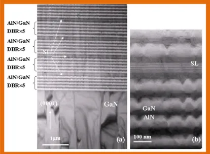
How to obtain high-reflectivity and large-stopband DBRs are the very important issues for nitride-based VCSELs. Our approach is using on the study of growing high-quality AlN/GaN DBRs. In our previous study, we reported the growth of crack-free AlN/GaN DBRs with insertion of 5.5 periods of AlN/GaN superlattice (SL) [16]. Fig. 1 shows cross-sectional transmission electronic microscopy (TEM) images of the SL DBR structure. The lighter layers represent AlN layers while the darker layers represent GaN layers. The interfaces between AlN and GaN layers shows sharply and abruptly in low-magnification TEM image, as shown in Fig. 1(a). The arrows indicate the SL insertion positions. Fig. 1(b) shows the cross-sectional TEM image of one set of 5.5-pairs AlN/GaN SL insertion layers under high magnification. Detailed observations by this TEM image reveal that the V-shaped defects in the AlN layers are always observable at the GaN-on-AlN interfaces and filled in with GaN. These V-shaped defects have been reported earlier and could be due to various origins such as stacking mismatch boundaries and surface undulation. The GaN/AlN SL insertion layers were ended by one more AlN layer to identify the changing from the AlN layer to the GaN layer. Here a set of GaN/AlN SL insertion layers can be seen as a quasi alloy of an AlxGa1-xN layer for a low refractive index quarter-wave layer in the
DBR structure.
Fig. 1. (a) Cross-sectional TEM image of the SL DBR structure. (b) Cross-sectional TEM image of the SL DBR structure. The 5.5-pair AlN/GaN SL can be observed clearly.
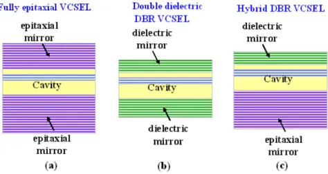
As we know, the nitride-based VCSELs structures can be classified into three major types due to the difficulty of growing high-quality and high-reflectivity nitride-based DBRs shown in Fig. 2. The first one is monolithic grown vertical resonant cavity consisting of epitaxially grown III-nitride top and bottom DBRs [Fig. 2(a)]. The advantage of the fully epitaxial microcavity is the controllable cavity thickness which is beneficial to fabricate microcavity structure. However, VCSELs require extremely high-reflectivity DBRs (i.e., high cavity Q factor). The fully epitaxial nitride microcavity is very difficult to achieve this requirement although the related results have been reported [17]. The second one is vertical resonant cavity consisting of dielectric top and bottom DBR [Fig. 2(b)]. The VCSELs with double dielectric DBR can exhibit high cavity Q factors because of the high-reflectivity DBR, which are relatively easy to fabricate. The large refractive index contrast in dielectric materials can make high-reflectivity and large-stopband DBR with less number of pairs. The drawback of the VCSEL with double dielectric DBR is the difficulty of controlling the cavity thickness precisely and the complicated fabrication process due to the employment of laser lift-off technique [10]. In addition, the thickness of the GaN cavity should keep as thick as possible to avoid the damage of the InGaN/GaN MQWs during the laser lift-off process. Such the thick cavity length could increase the threshold condition and reduce the microcavity
Fully epitxia1 VCSFL ep itaxia 1 mirror
C'vit
epitaxial i-niri or Double dielectric I)BR VCFL (liele CtriCmirror
(lie le etric mirro (a) (b)Hvliii:l Ji)BR V(ISFL
dielectric miii' or Cavity epitaxial rn.ir 101 (c)
effect [18], [19]. The final one is the VCSEL structure combining an epitaxially grown DBR and a dielectric type DBR which compromises the advantages and disadvantages of the above two VCSEL structures [Fig. 2(c)] [12], [13]. The VCSEL with hybrid DBR can eliminate the complex process and keep the feasibility of coplanar contacts with dielectric DBR mesas for the future electrically pumped VCSEL applications. The major requirement for the fabrication of VCSEL with hybrid DBR is to grow high-reflectivity and high-quality nitride-based DBRs. Our approaches to the realization of GaN-based VCSELs are mainly based on the VCSELs with double dielectric DBR and the VCSELs with hybrid DBR. The lasing action in VCSEL with double dielectric has been demonstrated by optical excitation in our previous studies [10], [11]. To achieve electrically pumped GaN-based VCSELs, we focus our study on the structure of VCSELs with hybrid mirrors in recent years. Since the problem of growing high-reflectivity nitride-based DBRs has been successfully overcome by inserting the AlN/GaN SL layers during the growth of AlN/GaN DBRs, it is expected that the higher possibility for achieving electrically pumped GaN-based VCSELs is based on the VCSEL structure with hybrid DBR.
Fig. 2. Three kinds of GaN-based VCSEL structures: (a) VCSELs with fully epitaxial DBR. (b) VCSELs with double dielectric DBR. (c) VCSELs with Hybrid DBR.
4. GAN-BASED VCSEL WITH HYBRID MIRRORS
The GaN-based VCSELs with hybrid mirrors were grown in a low-pressure high-speed rotating-disk metal organic chemical vapor deposition (MOCVD) system (EMCORE D75). Two-inch diameter (0001)-oriented sapphire substrates were used for the growth of AlN/GaN DBR and cavity. During the growth, trimethylgallium (TMGa), trimethylindium (TMIn), and trimethylaluminum (TMAl) were used as group III source materials and ammonia (NH3) as the group V
source material. Then, the growth process was as follows. The substrate was thermally cleaned in hydrogen ambient for 5 min at 1100°C, and then a 30 nm thick GaN nucleation layer was grown at 500°C. The growth temperature was raised up to 1100°C for the growth of a 2-µm GaN buffer layer. Then the 29 pairs of AlN/GaN DBR with six AlN/GaN superlattice insertion layers were grown under the fixed chamber pressure of 100 Torr similar to the previous reported growth conditions [16]. In order to reduce the tensile strain between the AlN and GaN, we inserted one superlattice into each five DBR periods at first twenty pairs of DBR. Then the superlattice was inserted into each three DBR periods for the remaining nine pairs of DBR to reduce the tensile strain. The overall AlN/GaN DBRs has 29 pairs with six superlattice insertion layers. On top of this 29-pair AlN/GaN DBR is a 790-nm-thick Si-doped n-type GaN cladding layer. The MQW active region consists of ten 2.5-nm-thick In0.2Ga0.8N QWs and 7.5-nm-thick GaN barrier layers. A
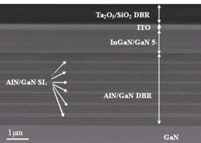
120-nm-thick Mg-doped p-type GaN cladding layer was grown on top of the MQWs to form a 5λ cavity in optical thickness for center wavelength of 460 nm. The MQWs were located at the antinode of light field in the microcavity for enhancing the coupling of photons and the cavity mode. During the growth, we use in-situ monitoring signals by fixing the monitor wavelength of 460 nm. Therefore, the thickness of each quarter-wavelength GaN and AlN can be precisely controlled by following the reflectance signals during the MOCVD growth. After the growth of nitride-based half cavity, an eight pairs of Ta2O5/SiO2 dielectric mirror was deposited by electronic beam evaporation as the top DBR reflector to
form the hybrid microcavity. To fabricate the electrically pumped hybrid VCSEL structure, an additional ITO layer was deposited on top of the cavity to serve as the transparent contact layer. Since the ITO locates within the VCSEL
microcavity, the thickness of ITO is set to 240 nm, corresponding to 1λ optical length in order to match the resonance phase condition of the microcavity. Fig. 3 shows the scanning electron microscopy (SEM) image of the whole hybrid VCSEL structure.
Fig. 3. Cross-sectional SEM image of the whole hybrid GaN-based VCSEL structure with hybrid DBRs, MQWs, and ITO layer.
For the development of semiconductor lasers, lasing action operated by optical pumping is the first step. The experimental results obtained from optically pumped VCSELs can be used to estimate the threshold condition of the designed VCSEL structure and provide better understanding of the material properties. Firstly, due to examine the reflectivity spectrum of the full VCSEL structure, we can assure the accuracy of the cavity thickness. Fig. 4 shows the room temperature reflectivity spectrum of whole microcavity by normal incidence measurement. According to the large refractive index contrast between Ta2O5 and SiO2 layers, the peak reflectivity is about 97 % with a large stopband of 70
nm. The irregular long wavelength oscillations of the reflectivity spectrum arise from the modulation of the respective top and bottom DBR spectra. In other words, the short wavelength oscillator is relatively regular, which only results from the top dielectric DBR since the short-wavelength light is absorbed by GaN layer. In Fig. 4, the photoluminescence (PL) emission spectrum of the full microcavity was measured at room temperature which is excited by a 325-nm He-Cd laser. Besides, the cavity resonance mode has a dominated wavelength at 464.2 nm with a full-width at half-maximum (FWHM) value of about 0.61 nm. The cavity mode dip is located at reflectivity curve corresponding to the emission peak. This indicates that the InGaN/GaN MQWs emission peak was well aligned with the hybrid microcavity. The cavity Q factor was estimated from the λ/Δλ to be about 760.
Fig. 4. Reflectivity spectrum at room-temperature and PL spectrum of GaN-based microcavity.
Fig. 5 (a). Laser output emission intensity as a function of the excitiation energy by VCSEL with hybrid DBR at room temperature. (b) Polarization of the laser under the pumping energy of about 82.5 nJ by the VCSEL with hybrid DBR. The solid red dot shows the experiment data and the dashed blue line shows the fitting curve.
In order to examine the lasing behavior, we measured the emission intensity of the microcavity with hybrid mirrors by increasing pumping power. Using a frequency-tripled Nd:YVO4 355-nm pulsed laser with a pulse width of ~0.5 nm at a
repetition rate of 1 kHz, the optical pumping of the samples was performed. In our experiment, the pumping laser beam with a spot size ranging from 30 to 60 μm was incident normal to the VCSEL sample surface. The light emission from the VCSEL sample was collected using an imaging optic into a spectrometer/CCD (Jobin-Yvon Triax 320 Spectrometer) with a spectral resolution of ~0.1 nm for spectral output measurement. Fig. 5(a) shows the emission intensity at room temperature from the GaN-based VCSEL with hybrid mirrors as a function of the excitation energy. A distinct threshold energy characteristic can be examed at the threshold excitation energy of ~55 nJ corresponding to an energy density of 7.8 mJ/cm2. Then, beyond the threshold, the laser output increased linearly by increased the pumping energy. Above the
threshold pumping energy, a dominant laser emission wavelength at 448.9 nm appears. The threshold density of this hybrid DBR VCSEL is relatively lower than that of our previous report [16], which may originate from the improvement of the reflectivity of the epitaxially grown AlN/GaN DBR inserted with SL layers. The laser emission spectral linewidth reduces as the pumping energy above the threshold energy and approaches 0.17 nm at the pumping energy of 82.5 nJ. To calculate the spontaneous coupling factor β of this cavity from Fig. 5(a), we normalized the vertical and horizontal scales and re-plotted it in a logarithm scale shown in the inset in Fig. 5(a). The difference between the heights of the emission intensities before and after the threshold roughly coincides with the value of [20]. The β value of this hybrid GaN-based VCSEL estimated from the inset of Fig. 5(a) is about 6×10². To estimating the β value, the alternative approach is based
on the approximation equation which can be expressed by [21], [22]
300 350 400 450 500 550 600 0 50 100 150 200 250 FWHM ~0.61 nm Wavelength (nm) PL Intensi ty ( arb. uni t) Cavity mode @ 464.2 nm 0 20 40 60 80 100 120 Reflec ti vi ty (%) 0 20 40 60 80 100 120 0 20 40 60 80 100 101 102 10-1 100 101 102 103 β~6X10⁻² N o rm a liz e d in te n s it y (a .u .) Excitation energy(nJ/pulse) Output po wer (ar b. un it )
Excitation Energy (nJ/pulse)
Room Temperature 0 30 60 90 120 150 180 210 240 270 300 330 Fitting data Experiment data
(a)
(b)
1 p p F F β = + (1) with , 2 3 3 4 /( / ) p c Q F V n π λ = (2)
where Fp is the Purcell factor; Q is the cavity quality factor; λ is the laser wavelength; Vc is the optical volume of laser
emission; n is the refractive index. So far as the photoluminescence spectrum of our hybrid DBR VCSEL having a narrow emission peak with full width at half maximum of 0.61 nm are concerned, cavity quality factor was estimated to be about 760. The refractive index is 2.45 for the GaN cavity. For the estimation of the optical volume and considering the penetration depth of the DBRs, we used the spot size of the laser emission image which was about 3 μm and the cavity length of about 9.5λ. The Purcell factor of about 2.9×10² was obtained and we estimated the β value to be about
2.8×10² by using these parameters, which has the same order of magnitude as the above β value estimated from the inset
in Fig. 5(a). This β value is three order of magnitude higher than that of the typical edge emitting semiconductor lasers (normally about 104~105 [22]) indicating the enhancement of the spontaneous emission into a lasing mode by the high
quality factor microcavity effect in the VCSEL structure. Fig. 5(b) shows the laser emission intensity as a function of the angle of the polarizer at the pumping energy of 82.5 nJ. The variation of the laser emission intensity with the angle of the polarizer shows nearly a cosine square variation. The result shows that the laser beam has a degree of polarization of about 89%, suggesting a near linear polarization property of the laser emission.
5. CHARACTERISTICS OF ELECTRICALLY PUMPED GAN-BASED VCSEL
Additional processes for current injection are necessary due to the fabrication of the VCSEL structure for electrical excitation. Because the epitaxially grown bottom AlN/GaN DBR was un-doped and non-conductive, we then processed the epitaxially grown wafer to form the intra-cavity co-planar p- and n-contacts for current injection. First, the mesa region was defined by photo-lithography and etched using an inductively coupled plasma reactive ion etching system with Cl2/Ar as the etching gases to expose the n-GaN layer for the n-contact formation. Then a 0.2-µm thick SiNx layer
was used as the mask to form a current injection and light emitting aperture of 10 μm in diameter, which was then deposited an ITO as the transparent contact layer. Since the ITO locates just next to the VCSEL microcavity, the thickness of 240 nm corresponding to 1λ optical length (λ = 460 nm) has to be accurate to match the phase condition and reduce the microcavity anti-resonance effect. The ITO was annealed at 525oC under the nitrogen ambient to reduce the
contact resistance as well as to increase transparency thus reducing the internal cavity loss. A high transmittance of about 98.6% at λ = 460 nm was measured for the deposited ITO after the annealing. Then the metal contact layer was deposited by the electron beam evaporation using Ti/Al/Ni/Au (20/150/20/1000 nm) and Ni/Au (20/1000 nm) as the n-type electrode and p-type electrode to form co-planar intra-cavity contacts, respectively. Fig. 6(a) shows the schematic of hybrid GaN-based VCSEL structure. Fig. 6(b) shows the SEM image of the completed VCSEL devices. For VCSEL performance characterization, the fabricated VCSEL devices were diced into an individual device size of 120 µm × 150 µm and packaged into the TO-can. The packaged VCSEL device was mounted inside a cryogenic chamber for testing under the 77 K condition. Fig. 6(c) shows the optical microscopy image of a GaN-based VCSEL sample device at an injection current of 1 mA. We placed the GaN VCSEL sample inside a liquid nitrogen cooled chamber at 77K and tested under CW current injection condition using a CW current source (Keithley 238). The emission light was collected by a 25 µm diameter multimode fiber using a microscope with a 40× objective (numerical aperture = 0.6) and fed into the spectrometer (Triax 320). The system has a focal distance of 320 mm and a grating of 1800 g/mm with a spectral resolution of 0.15 nm. The output from the spectrometer was detected by a charge-coupled device (CCD) to record the emission spectrum. The spatial resolution of the imaging system was about 1 µm as estimated by the diffraction limit of the objective lens.
vi
(a)
InGaN/GaN MQWs ITO transparent contact
Ta2O5/SiO2 DBR
P-type contact
SiNxinsulating layer P-type GaN Bulk GaN AlN/GaN DBR N-type GaN Sapphire substrate N-type contact Current aperture p-contact n-contact (b) (c)
Fig. 6. GaN-based VCSEL with hybrid mirrors by electrical pumping. (a) The schematic diagram of the intra-cavity GaN-based VCSEL. (b) SEM image for the VCSEL with the intra-cavity with two co-planar p- and n-contacts for current injection. (c) The plane-view image of a GaN-based VCSEL chip at an injection current of 1 mA. The crack line under the p-contact wire bond was occurred during the chipping process.
400 440 480 520 560 0 20 40 60 80 100 Bottom DBR Reflec ti vity (%) Wavelength (nm)
(a)
Top DBR 440 445 450 455 460 465 470 0 1 2 3 4 454.3 nm Intens it y (arb. unit) Wavelength (nm)(b)
FWHM ~ 0.21 nm Q ~ 2163Fig. 7. (a) The reflectivity spectrum of top and bottom DBRs show that the highest peak reflectivity of bottom and top DBR is about 99.4% and 99%, respectively. (b) The PL spectrum of the GaN-based VCSEL at room temperature.
Fig. 7(a) shows the reflectivity spectrum of crack-free 29-pair AlN/GaN DBR with six SL insertion layers and 8-pair Ta2O5/SiO2 DBR, respectively. A high peak reflectivity of 99.4 % with a spectral band width of ~25 nm was observed
from 29-pair AlN/GaN DBR. The flat-topped stopband indicates the high crystal quality of the AlN/GaN DBRs. The 8-pair Ta2O5/SiO2 DBR shows a peak reflectivity of about 99% at 460 nm. The quality factor Q of the fabricated
GaN-based VCSEL with hybrid mirrors without the ITO layer was estimated from the PL spectrum of the VCSEL structure as shown in Fig. 7(b). The VCSEL structure was also excited by a CW 325 nm He-Cd laser with a laser spot size of about 1 µm in diameter. We estimated the cavity Q factor by λ/Δλ to be about 2.2×10³ from the PL emission peak
of 454.3 nm and a narrow linewidth of 0.21 nm. This Q value is larger than that of the previous optically pumped VCSEL structure, which may originates from the improvement of AlN/GaN DBR reflectivity and the better sample
quality. In other words, the Q value is slightly higher than the value obtained from the whole VCSEL structure with intra-cavity ITO contact layer due to the additional absorption loss of the ITO.
0.0 0.5 1.0 1.5 2.0 2.5 0 2 4 6 8 10 12 I-V L-I
Input Current (mA)
V oltage (V olt) I-V L-I 0.0 0.5 1.0 1.5 2.0 2.5 3.0 (a) Ou tp ut Pow er (a rb. un it ) 77 K
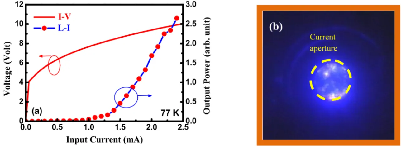
Fig. 8. (a) The laser output intensity as a function of injection current and current-voltage characteristics of GaN-based VCSEL under the CW condition at 77K. (b) Non-uniform emission images within the 10μm current aperture below the threshold.
Fig. 8(a) shows the light output power as a function of the injection current and current-voltage characteristics of the VCSEL sample at 77 K. The turn on voltage is about 4.1 V, which is indicated the well electrical contact of the ITO transparent layer and the intra-cavity structure. By calculation the serial resistance of the VCSEL, we found the value of serial resistance of the VCSEL about 1200 ohm when the driving current of 2.5 mA due to the small current injection aperture. The laser light output power showed a distinct threshold characteristic at the threshold current (Ith) of about 1.4
mA then increased linearly with the injection current beyond the threshold. The threshold current density is estimated to be about 1.8 KA/cm2 for a current injection aperture of 10 μm in diameter. The corresponding threshold carrier density is
about 2.6×1019 cm-3, estimated by assuming that the carrier lifetime of InGaN MQW is 6.4 ns and the internal quantum efficiency is 0.9 at 77K [23]. However, the injected carriers are not uniformly spreading over the whole 10μm current aperture from the spatial non-uniformity optical microscope image, as shown in Fig. 8(b) [12]. The actual area for carrier localizations appearing as those bright spots in the current aperture should be much smaller than the 10μm current aperture. We estimated the carrier localization area to be about 30~50% of the total aperture. Then the carrier density for the lasing spots should be in the range of 5.2×10¹⁹ to 8.7×1019 cm-3. We also estimated the threshold gain coefficient (g
th)
of our current injection VCSEL operated at 77K using the equation:
1 2 1 1 ln 2 eff a th i a a L d g d α d R R − ⎛ ⎞ ≥ < > + ⎜ ⎟ ⎝ ⎠ , (3)
where Leff is the effective cavity length, <αi> is the average internal loss inside the cavity, da is the total thickness of the
multiple quantum well and R1, R2 are the reflectivity of the top and bottom DBR mirrors, respectively. Because the
internal loss inside the cavity mainly came from the ITO absorption, we obtained a threshold gain coefficient value of about 8.8×103 cm-1, which is a reasonable value for the carrier density in the range of 5.2×10¹⁹ to 8.7×1019 cm-3.
Current aperture
(b)
455 460 465 470 475 480 0 1 2 3 4 5 6 1.2 1.4 1.6 1.8 2.0 2.2 2.4 0.14 0.16 0.18 0.20 0.22 0.24 0.26 Line wi d th (n m)
Input Current (mA) B C D E EL In te nsi ty ( a.u .) Wavelength (nm) 0.81 Ith Ith 1.31 Ith 1.71 Ith FWHM ~0.15 nm 10 μm Brightest spot 1 2 10-2 10-1 100 101 Curent (mA) In ten sit y (ar b . un it ) β ~7.5x10⁻² 77 K
(a)
(b)
Fig. 9(a). The laser emission spectrum under different injection carrier densities at 77 K; (Inset) The light emission linewidth at various injection carrier densities and the CCD image of the emission of the aperture. (b) The logarithm scale of light output intensity as a function of input current at 77 K. The two solid lines are guides to the eye.
Fig. 9(a) shows the laser emission spectrum under different injection carrier densities. Above the threshold current, only one dominant laser wavelength located at 462.8 nm appears. The inset figure shown in Fig. 9(a) shows the light emission linewidth under different injection carrier densities. Above the threshold current, the laser emission spectral linewidth reduces suddenly with the injection current and approaches the spectral resolution limit of 0.15 nm at the injection current of 1.7Ith. Another inset optical microscope image shown in Fig. 9(a) shows the spatial laser emission
pattern across the 10μm emission aperture at a slightly below the threshold injection current of 1 mA. The non-uniform emission intensity across the emission aperture with several bright emission spots was observed. The earlier report showed that InGaN MQWs tend to have indium inhomogeneity [24] thus we believe the non-uniformity in the emission intensity across the aperture could be due to the indium non-uniformity that creates non-uniform spatial gain distribution in the emitting aperture. Actually, as indicated in the inset of Fig. 9(a), we observed the lasing action mainly arisen from those spots with brightest intensity. The spatial dimension of these bright spot clusters is only about few μm in diameter. Similar result was also observed and reported recently for the optically pumped GaN VCSELs [11]. Besides, we roughly estimated the spontaneous emission coupling factor β of our VCSEL sample from Fig. 8(a), which is the logarithm plot of the Fig. 9(b). The coupling factor β value is about 7.5×10² for our GaN VCSEL. Using the approximation equation as
that shown in expressions (1) and (2), we also estimated the β value from the Purcell factor Fp. Near the threshold, the
cavity Q value is about 1.8×10³ based on the emission linewidth of 0.25 nm. The optical volume V
c is estimated to be
about 1.2×10⁻¹¹ cm3 for an emission spot size measured to be about 3 μm. Considering the thickness of the ITO and the
penetration depth of the DBRs, the cavity length is about 10.5λ. We obtained a Purcell factor of about 7.9×10² and an
estimated β value of about 7.4×10² by using these parameters, which is close to the value obtained above from Fig. 9(b).
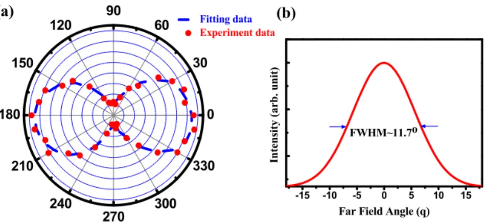
This high β value of our VCSEL could be responsible for low threshold operation of our laser. Fig. 10 shows the polarization characteristics and far-field pattern (FFP) of the laser emission. The laser emission has a degree of polarization of about 80% and the FWHM of the FFP is about 11.7° in both horizontal and vertical directions.
0 30 60 90 120 150 180 210 240 270 300 330 Fitting data Experiment data -15 -10 -5 0 5 10 15 In tensity ( ar b . unit)
Far Field Angle (q) FWHM~11.7o
(a) (b)
Fig. 10. (a) The polarization characteristics of the GaN VCSEL above the threshold. The experiment data is symbolized by red dots, and the blue dashed line is the fitting result. (b) Far field pattern of the laser spot at the threshold. The divergence angle was estimated to be around 11.7o.
CONCLUTION
We have analyzed the fabrication and development of GaN-based VCSELs from optical pumping to electrical pumping. We have fabricated a crack-free, high reflectivity AlN/GaN DBR by insertion of SL layers and using the high reflective Ta2O5/SiO2 as dielectric mirror to achieved laser operation under optical pumping at RT for the VCSELs with
hybrid DBR,. The optically pumped laser has a threshold energy at 55 nJ and a high degree of polarization of 89%, respectively. The higher spontaneous emission coupling factor of 6×10² is roughly estimated from the approximation
equations. Furthermore, based on the previous optically pumped hybrid VCSEL structures, we fabricated and demonstrated the first CW operation of an electrically pumped GaN-based VCSEL at 77K. The laser action occurred at a threshold current of 1.4 mA which has a dominated wavelength at 462.8 nm at 77 K. Furthermore, the laser has a low divergence angle of about 11.7 degree and a degree of polarization of among 80 %. The laser shows a strong spontaneous emission coupling with an estimated coupling efficiency of about 7.5×10². From the CCD image, a non uniform spatial
laser intensity emission image was also observed. Although the lasing action of electrically pumped GaN-based VCSEL has been observed at 77 K, there are still few technical issues and advanced structure design needed to be resolved. It is expected that the successful operation of electrically pumped GaN-based VCSELs at 77K is a useful and helpful guide for the design and fabrication of RT CW electrically pumped GaN-based VCSELs.
REFERENCES
[1] S. Nakamura, M. Senoh, and T. Mukai, “Highly p-typed Mg-doped GaN films grown with GaN buffer layers,” Jpn. J. Appl. Phys., 30, L1708–L1711 (1991).
[2] S. Nakamura, N. Iwasa, M. Senoh, and T. Mukai, “Hole compensation mechanism of p-type GaN films,” Jpn. J. Appl. Phys., 31, 1258–1266 (1992).
[3] K. Iga, “Surface-emitting laser-its birth and generation of new optoelectronics field,” IEEE J. Select. Topics Quantum Electron., 6(6), 1201–1215 (2000).
[4] W. W. Chow, K. D. Choquette, M. H. Crawford, K. L. Lear, and G. R. Hadley, “Design, fabrication, and performance of infrared and visible vertical-cavity surface-emitting lasers,” IEEE J. Quantum Electron., 33(10), 1810–1824 (1997).
[5] E. Towe, R. F. Leheny, and A. Yang, “A historical perspective of the development of the vertical-cavity surface-emitting laser,” IEEE J. Select. Topics Quantum Electron., 6(6), 1458–1464 (2000).
[6] H. Zhou, M. Diagne, E. Makarona, A. V. Nurmikko, J. Han, K. E. Waldrip, and J. J. Figiel, “Near ultraviolet optically pumped vertical cavity laser,” Electron. Lett., 36, 1777–1779 (2000).
[7] S.-H. Park, J. Kim, H. Jeon, T. Sakong, S.-N. Lee, S. Chae, Y. Park, C.-H. Jeong, G.-Y. Yeom, and Y.-H. Cho, “Room-temperature GaN vertical-cavity surface-emitting laser operation in an extended cavity scheme,” Appl. Phys. Lett., 83, 2121–2123 (2003).
[8] T. Tawara, H. Gotoh, T. Akasaka, N. Kobayashi, and T. Saitoh, “Low-threshold lasing of InGaN vertical-cavity surface-emitting lasers with dielectric distributed Bragg reflectors,” Appl. Phys. Lett., 83, 830–832 (2003).
[9] E. Feltin, G. Christmann, J. Dorsaz, A. Castiglia, J.-F. Carlin, R. Butté, N. Grandjean, S. Christopoulos, G. Baldassarri, H. von Högersthal, A. J. D. Grundy, P. G. Lagoudakis, and J. J. Baumberg, “Blue lasing at room temperature in an optically pumped lattice-matched AlInN/GaN VCSEL structure,” Electron. Lett., 43, 924–926 (2007).
[10] J.-T. Chu, T.-C. Lu, H.-H. Yao, C.-C. Kao, W.-D. Liang, J.-Y. Tsai, H.-C. Kuo, and S.-C. Wang, “Room-temperature operation of optically pumped blue-violet GaN-based vertical-cavity surface-emitting lasers fabricated by laser lift-off,” Jpn. J. Appl. Phys., 45, 2556–2560 (2006).
[11] J.-T. Chu, T.-C. Lu, M. You, B.-J. Su, C.-C. Kao, H.-C. Kuo, and S.-C. Wang, “Emission characteristics of optically pumped GaN-based vertical-cavity surface-emitting lasers,” Appl. Phys. Lett., 89, 121112 (2006).
[12] C.-C. Kao, Y. C. Peng, H. H. Yao, J. Y. Tsai, Y. H. Chang, J. T. Chu, H. W. Huang, T. T. Kao, T. C. Lu, H. C. Kuo, and S. C. Wang, “Fabrication and performance of blue GaN-based vertical-cavity surface emitting laser employing AlN/GaN and Ta2O5/SiO2 distributed Bragg reflector,” Appl. Phys. Lett., 87, 081105 (2005).
[13] C.-C. Kao, T. C. Lu, H. W. Huang, J. T. Chu, Y. C. Peng, H. H. Yao, J. Y. Tsai, T. T. Kao, H. C. Kuo, S. C. Wang, and C. F. Lin, “The lasing characteristics of GaN-based vertical-cavity surface-emitting laser with AlN-GaN and Ta2O5-SiO2 distributed Bragg reflectors,” IEEE Photon. Technol. Lett., 18(7), 877–879 (2006).
[14] S.-C. Wang, T.-C. Lu, C.-C. Kao, J.-T. Chu, G.-S. Huang, H.-C. Kuo, S.-W. Chen, T.-T. Kao, J.-R. Chen, and L.-F. Lin, “Optically pumped GaN-based vertical cavity surface emitting lasers: technology and characteristics,” Jpn. J. Appl. Phys., 46, 5397–5407 (2007).
[15] T-C. Lu, C.-C. Kuo, H.-C. Kuo, G.-S. Huang, and S.-C. Wang, “CW lasing of current injection blue GaN-based vertical cavity surface emitting laser,” Appl. Phys. Lett., 92, 141102 (2008).
[16] F. A. Ponce and D. P. Bour, “Nitride-based semiconductors for blue and green light-emitting devices,” Nature, 386, 351–359 (1997).
[17] X. H. Zhang, S. J. Chua, W. Liu, L. S. Wang, A. M. Yong, and S. Y. Chow, “Crack-free fully epitaxial nitride microcavity with AlGaN/GaN distributed Bragg reflectors and InGaN/GaN quantum wells,” Appl. Phys. Lett., 88, 191111 (2006).
[18] H. Benisty, H. De Neve, and C. Weisbuch, “Impact of planar microcavity effects on light extraction-part I: basic concepts and analytical trends,” IEEE J. Quantum Electron., 34(9), 1612–1631 (1998).
[19] H. Benisty, H. De Neve, and C. Weisbuch, “Impact of planar microcavity effects on light extraction-part II: selected exact simulations and role of photon recycling,” IEEE J. Quantum Electron., 34(9), 1632–1643 (1998).
[20] R. J. Horowicz, H. Heitmann, Y. Kadota, and Y. Yamamoto, “GaAs microcavity quantum-well laser with enhanced coupling of spontaneous emission to the lasing mode,” Appl. Phys. Lett., 61, 393–395 (1992).
[21] Y. Yamamoto and S. Machida, “Microcavity semiconductor laser with enhanced spontaneous emission,” Phys. Rev. A., 44, 657–668 (1991).
[22] S. Kako, T. Someya, and Y. Arakawa, “Observation of enhanced spontaneous emission coupling factor in nitride-based vertical-cavity surface-emitting laser,” Appl. Phys. Lett., 80, 722–724 (2002).
[23] A. Kaneta, K. Okamoto, Y. Kawakami, S. Fujita, G. Marutsuki, Y. Narukawa, and T. Mukai, “Spatial and temporal luminescence dynamics in an InxGa1−xN single quantum well probed by near-field optical microscopy,” Appl. Phys.
Lett., 81, 4353–4355 (2002).
[24] B. Witzigmann, V. Laino, M. Luisier, U. T. Schwarz, G. Feicht, W. Wegscheider, K. Engl, M. Furitsch, A. Leber, A. Lee, and V. Härle, “Microscopic analysis of optical gain in InGaN/GaN quantum wells,” Appl. Phys. Lett., 88, 021104 (2006).