Threshold gain analysis in GaN-based photonic
crystal surface emitting lasers
Peng-Hsiang Weng, Tzeng-Tsong Wu, Tien-Chang Lu,* and Shing-Chung Wang
Department of Photonics & Institute of Electro-Optical Engineering, National Chiao Tung University, Hsinchu 30050, Taiwan *Corresponding author: [email protected]
Received March 8, 2011; revised April 20, 2011; accepted April 20, 2011; posted April 21, 2011 (Doc. ID 143484); published May 13, 2011
We have analyzed threshold gains and lasing modes in GaN-based photonic crystal (PC) surface emitting lasers (PCSELs) by using the multiple scattering method (MSM) for triangular-lattice PC patterns. Moreover, GaN-based PCSELs with different boundary shapes have been fabricated and measured. The lasing mode at theΓ band edge of GaN-based PCSELs can be identified by using the angled resolved spectroscopy and matched well to the results calculated by MSM. Threshold conditions in the GaN-based PCSELs with different boundary shapes are obtained by optical pumping and agree well with simulation results. © 2011 Optical Society of America
OCIS codes: 140.5960, 140.7270, 160.5298.
Photonic crystal (PC) surface emitting lasers (PCSELs) utilizing two-dimensional (2D) distributed feedback me-chanisms have attracted much attention and have been widely researched during the past decade [1–7]. PCSELs have many advantageous characteristics, such as single-mode operation in a large lasing area, a symmetric beam shape, and a low divergence angle. With these superior properties, PCSELs can be applied to high-density optical storages, laser printers, and micro- or picoprojectors. Numerical studies have attempted to explain the distrib-uted feedback mechanism for PCSELs by using different theoretical methods. Sakoda et al. used group-velocity anomaly to evaluate lasing threshold by the plane wave expansion method (PWEM) [8]. Lee et al. investigated the
quality factor near band edges of finite-size PCs by the finite-difference time-domain (FDTD) method [9]. Sakai et al. calculated the coupling coefficients for triangular PCs and the threshold gain at the frequency deviated from the Bragg frequency for square PCs both by using the couple wave theory [10,11]. Nojima proposed the multiple scattering method (MSM) to calculate lasing be-haviors in PC lattice atoms with optical gains [12]. There are different advantages and limitations while using these theoretical methods to calculate characteristics of PC la-sers. For example, the 2D PWEM better applies to the infinite PC structure, which is usually not the case for actual devices. FDTD method consumes numerous com-puter resources and calculation time to simulate the fi-nite domain structure. On the contrary, the MSM has many advantages, such as less calculation time, capabil-ity in considering real optical gain in material, and more accurate solutions. Therefore, the purpose of this Letter is to investigate the threshold gain properties of GaN-based PCSELs at theΓ band edge with triangular-lattice patterns using the MSM and compare simulation results with experimental data.
The structure for simulation is composed of finite two dimensional PCs with triangular-lattice patterns made by parallel cylinders placed in a uniform GaN-based back-ground material. Here, the complex dielectric constant is introduced to describe the light amplification in the background material. The dielectric constant can be written as
εbackgoundðωÞ ¼ εGaNðωÞ − i
2cpffiffiffiffiffiffiffiffiffiεGaN
ω k00a; ð1Þ
where εGaN is the dielectric constant varied with
fre-quency of light and ka00is the amplitude gain coefficient
of the material. A point source transmitted monochro-matic waves is placed at the origin point. The total system matrix can be obtained as [12]
Γi nAin− XN j¼1;j≠i X∞ l¼−∞ Gi;jl;nAjl¼ Ti n: ð2Þ
The Ani and Tni are matrixes representing expansion
coefficients of scattering waves and incident waves, re-spectively. Here, we only consider the TE mode polariza-tion (polarizapolariza-tion direcpolariza-tion perpendicular to the cylinder axis) according to main dipole oscillating direction in our GaN active region [13]. Equation (2) could be simplified to an eigenvalue problem: MA¼ T. If the value of vector A=T is divergent, the laser oscillation condition would be thus achieved. Therefore, detðMÞ ¼ 0 is the complex de-terminant equation used to search for a pair of variables of threshold amplitude gain kam00 and normalized
fre-quency from k ¼ ω=c in Eq. (1).
Figure1(a)shows photonic band dispersion curves of a triangle lattice PC with TE mode polarization calcu-lated by PWEM near the firstΓ band edge. The structural parameters for the calculation are similar to our previous reports [13]. Four different band edges can be found re-sulting in four resonant modes (A − D), while modes B
Fig. 1. (Color online) (a) Photonic band dispersion curves of a triangle lattice PC with TE mode polarization calculated by PWEM near the first Γ band edges showing four different modes. (b) Normalized frequencies of lasing modes calculated by the MSM for different PC shells (N values).
1908 OPTICS LETTERS / Vol. 36, No. 10 / May 15, 2011
and D are doubly degenerate. Figure1(b)shows the nor-malized frequencies of lasing modes calculated by the MSM for different PC shells (N values). Here, a size pa-rameter N is introduced to represent the number of cy-linder layers in theΓ − M direction. The resonant mode frequencies near band edges are calculated as a function of the shell number of PCs. The dashed lines in Fig. 1
represent different resonant modes A, B, C, and D at the Γ band edge. It can be observed that the resonant mode frequencies calculated by the MSM will approach the band edge frequencies as the shell number increases. Therefore, we could obtain more accurate results when the layer number is beyond 20. The blueshifted or red-shifted trends of normalized frequencies as the shell number increases in Fig. 1(b) are due to the shapes of photonic band curves. For example, the downward curve of mode B and the upward curve of mode C near the Γ point in Fig.1(a)would result in the redshifted and blue-shifted trends of normalized frequencies in Fig. 1(b), respectively.
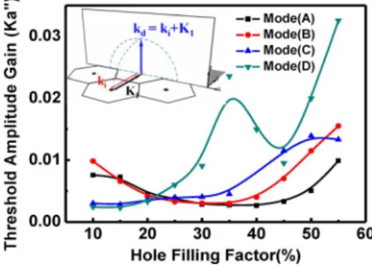
As shown in Fig. 2, the threshold amplitude gain of modes A − D is calculated as a function of the hole-filling factor by the MSM. The confinement factor and effective refractive index of 0.865 and 2.482 for guided modes were used in the calculation. Hence, real parts of εGaN
and εHole are 7.487 and 3.065 for the matrix material
and PC holes [13,14]. In the inset in Fig.2, the blue arrow kdmeans the major output direction of light is normal to
the PC plane using Bragg diffraction scheme [7]. Further-more, the threshold gain of four resonant modes is varied with the filling factor. Among all the resonant modes, modes A and B have the lowest threshold gain for hole-filling factors of 35% and 30%, while mode C and D have the lowest threshold gain for hole-filling factors of 10% and 15%. This result shows that the hole-filling factor controls the mode selection scheme. The proper hole-filling factor can be selected to fabricate PCSELs operated in a specific mode.
Then, PCSELs with two different boundary shapes are fabricated to compare threshold gain characteristics. Scanning electron microscope (SEM) images in Fig. 3
show different boundary shapes of PCSELs; one is a cir-cular shape and the other is a hexagonal shape. The laser structure was grown with a 2 μm GaN buffer layer, a 25-pair GaN/AlN distributed Bragg reflector (DBRs), a 675-nm-thick n-GaN layer, 10 pairs of InGaN/GaN
multiple quantum wells, a 24-nm-thick AlGaN p-cladding layer, and a 115-nm-thick p-GaN layer by metal organic chemical vapor deposition on a 2 in: c plane sapphire sub-strate. The gain peak of multiple quantum wells was about 408 nm with a linewidth of about 10 nm, depending on the pumping intensity. The electron-beam lithography was used to define the pattern of PCs with the triangle lattice on the sample surface. Diameters of both PC re-gions are about 50 μm. The lattice constant a is 190 nm, and the r=a ratio is 0.3, where r is the radius of a PC hole. Then, the PC pattern was etched about 400 nm down to n-GaN by using the inductively coupled plasma system. The detailed growth conditions and fabrication process can be found elsewhere [7].
A 325 nm cw He–Cd laser and a 355 nm YVO4 pulse
laser are used as optical pumping sources in the angle-resolved photoluminescence (ARPL) system [13]. Figure 4 shows pumping results by using the ARPL system. Figures 4(a) and 4(b) were obtained by using the He–Cd pumping laser and the pulse laser, respec-tively. The red dashed curves in Fig. 4 represent the photonic band dispersion curves as shown in Fig. 1(a)
and matched well to the measured diffracted curves. The multiple diffracted curves result from several in-plane guided modes in the laser structure and the black dashed lines represent the slope of diffracted curves. On the other hand, the smile-shape curves in ARPL diagrams re-sult from vertical Fabry–Perot modes in our laser struc-ture. In Fig.4(b), the lasing point of PCSELs is matched to the mode B of the band diagram at the Γ band edge. According to the calculated result of mode A − D in Fig.2, modes A and B show lower threshold gain than modes C and D when the filling factor is around 0.3. This result shows a good agreement with the lasing characteristic pumped by the ARPL system. The reason mode A was not observed was due to the large offset between the mode A and the gain peak in the active layers.
Moreover, the threshold of circular boundary and hexagonal boundary PCSELs pumped by the 355 nm
Fig. 2. (Color online) Threshold amplitude gain of four modes as a function of the hole-filling factor. The inset shows the lasing mode at Γ point in the PC plane using the Bragg diffraction scheme [7].
Fig. 3. SEM images of the (a) circular boundary and the (b) hexagonal boundary PC patterns of a GaN-based PCSEL.
Fig. 4. (Color online) Measured ARPL diagrams near the Γ point. The red dashed lines represent the calculated photonic band dispersion curves. ARPL diagrams pumped by an (a) He–Cd laser and a (b) YVO4pulse laser.
YVO4 pulse laser is shown in Fig.5. The pumping spot size of the YVO4 laser is estimated to be about 50 μm in diameter. The lasing wavelengths for the hexagonal boundary and the circular boundary are 406 and 403 nm. The lasing linewidths for the hexagonal boundary and the circular boundary are 0.28 and 0:25 nm, respectively. Pumping energy densities for the circular boundary and the hexagonal boundary PCSELs are 2.8 and 3:1 mJ=cm2, respectively. The threshold amplitude gains
of the circular boundary and the hexagonal boundary PCSELs are also simulated with the same parameters by the MSM to be 2:784 × 10−3 and 3:798 × 10−3, respec-tively. Based on simulation results and experiments, the PCSEL with the circular boundary shows lower thresh-old than that with the hexagonal boundary. The reason could be because the circular boundary provides more symmetric reflection in the PC structure. The experimen-tal results are consistent with simulation results, demon-strating that the MSM can be used as a fast and cost effective designing tool for PCSEL structures.
In conclusion, we have constructed MSMs to calculate the normalized frequency and threshold gain versus PC shell numbers, different filling factors, and different boundary conditions of GaN-based PCSELs with triangu-lar-lattice patterns. The A, B, C, and D modes have their lowest threshold gain for filling factors of 35%, 30%, 10%, and 15%, respectively. It is demonstrated that proper de-sign of the hole-filling factor can be selected to fabricate PCSELs operated in a specific mode.
Furthermore, GaN-based PCSELs with different boundary shapes are fabricated and measured. From ARPL results, the lasing mode can be identified as mode B at the Γ band edge, which is predicted by the simula-tion. Finally, the threshold energy densities of the circu-lar boundary and the hexagonal boundary under the optical pumping condition are about 2.8 and 3:1 mJ=cm2,
which shows good agreement with the simulation result. We believe the presented results will be beneficial to the fast design and development for PCSEL devices covering different semiconductor materials, such as GaAs, InP, and ZnO, in the near future.
The authors would like to gratefully acknowledge P. G. Luan at National Central University (NCU) for his fruitful suggestions. This work was supported in part by the Ministry of Education Aim for the Top University pro-gram and in part by the National Science Council of Taiwan (NSCT) under contract NSC 98-3114-M-009-001.
References
1. M. Meier, A. Mekis, A. Dodabalapur, A. Timko, R. E. Slusher, J. D. Joannopoulos, and O. Nalamasu, Appl. Phys. Lett.74, 7 (1999).
2. M. Imada, A. Chutinan, S. Noda, and M. Mochizuki, Phys. Rev. B65, 195306 (2002).
3. I. Vurgaftman and J. Meyer, IEEE J. Quantum Electron.39, 689 (2003).
4. D. Ohnishi, T. Okano, M. Imada, and S. Noda, Opt. Express 12, 1562 (2004).
5. M. Kim, C. S. Kim, W. W. Bewley, J. R. Lindle, C. L. Canedy, I. Vurgaftman, and J. R. Meyer, Appl. Phys. Lett. 88, 191105 (2006).
6. H. Matsubara, S. Yoshimoto, H. Saito, Y. Jianglin, Y. Tanaka, and S. Noda, Science319, 445 (2008).
7. T. C. Lu, S. W. Chen, L. F. Lin, T. T. Kao, C. C. Kao, P. Yu, H. C. Kuo, S. C. Wang, and S. H. Fan, Appl. Phys. Lett.92, 011129 (2008).
8. K. Sakoda, K. Ohtaka, and T. Ueta, Opt. Express 4, 481 (1999).
9. Y. H. Lee, H. Y. Ryu, and M. Notomi, Phys. Rev. B 68, 045209 (2003).
10. K. Sakai, J. Yue, and S. Noda, Opt. Express16, 6033 (2008). 11. K. Sakai, E. Miyai, and S. Noda, IEEE J. Quantum Electron.
46, 788 (2010).
12. S. Nojima, J. Appl. Phys.98, 043102 (2005).
13. S. W. Chen, T. C. Lu, Y. J. Hou, T. C. Liu, H. C. Kuo, and S. C. Wang, Appl. Phys. Lett.96, 071108 (2010).
14. Y. Y. Chen and Z. Ye, Phys. Rev. E65, 056612 (2002). Fig. 5. (Color online) Measured output intensity versus input
excitation energy density of GaN-based PCSELs with bottom AlN/GaN distributed Bragg reflectors. The black solid squares and red solid circles represent the circular boundary and the hexagonal boundary, respectively.