國 立 交 通 大 學
電子工程學系 電子研究所碩士班
碩 士 論 文
運用隨機電報訊號方法分析
三閘極電晶體的多層級氧化層陷阱
The Multi-trap Analysis of Trigate MOSFETs Using the
Random Telegraph Noise Measurement
研 究 生 :蔡侑璉
指導教授 :莊紹勳 博士
二氧化鉿電阻式記憶體多位元操作之
隨機電報雜訊分析
The Random Telegraph Noise (RTN) Analysis of
Multi-Level Operation Methods in HfO
2-based Resistive
Random Access Memory
研 究 生 : 蔡侑璉 Student : You-Lian Tsai
指導教授 : 莊紹勳 博士 Advisor : Dr. Steve S. Chung
國立交通大學
電子工程學系 電子研究所碩士班
碩士論文
A Thesis
Submitted to Department of Electronics Engineering and
Institute of Electronics
College of Electrical and Computer Engineering
National Chiao Tung University
In Partial Fulfillment of the Requirements
for the Degree of
Master of Science
in
Electronics Engineering
November 2012
Hsinchu, Taiwan, Republic of China.
i
運用隨機電報訊號方法分析
三閘極電晶體的多層級氧化層陷阱
學生:蔡侑璉 指導教授:莊紹勳 博士
國立交通大學
電子工程學系 電子研究所碩士班
摘要
隨著互補式金氧半電晶體(CMOS)的微縮,隨機電報訊號對元件產生劇烈的汲極電流 波動所造成的影響是極為重要的可靠度議題之一。 隨機電報訊號的產生是由於單一載 子從基板穿隧至閘極氧化層而被捕捉的物理現象。在本篇論文中,我們可以觀察此種缺 陷的物理特性,且利用改良的萃取方法去準確得知缺陷的能階以及深度。 隨著超大型積體電路微縮至22奈米,漏電問題以及大幅的變異(variation)擾動問題, 使得傳統的平面電晶體將不敷未來微縮用途,因此,在1999年所提出的三閘極電晶體 (trigate) 結構在近幾年受到進一步的重視。然而在這樣的新型結構中依然存在著許多問 題尚待解決,根據我們的觀察隨機電報訊號就是其中一項導致變異的重要來源。本文 中,我們發表的一種簡單的實驗方法來萃取隨機電報訊號缺陷在互補式金氧半電晶體通 道方向和氧化層中深度的分佈位置。為了研究隨機電報訊號對三閘極電晶體的影響,我 們採用平面電晶體來和三閘極電晶體做比較。由實驗結果得知,在製流中產生的隨機電 報雜訊缺陷在不同結構的元件中分佈特性並不相同,亦即在三閘極電晶體中缺陷分佈位 置較靠近多晶矽閘極,而在平面電晶體中缺陷位置卻較為靠近基板。此外我們發現造成 多層級隨機電報訊號的原因,這是由於氧化層中兩個缺陷的位置過於接近,以至於缺陷 能帶的分佈互相重疊所導致。ii
根據上述單一元件中多層級隨機電報雜訊的研究,我們將它運用於對於靜態隨機記 憶體(SRAM, Static Random Access Memory)的影響。利用隨機電報雜訊造成門檻電壓 的擾動原理,我們可以成功的解釋靜態隨機儲存器在蝴蝶圖轉換的過程中發生錯誤的機 制。此外,我們由蝴蝶圖中萃取出讀取靜態雜訊邊際,並比較隨機電報訊號的產生對讀 取靜態雜訊邊際的影響,在此情況下此我們觀察到隨機電報訊號將會造成讀取靜態雜訊 邊際擾動,擾動範圍可由2mV至23mV。在量測中我們明顯發現蝴蝶圖受到隨機電報訊 號的影響而分裂,分裂開來的層級數正好相當於多層級隨機電報訊號的層級數。此一現 象將是未來使用三閘極電晶體來設計SRAM時,必需謹慎考量的一項重要微縮因素。
iii
The Multi-trap Analysis of Trigate MOSFETs Using the
Random Telegraph Noise Measurement
Student:Yu-Lien Tsai
Advisor:Dr. Steve S. Chung
Department of Electronics Engineering
Institute of Electronics
National Chiao Tung University
Abstract
As CMOS devices are continuously scaled, the influence of Random Telegraph Noise (RTN) in CMOS devices is one of the most important reliability issues. The RTN phenomena are resulted from the single carrier trapped and de-trapped between the channel and the trap in the gate dielectrics. In this thesis, we have observed the physical properties of single trapped carriers through a novel RTN profiling technique. This technique enables the extraction of the lateral location and vertical depth of a single trap or multiple traps in an advanced trigate nMOSFET device.
As VLSI technology scaled toward 22nm node, the short channel effect and variability are intolerant in the planar architecture. So, even FINFET structure has been proposed since 1999 which received much more attention more recently. However, there are several problems which need to be solved in such a device. According to our observation, RTN is one of the most important variation sources. In this thesis we develop a simple experiment method to extract the two dimensional distribution of RTN traps. To study the influence on trigate MOSFETs, we compare
iv
trigate devices with conventional planar devices. From the profiling results, we have found that the process-induced RTN traps are generated near poly gate in trigate devices but generated near the channel of the planar devices. In addition, we have found the origins of multi-level RTN generation, which came from the cross-section of overlap traps.
Based on the results of our research of RTN at the device-level, we further investigate the impact of multiple RTN on SRAM and find a newly RTN-induced failure mechanism of SRAM successfully. Besides, we extract the RSNM from butterfly curves. Comparing the RSNM (read static noise margin) of the cell with RTN and without RTN respectively, the RSNM has been degraded from 2mV to 23mV in this work because of multi-RTN. From the measurement, butterfly curves are split into multiple levels, which is corresponding to the multiple levels of RTN in a pull-down or pull-up device directly. These phenomena are first reported and will be significant for consideration in the future design of trigate SRAM.
v
致 謝
兩年的研究生生涯一轉眼就過去了,還記得剛考上研究所,來到
人生地不熟的新竹,面對課業上新的挑戰,心中滿是不安,因此我
要特別感謝在這兩年之中,不論是研究上、課業上、生活上給予我
幫助的每一個人。首先要向我的指導教授莊紹勳老師表達深摯的謝
意。老師在課業和研究中給予我們寶貴的指導與建議,讓我在學業
與研究上獲益良多,更讓我們學習到對事物應有的嚴謹態度。
此外我要感謝實驗室所有一起努力的學長和夥伴,感謝周承翰、
謝易叡學長,在我對實驗一無所知的時候是你們將那寶貴的知識傳
承了下來,謝易叡學長謝謝你耐心地帶領我做實驗,讓我能快速地
進入狀況,以及一起努力的同學蔡漢旻、黃英傑、蔡政達、謝泓達、
房定樺,和你們一起討論,讓我在遇到瓶頸的時候能夠有新的靈感,
遇到挫折的時候有堅持下去的力量,有你們的陪伴讓黯淡的實驗室
更加添了一抹色彩,另外還有汪大暉老師實驗室的學長們,邱榮標、
鍾岳庭、周佑亮學長,感謝你們在我實驗遭遇困難而停擺的時候,
向你們請教時不吝給我意見,真的助益量多。最後還有實驗室的學
弟,伍邦齊、林尚墩、陳敬翰、王漢樽、林宗慶,衷心的期盼你們
vi
在將來的日子裡都能夠互相扶持,在困境中彼此幫忙,也預祝你們
學業、實驗盡都順利,也祝你們都能如期畢業。
最後我要感謝那些為我加油,使我能夠有信心面對挑戰的家人以
及朋友,你們在我軟弱的時候給我力量,為我禱告,這一路上謝謝
你們的陪伴,最後我要感謝上帝,祢是我心中的磐石;我必不致缺
乏,感謝祢成為我腳前的燈路上的光,引領我每個步伐,謹將這份
榮耀歸給我天上的父。
2012 年 11 月下旬
vii
Contents
Chinese Abstract
……….………… i
English Abstract
……….………… iii
Acknowledgements ……….………… v
Contents
……….………… vii
Figure Captions
……….………… ix
Chapter 1 Introduction
1
1.1 Background ………... 1
1.2 The Motivation of this Work ……… 3
1.3 Organization of This Thesis ……….. 4
Chapter 2 Theory of Profiling Method and Experiment Setup
10
2.1 Introduction ………... 10
2.2 Profiling Method in Two Dimension ……… 11
2.2.1 General Equation of the Trap Depth ……… 11
2.2.2 Lateral Profiling Method ……….. 13
2.3 Device Preparation and Experimental Setup ……… 14
2.3.1 Device preparation ………... 14
viii
Chapter 3 Influence of Multi-level RTN in Trigate MOSFET And
the Distribution of Oxide Trap Through 2-D Profiling
25
3.1 Introduction ……….……….. 25
3.2 Experimental ………. 26
3.2.1 Process Induce RTN Trap ……… 26
3.2.2 Stress Induce RTN Trap ……….……….. 29
Chapter 4 The Applications of Multi-RTN: The Impact on SRAM
Operation & The Manipulation of RTN-trap Positions
47
4.1 Introduction ……….……….. 474.2 The Basics of SRAM………. 49
4.2.1SRAM Operations ……….………... 49
4.2.2 Steady Noise Margin ……….………... 50
4.2.3 Impact of Multi-level RTN on SRAM ………. 51
4.3 The Manipulation of RTN-trap Positions ………. 52
Chapter 5 Summary and Conclusion
74
References
………76
ix
Figure Captions
Chapter 1
Fig. 1.1 (a) Carrier trapping and drameter of the RTN noise: capture time τc,
emission time τe, and current amplitude ΔID. 6
Fig. 1.2 The schematic diagram of Multi-level RTN. 7
Fig. 1.3 A Two-level RTN schematic diagram. 8
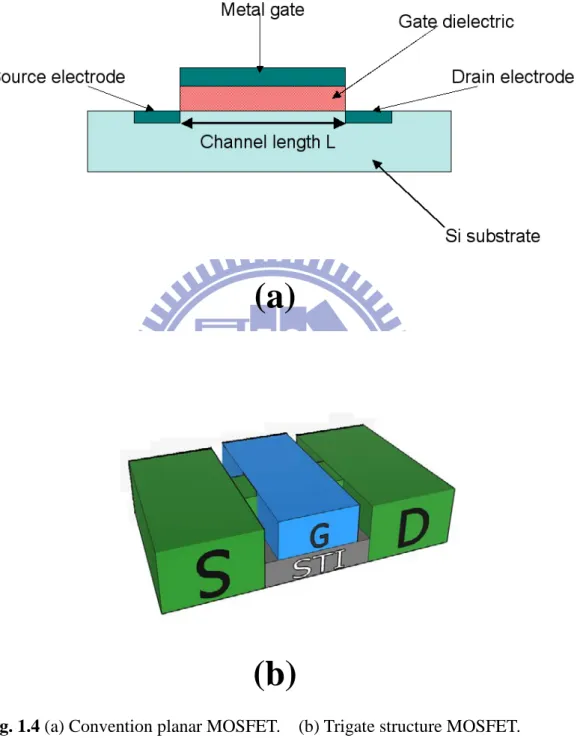
Fig. 1.4 (a) Conventional planar MOSFET. (b) Trigate structure MOSFET. 9
Chapter 2
Fig. 2.1 (a) Illustration of the three parameter of the RTN noise: capture time
τc, emission time τe, and current amplitude ΔID. (b) Carrier trapping and detrapping by the slow trap near the drain side. 16
Fig. 2.2 The energy band diagram of the Si-SiO2 interface in the channel at
the trap location. 17
Fig. 2.3 Oxide trap RTN induced barrier peak fluctuatuation: Vth variation is
dominated by the trapping or de-trapping in the oxide layer trap. 18
Fig. 2.4 A new model is to approximate the carrier peak in the channel as a second degree curve, in which the peak position can be determined
by the DIBL. 19
Fig. 2.5 (a) The 3D schematic of bulk trigate device used in this work. (b) The cross-section from Y to Y+ of trigate device. 20
x
Fig. 2.7 The experimental system of current-voltage (I-V) for both n-type or p-type MOSFET. 22
Fig. 2.8 The measurement setup using Analyzer HP 4156C to do the sampling of RTN signals. 23
Fig. 2.9 The terminals setup for the sampling using HP4156C Analyzer. 24
Chapter 3
Fig. 3.1 The profiling result of the process-induced single RTN in the bulk planar pMOS devices, showing a Gaussian-like profile. The insert is the ΔId/Id data of this RTN, confirming that there is only single RTN
trap. 32
Fig. 3.2 The profiling result of process-induced multi-RTN in the bulk planar nMOS devices, showing 2 Gaussian-like packets, traps b & c. Note that we categorize this result into the Cases 1, 2, and 3. For the Case 2, two packets are overlapped in tails. 33
Fig. 3.3 ∆Id/Id data of RTN for three cases in Fig.3.2. For Case 1, two levels
are observed, induced by trap b without the interference from trap c. Case 3 is the opposite case to the Case 1. But, Case 2 shows 4 level ΔId/Id data, which comes from the interaction between the traps b &
c. 34
Fig. 3.4 The result of the profiling of the process-induced single-RTN in the bulk trigate pMOS devices, showing a Gaussian-like distribution. 35
Fig. 3.5 The result of the profiling of the process-induced two-RTN traps in the bulk trigate nMOS devices, showing 2 Gaussian-like waveforms, but both waveforms are not overlapped because of a large distance 36
xi
between them.
Fig. 3.6 (left) the ln(τc/τe) dependency of the bulk planar pMOS devices,
showing the positive dependency, but (right) the bulk trigate devices shows the negative dependency. 37
Fig. 3.7 From judging the RTN proofing data and ln(τc/τe) dependency, we
conclude that (up) RTN of planar devices are near the interface between the oxide and Si; (down) RTN of trigate devices are near the interface between the oxide and poly-Si. 38
Fig. 3.8 Summary the information of process induced RTN in this work. 39
Fig. 3.9 The comparisons of the cross-section of the process-induced RTNs in this work. The reported data and the theoretical value show good
consistency. 40
Fig. 3.10 The result of the HC stresss-induced multi-RTN in bulk planar nMOS devices, showing 2 Gaussian-like packets, traps g & h with strong interference. We categorize this result into the Case 1, 2, and 3. For the Case 2, two packets are overlapped in tails. 41
Fig. 3.11 Cases 1, 2, & 3 addressed in Fig. 3.10. Case 1 shows clear 2 level of ΔId/Id for trap-g induced RTN, and the Case 3 is the same for trap-h.
But the Case 2 shows 4-level behavior composed by the trap-g & trap-h. Lvs.1 &2 are contributed from the trap-h, the others are from
the trap-g. 42
Fig. 3.12 The result of the NBTI stress-induced single-RTN in the bulk planar pMOS devices, showing a Gaussian-like shape. Note that this shape distributes near the middle of the channel region. 43
xii
Fig. 3.13 The result of the HC stress-induced single-RTN trap in bulk trigate nMOS devices, showing a bell shape. Note that this shape distributes near the region of drain side. 44
Fig. 3.14 The result of the NBTI stress-induced 2-RTN traps in bulk trigate nMOS devices. These two traps are totally overlapped in the shape and aligned on the same channel position with very close trap depths. 45
Fig. 3.15 (a) The 3 level RTN was observed in the Case 1 addressed in Fig.
3.14. There is no Lv.4, which two traps are overlapped. This is due to the fact that Coulomb repulsive force of a trapped trap rejects the trapping process of empty traps, (b) & (c). 46
Chapter 4
Fig. 4.1 The schematic of SRAM cell. The SRAM cell consists of a bistable flip-flop connected to the internal circuitry by two access transistors. 54
Fig. 4.2 Read/write operations. 55
Fig. 4.3 (Top) The schematic of the SRAM circuit. (Bottom) The TEM view
of SRAM. 56
Fig. 4.4 Two multi-RTN cases utilized to study the impact of multi RTN on
SRAM. 57
Fig. 4.5 The butterfly curves of planar SRAM with multi-RTN in M2 device.
Note that the branch (red) with RTN traps has more fluctuation than that without RTN trap (blue) one. The insert is the zooming up, in which clear 4 level characteristic is observed, corresponding to 4 level Id RTNof M2 devices. 58
xiii
Fig. 4.7 The butterfly curves of trigate SRAM with multi-RTN in M2 device. Note that the branch (red) with RTN traps has more fluctuation than that without RTN trap(blue) one. 60
Fig. 4.8 Clear 4 levels characteristic is observed, corresponding to 4 level Id
RTNof M2 devices. 61
Fig. 4.9 As a result of multi-RTN in the oxide of M2 devices, the variation of RSNM will increase astonishingly. Note that the variation of RSNM increases much larger in trigate devices than that of planar devices. 62
Fig. 4.10 The butterfly curves of planar SRAM with multi-RTN in M2 & M3 device. Note that the red branch shows transition failure component (the insert) due to multi-RTN in M3&M2 devices. This is a newly RTN induced SRAM failure mechanism. 63
Fig. 4.11 The butterfly curves of trigate SRAM with multi-RTN in M2 & M3 devices. Note that the red branch shows transition failure component (the insert) due to multi-RTN in M3&M2 devices. This is a newly RTN induced SRAM failure mechanism. 64
Fig. 4.12 The schematic to explain why multi-level transition and failure of transition in butterfly curves of SRAM. The RTN-induced Vt shift in M2 or M3 causes these abnormal transitions of curves. 65
Fig. 4.13 The schematic to indicate that vertical electric field is approach to horizontal electric field, therefore RTN-traps in this stress condition is near the drain side. 66
Fig. 4.14 The result of the HC stress-induced single-RTN trap in bulk planar nMOS devices, showing a bell shape. Note that this shape distributes 67
xiv
near the drain side.
Fig. 4.15 The schematic to indicate that vertical electric field is approach to the horizontal electric field, therefore RTN-traps in this stress condition is near the drain side. 68
Fig. 4.16 The result of the HC stress-induced single-RTN trap in bulk planar nMOS devices, showing a bell shape. Note that this shape distributes more far from the drain side region. 69
Fig. 4.17 The result of IB and IB /ID versus VG curve at different VD for hot
carrier stress condition. 70
Fig. 4.18 The schematic to indicate the uniform distribution of electric field, therefore RTN-traps in this stress condition distribute uniformly in
the channel. 71
Fig. 4.19 The result of the FN stress-induced double-RTN traps in bulk planar nMOS devices, showing a bell shape. Note that this shape distributes more in the center of drain side. 72
Fig. 4.20 The ln(τc/τe) dependency of the profiling result, (left) showing the positive dependency for left traps, but (right) the right traps shows the negative dependency. 73
1
Chapter 1
Introduction
1.1 Background
Silicon CMOS has been the main stream IC fabrication technology for three decades. In the last few years, the industry has witnessed a striking progress in downsizing the planar CMOS. Despite many fabrication challenges, 15nm physical gate length bulk MOSFETs have been demonstrated. However, scaling planar CMOS to 10nm-and-below would be exceptionally difficult, if not completely impossible, due to electrostatics, excessive leakages, mobility degradation, and many realistic fabrication issues. Particularly, the control of leakage (hence power) in a nanoscale transistor would be critical to high- performance chips such as microprocessors. Non-planar MOSFETs provide potential advantages in packing density, carrier transport, and device scalability. FinFET structure MOSFETs have been researched for a decade [1.1], they were not seriously considered by the industry due to their complicated fabrication process. These structures have regained attentions in deep-sub-100nm CMOS due to many scaling limits associated with the planar CMOS.
FinFET devices are suitable in sub-32 nm technology owing to their superior short channel control, steep subthreshold swing, and immunity to Random Dopant Fluctuation
2
(RDF) [1.2] with lightly-doped or undoped silicon fins. However, in extremely scaled devices, the impacts of RTN [1.3-1.4] resulting from trapping/detrapping of a single carrier charge in defect state at the interface have become serious concerns in deca-nanometer MOSFETs. Furthermore, the RTN amplitude exhibits long-tailed distribution and inverse area dependency. Thus, RTN has created a serious variation source in BULK MOSFETs as well as thin silicon film based multi-gate devices. In this work, we evaluate the effect of multi-charged trap induced RTN on the analog properties of FinFET and Bulk-planar devices by 2-D profiling method.
On the other hand, the soft error susceptibility of SRAMs has significantly increased in the nanometer regime. In recent years, the variations of devices have induced circuit failed, and it is an important issue that should be solved immediately [1.5-1.7]. RTN is one of the most important variation issues, especially multiple RTN.
In this thesis, the generation mechanism of RTN traps has been found. Instead of charge pumping method [1.8], we proposed a new method to profile the distribution of multi-RTN traps, because the charge-pumping current may be too small to be reliably measured in small-size devices at a lower frequency required. Using the method we proposed in this thesis a newly RTN-induced failure mechanism of trigate SRAM was found, and it will be very valuable in the future reliability and technology of SRAM cell.
3
1.2 The Motivation of this Work
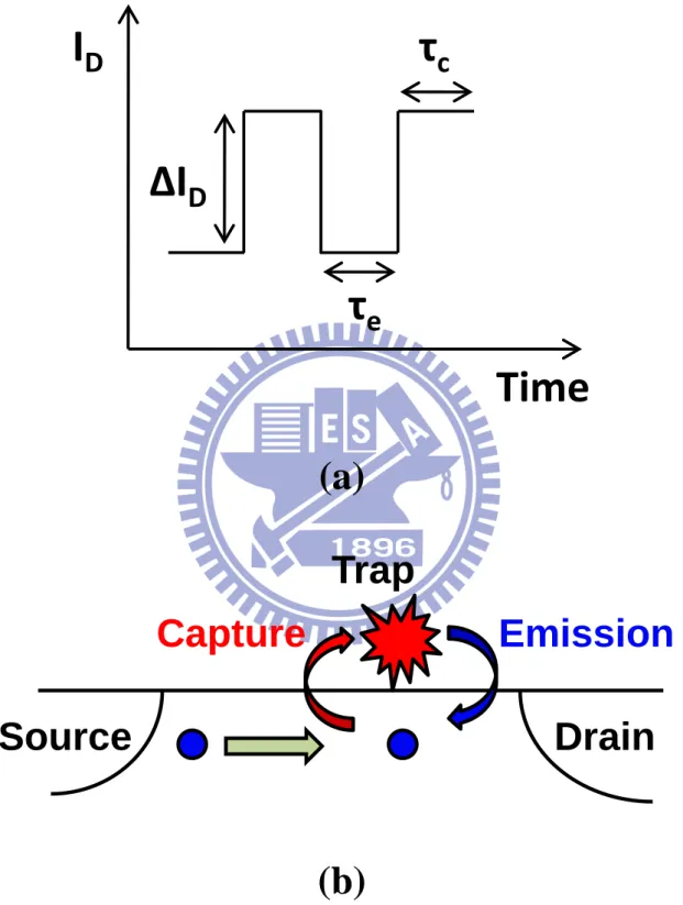
Recently, random telegraph noise has been regarded as a serious concern for CMOS device scaling. It is caused by the capture and emission of charge carriers in the gate oxide traps and results in severe Id fluctuation as shown in Fig. 1.1 (a), and threshold
voltage shift as shown in Fig. 1.1 (b). Due to its strong dependence on device dimension, it is predicted that RTN amplitude will grow with device scaling more rapidly than that the Vth variation caused by random dopant fluctuation. Therefore, new methods for measuring
and modeling RTN are necessary to gain more understanding of the statistics of RTN as a function of bias and device size. Moreover, the impact of RTN on the reliability of circuit operation such as SRAM read/write stability is not negligible even for the 40 nm generation. Because themulti-level RTN will increase the switching amplitude, it is more likely to cause system failure [1.9] as shown in Fig. 1.2. However, due to the complex switching mechanisms of multi-level RTN, it is difficult to analyze this phenomenon. For the purpose of analyzing this phenomenon, we develop a simple and useful method which enables the multi-level RTN reduces to two-level RTN, as shown in Fig. 1.3. Additionally, stress-induced RTN [1.10] is another big issue in this study. In this work, we compare the traps distribution between planar devices and trigate devices as shown in Fig. 1.4 (a) and Fig. 1.4 (b). Besides, we compare the fresh devices and stressed devices. Finally, we are
4
interested in the impact of RTN on trigate SRAM. In order to enhance the SRAM operation speed, the larger supply voltage is used often. However, the larger supply voltage might cause the device stressed and induce the RTN signals. It will reduce the RSNM and even induce failure of the transition in butterfly curves.
1.3 Organization of the Thesis
In this thesis, we will focus on the device variation which is caused by RTN-traps, because RTN-traps induce threshold voltage shifted severely. To discuss the correlation between trap position and ID variation, we develop a new method to profile traps
distribution. Then we measured the SRAM circuits to analyze the impact of RTN traps on the circuits. Moreover, we use different stress methods to control the generated traps. Through the different stress method, the trap positions can be controlled successfully.
In Chapter 2, we introduce the profiling methods and the extracting method of the RTN-trap positions. Besides, we describe the basic properties of RTN, the process flow, and the operation principle. Afterwards, we introduce the CMOS devices used in our study.
In Chapter 3, we compare the bulk planar devices with the bulk trigate devices in both fresh condition and stressed condition to identify the effect of process-induced RTN traps and stress-induced RTN traps. In Chapter 4, we demonstrate the applications of the result
5
we reported in chapter 3. The applications include the influence of multi-level RTN on SRAM cell with the trigate devices and the planar devices by the manipulation of RTN-trap positions. Finally, the summary and conclusions are given in Chapter 5.
6
τ
c
∆I
D
τ
e
I
D
Time
(a)
(b)
Fig. 1.1 (a) Carrier trapping and detrapping by the slow trap near the drain side.
(b) Illustration of the three parameter of the RTN noise: capture time τc,
7
2.1
2.2
2.3
2.4
210
220
230
240
level4
level3
level2
I
d
(n
A
)
Time(second)
level1
8
2.80
2.85
2.90
2.95
96
98
100
102
I
d
(n
A
)
Time(second)
9mission time, τe
Capture time, τc
Ca
pt
ur
e
9m
iss
io
n
9
(a)
(b)
10
Chapter 2
Profiling Method- Theory and Experiment Setup
2.1 Introduction
Recently, random telegraph noise has been regarded as a serious concern for scaling of CMOS devices. Due to its strong dependence on device dimensions, it is predicted that RTN amplitude will grow with device scaling more rapidly than the Vth variation caused
by random dopant fluctuation. RTN is believed to be originated from the traps at the Si/SiO2 interface through the process of capture and emission of charge carriers in the
channel, leading to switch current between two or multiple levels [2.1]. Based on the temperature and voltage dependence of single charge effect, an analytical model for tunneling mechanism is developed and traps parameters are extracted [2.2], including the trap depth and the trap energy.
Recently, the charge pumping measurements has been utilized to characterize trap properties. However, the charge-pumping current may be too small to be reliably measured in small-size devices at a lower frequency required. Besides, the charge-pumping current may contain gate leakage as devices are stressed or heavily destroyed even when wear out or soft breakdown happens. In this chapter, we demonstrate a new method of extracting the
11
trap positions with 2-D distribution in the oxide layer. This method includes the lateral profiling and the longitudinal profiling. To extract the trap depth, the mechanism of RTN should be understood. Because the trap depth is relate to time constant, capture time (τc)
and the emission time (τe). Through the slope of ln(τc/τe) versus VG, the trap depth could be
extracted. Besides, we utilize the barrier peak in the channel direction to probe the trap position. RTN signals are the most sensitive at the barrier peak. By increasing source-to-drain voltage, VSD, the barrier peak will be shifted from the middle of channel to
the drain side, and the correct position can be extracted. Therefore, the position of RTN signals can be extracted in channel direction.
2.2 Profiling Method in Two Dimension
2.2.1 General Equation of the Trap Depth
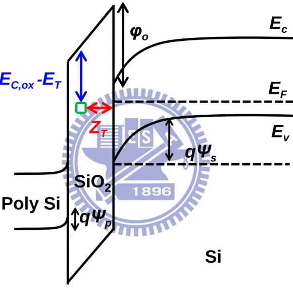
Figure 2.1 (a) shows the schematic diagram of RTN (random telegraph noise) noise with drain current fluctuation. The probability of a transition from the high current state to the low current state is given by 1/τe. Similarly, the probability of a transition from the low
current state to the high current state is 1/τc. ET in thesis is the energy of the trap, and the
EF is Fermi energy for electrons. Based on the principle of detailed balance, the average
emission time is given by [2.3]:
. (2.1) − = kT E E g T F e c exp _ _ τ τ
12
Here, k is the Boltzmann constant, T is the temperature, τc and τe are average capture time
and emission time, respectively, and g is the degeneracy factor. Therefore, let g = 1;
. (2.2)
where ECox is the conduction band edge of the oxide, EC is the conduction band edge of
silicon, φo is the difference between the electron affinities of Si and SiO2, VFB is the
flat-band voltage, φs is the amount of band-bending, ZT is the position of the trap in the
oxide measured with respect to Si-SiO2 interface, Tox is the oxide thickness, VGS is the
gate-source voltage, and q is electronic charge. The right-hand side of Eq. (2.2) represents the difference between trap energy level and electron’s Fermi level. We can easily recognize the energy difference from Fig. 2.2.
By differentiating (2.2) with respect to VGS, the position of the trap in the oxide ZT
can be obtained by the following equation:
. (2.3)
(
)
(
)
_ , 0 _ 1 ln c [ T ( )] C ox T C Fn s gs FB s p ox e Z E E E E q q V V kT T τ φ ψ ψ ψ τ = − − − − − + + − − − _ _ (ln ( /c e)) T ox gs d kT z T q dV τ τ = −13
2.2.2 Lateral Profiling Method
Because the RTN signals are more sensitive to the peak of the channel potential barrier, and the barrier peak is dependent on the source-to-drain voltage; the trap position in the channel direction can be defined. Fig. 2.3 shows the barrier peaks fluctuated by oxide traps. The emission/capture charge on the local trap causes barrier peaks raised/suppressed directly, and the drain current would suffer from the barrier scattering seriously. By increasing source-to-drain voltage, the barrier peak will be shifted from the middle of the channel to the drain side. The relation between source-to-drain voltage and the position of barrier peak cane be derived as below:
(2.4)
. (2.5) where Ypeak is the position of barrier peak at given VDS, Y0 is the barrier peak at VDS =
0.05V, Leff is the effective channel length, ΔL is depletion region length at given VDS;
which used to adjust the channel length, S.S.0 is the subthreshold Id swing at VDS = 0.05V,
S.S. is the subthreshold Id swing at given VDS, Vbi is junction barrier between source and
channel, Vc,max is barrier heigh of long channel, as shown in Fig. 2.4.
To extract the trap position, we extract Vbi , Vc,max , and ΔL experimentally.
(
)
(
)
60
.
.
60
.
.
0 0 , max , max , 0
mV
S
S
mV
S
S
C
C
L
L
L
V
V
DIBL
V
V
L
L
Y
Y
dm dm eff eff c bi c bi eff peak−
−
=
=
D
−
−
−
−
=
D
−
−
14
2.3 Device Preparation and Experimental Setup
2.3.1 Device preparation
The 28nm technology node of the bulk trigate CMOS devices with poly-Si gate made on a pilot foundry platform, with EOT(SiO2)= 20Å were prepared as shown in Figs.
2.5. Also bulk-planar devices on the same technology node were made for comparisons as shown in Figs. 2.6.
2.3.2 Experimental Setup
The experimental setup for the current-voltage measurement of devices is illustrated in Fig. 2.7 and Fig. 2.9, respectively. Each of the analyzers is connected by the co-axial or tri-axial cable including the semiconductor parameter analyzer (HP 4156C) as shown in Fig. 2.7. In order to suppress the noise of transport, we connect the parameter analyzers directly without switch mainframe, while the RTN signal is measured, as shown in Fig. 2.8. The Cascade guarded thermal probe station, and a thermal controller. This facility provides an adequate capability for measuring the low leakage devices MOSFET characteristic. Therefore, our group developed a control system in HT-Basic language. Through
15
IEEE-488 (GPIB) cable, we can directly give the order to each analyzer. From the above system, the I-V and C-V characteristics of the MOSFET devices can be precisely performed.
While measuring the RTN signal, we set the interval time and the total measure points in the beginning. Then, to calculate both the high level state time and the low level state time of Id, we can get the average τc and τe . In this experiment the gate voltage is biased at
16
τ
c
∆I
D
τ
e
I
D
Time
(a)
(b)
Fig. 2.1 (a) Illustration of the three parameter of the RTN noise: capture time τc, emission
time τe, and current amplitude ΔID. (b) Carrier trapping and detrapping by the
slow trap near the drain side.
Trap
Capture
Emission
17
E
c
E
v
E
F
φ
o
E
C,ox
-
E
T
Z
T
q
Ψ
s
q
Ψ
p
SiO
2
Si
Poly Si
Fig. 2.2 The energy band diagram of the Si-SiO2 interface in the channel at the trap
18
Fig. 2.3 Oxide trap RTN induce barrier peak fluctuate: Vth variation is dominated by the
19
Fig. 2.4 A new model is to approximate the carrier peak in the channel as a second degree
curve, in which the peak position can be determined by the DIBL.
Gate
S
D
y
ΔL + L”
eff=
L
effV
bi 0V
c,maxV
c(V
sd)
DIBL
Y
0Y
peak20
Y
Y
+
Y
Y
+
Poly
Gate
STI
STI
Oxide
Cha
nne
l
Fig. 2.5 (a) The 3D schematic of bulk trigate device used in this work. (b) The
21
S
D
Poly
Gate
Bulk planar devices
22
Fig. 2.7 The experimental system of current-voltage (I-V) for both n-type or p-type MOSFET.
23
Parameter Analyzer HP 4156C
PC
Probe Station
Fig. 2.8 The measurement setup using Analyzer HP 4156C to do the sampling of RTN signals.
24
Substrate
Source
Drain
V
GSV
DSGate
Poly
Oxide
25
Chapter 3
Influence of Multi-level RTN in Trigate MOSFET
And the Distribution of Oxide Trap Through 2-D
Profiling
3.1 Introduction
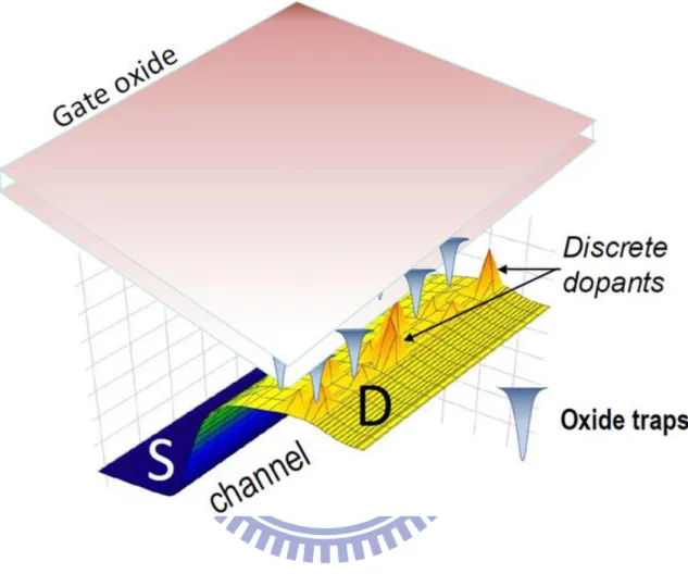
As Intel co-founder Gordon Moore’s bold prediction, popularly known as Moore's Law, states that the number of transistors on a chip will double approximately every two years. Electrical engineer which has maintained this pace for decades, this golden rule as both a guiding principle and a springboard for technological advancement, driving the expansion of functions on a chip at a lower cost per function and lower power per transistor by introducing and using new materials and transistor structures. As VLSI scales toward 22nm node, the leakage and variation are intolerant in the planar devices. Therefore, finFET structure had been proposed since 1999 and been mass produced recently. However, there are several problems not solved in FINFET device, and RTN is one of the most important variation sources.
In this chapter we dedicated to profile the distribution of RTN traps to explain the influence of trap positions. In order to understand the difference between the planar
26
devices and the trigate devices, we used two kinds of devices in this experiment separately. On the other hand, we took the devices under stressed condition and fresh condition while measurement, to understand the difference between processing induced RTN and stress induced RTN. Since finFET devices just began to be used on mass product recently, the device quality was not very stable. Devices with defect might induce circuit failed and power consumption. Through this study, we can realize the drawbacks of produce process and improve the procedure.
3.2 Experimental
3.2.1 Process Induce RTN Trap
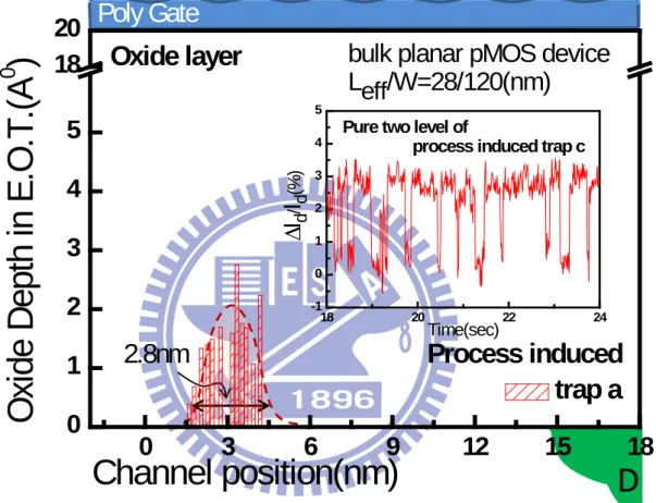
Figure 3.1 shows the result of a RTN trap in the planar pMOS device. According to our experiment, the trap distribution is a Gaussian-like shape. To understand the reason of Gaussian-like distribution, we examine Eq. 3.1 and Eq. 3.2 below.
− = kT E E g T F e c exp _ _ τ τ , (3.1)
V
K
T
Z
g e c B OX T d d q T (ln( ))τ
τ
− = . (3.2)27
the trap energy, ET. However, the trap energy is a distribution rather than a constant. The
trap distribution is dependent on the channel position.
The difference between oxide trap energy level and Fermi level is changed by gate voltage and determines the ratio of capture time and emission time. Through physical methodology, we can find the relationship between time constants and trap energy and Fermi level with trap depth.
Fig. 3.2 is the result of RTN traps in the planar nMOS devices. The figure demonstrates that there are two traps in the planar nMOS device. From the profiling result, the different depths of two traps can be observed easily in this profiling method. We also observed that the two traps interact in the middle of them. To discuss the profiling result, we can examine the ΔID /ID curve as shown in Fig. 3.3. Depending on the trap location, 3
cases of RTN signal can be observed in the ΔID /ID curve, from which the case 1 and the
case 3 are two-level signals, but the case 2 is four-levels in the interaction region because the barrier peak is affected by the two overlapping traps.
Figure 3.4 shows the profile of single RTN trap in a trigate pMOS device, and Fig. 3.5 shows the profile of a bulk-trigate nMOS device. By comparing the trap profiling results of bulk-trigate devices with the planar devices, the broader distributions can be observed in both nMOS devices and pMOS trigate devices. From the result, we make an assumption that the deeper RTN trap might induce boarder distribution. Fig. 3.4 shows the single trap
28
profile, and Fig. 3.5 shows the profile of two RTN traps without overlapping. Comparing Fig. 3.2 and Fig. 3.5, we realize that if the two traps separate far enough, the signals are always two-levels. Because both traps are not overlapped, no 4-level RTN is observed. On the other hand, if the two traps are so close that the trap energy overlapped thus it will induce four-level RTN signals in the overlapped region.
By differentiating equation 3.1 with VGS, the position of the trap in the oxide is
conventionally obtained. Fig. 3.6 shows positive dependency of ln(τc/τe) on VGS for planar
devices and negative dependency for trigate devices. The RTN-traps in the trigate devices tend to exchange with gate, but the RTN-traps in the planar devices tend to exchange with channel. Because the trap depths in the trigate devices are deeper than that in the planar devices as shown in Fig. 3.7. As a result, Fig.13 outlines the information of process induced RTN traps.
We also got the cross-sections of RTN traps by examining the profiling result. Fig. 3.9 compares the cross-sections of RTN traps with reported data [3.1], [3.2], and theory value, showing good consistency.
29
3.2.2 Stress Induce RTN Trap
Since SRAM is highly vulnerable to mismatch, and the devices might be stressed while operating; to understand the stressed devices impact on circuits is important. To understand the behavior of post-stressed SRAM, we utilize different stress mechanisms, hot carrier (HC) stress and NBTI stress for the nMOS devices and the pMOS devices respectively. HC means carriers gain enough energy to enter the conduction band. We used drain avalanche to get the hot carrier. This occurs when a high drain voltage is applied under non-saturated conditions, and results in the very high electric fields near the drain, which accelerates channel carriers into the drain's depletion region. Studies have shown that the worst effects occur when VD = 2VG. Instead of HC stress, we utilize NBTI stress for pMOS devices. In
the sub-micrometer devices nitrogen is incorporated into the silicon gate oxide to reduce the gate leakage current density and prevent the boron penetration. However, incorporating nitrogen enhances NBTI. It is possible that the interfacial layer composed of nitride silicon dioxide is responsible for those instabilities. This interfacial layer results from the spontaneous oxidation of the silicon substrate. To limit this oxidation, the silicon interface is saturated with nitrogen resulting in a very thin and nitride oxide layer. In the case of NBTI, it is believed that the electric field is able to break Si-H bonds located at the Silicon-oxide interface. H is released in the substrate where it migrates. The remaining
30
dangling-bond contributes to the threshold voltage degradation.
Figure 3.10 shows the result of HC-induced two traps in the planar nMOS devices. As people know, the carrier energy is usually raised on the high field region. The depletion region is the region of the highest electric field. Therefore, HC-induced traps tend to cluster in near drain region closely. From our research before, we got a conclusion that different RTN traps might interact with each other, if the energy band overlaps. Therefore, the profile of RTN traps after HC stressed is three regions separately, including the left-trap region, the right-trap region, and the overlapped region. Because these two RTN signals are quite different, it is beneficial to analyze. Otherwise, the RTN signal would become mess and hard to be analyzed. Fig. 3.11 shows the ID RTN signals of these separate regions. In
the overlap region, the ID RTN signal is raised to a 4-level RTN obviously.
Figure 3.12 shows the result of NBTI-induced RTN traps in the planar pMOS devices. The RTN traps tend to be generated in the middle of channel, because NBTI-stress bias on VG=-2V only, and without VD bias.
After the experiment upon, the stress condition the trigate devices we used on is similar to that we used on the planar devices. Fig. 3.13 shows HC stress in trigate nMOS devices. The similar trap distribution can be observed on Fig. 3.11 and Fig. 3.13. Although the bulk-trigate structure and the bulk-planar structure are different, HC-induced RTN traps are usually generated in the vicinity of drain region. It is because the contribution of the
31
highest field is there. Likewise, we use NBTI stress in the trigate pMOS devices. Fig. 3.14 shows the profiling result of NBTI-induced RTN traps, and the two fully-overlapped traps are observed. It is because these two traps located in the same position in channel direction, but the vertical positions are different. Besides, we find that these two traps exclude each other to induce three-level RTN. Fig. 3.15 (a) shows the schematic, these two traps are barely aligned together. When one trap is occupied, it will repulse the other to capture the carrier as shown in Fig. 3.15 (a) & (b).
32
Poly Gate
D
2.8nm
0
3
6
9
12
15
18
0
1
2
3
4
5
18
20
trap a
Process induced
Oxide layer
bulk planar pMOS device
L
eff
/W=28/120(nm)
Channel position(nm)
O
xi
de D
ept
h i
n E
.O
.T
.(
A
0
)
18 20 22 24 -1 0 1 2 3 4 5DI
d /I
d (%) Time(sec)Pure two level of
process induced trap c
Fig. 3.1 The profiling result of the process-induced single RTN in the bulk planar pMOS devices, showing a Gaussian-like profile. The insert is the ΔId/Id
33
0
3
6
9
12
15
18
0
2
4
6
8
18
20
Process induced
O
xi
de
D
ept
h
in
E
.O
.T
.(
A
0
)
Channel Position(nm)
trap b
trap c
bulk planar nMOS device
L
eff
/W=29/120(nm)
Oxide layer
D
Poly Gate
Case1( only trap a)
Case2( trap a+ trap b)
Case3( only trap b)
2.3nm
3.1nm
Fig. 3.2 The profiling result of process-induced multi-RTN in the bulk planar nMOS devices, showing 2 Gaussian-like packets, traps b & c. Note that we categorize this result into the Case 1, 2, and 3. For the Case 2, two packets are overlapped in tails.
34
18
19
20
21
22
-1
0
1
2
3
5
10
15
20
25
30
-4
-2
0
2
4
18
19
20
21
22
-2
0
2
4
6
Case3- trap c induced 2 level RTN
Case2- trap b & c induced 4 level RTN
Case1- trap b induced b level RTN
Lv.4
Lv.3
Lv.2
DI
d
/
I
d
(%)
Lv.1
Time(sec)
Fig. 3.3 The result of the profiling of the process-induced two-RTN traps in the bulk trigate nMOS devices, showing 2 Gaussian-like waveforms, but both waveforms are not overlapped because of a large distance between them.
35
D
0
3
6
9
12
15
18
0
4
8
12
16
20
Process induced
trap d
O
xi
de D
ept
h i
n E
.O
.T
.(
A
0
)
bulk trigate pMOS device
L
eff
/W=28/100(nm)
Oxide layer
Channel position(nm)
Poly Gate
7.6nm
Trap depth
Trap cross-section
Fig. 3.4 The result of the profiling of the process-induced single-RTN in the bulk trigate pMOS devices, showing a Gaussian-like distribution.
36
D
0
3
6
9
12
15
18
0
4
8
12
16
20
Channel position(nm)
O
xi
de D
ept
h i
n E
.O
.T
.(
A
0
)
Process induced
bulk trigate nMOS device
Leff/W=29/100(nm)
Oxide layer
trap e
trap f
Poly Gate
3.6nm
No overlapped and
interacted b/w two
RTN traps
3.75nm
Fig. 3.5 The result of the profiling of the process-induced two-RTN traps in the bulk trigate nMOS devices, showing 2 Gaussian-like waveforms, but both waveforms are not overlapped because of a large distance between them.
37 -0.06 -0.03 0.00 0.03
0.0
0.2
0.4
0.6
-0.06 -0.03 0.00 0.03-2
-1
0
1
2
ln
(τ
c
/τ
e
)
V
gs
-V
t
(volt)
ln
(τ
c
/τ
e
)
bulk planar pMOS devices Leff/W=28/120(nm)
Vds=0.05V Vds=0.3V
Vds=0.6V Vds=0.9V Vds=1.2V bulk trigate pMOS devices Leff/W=28/100(nm)
begative
dependent
Positive
dependent
trap B gs e cT
T
k
q
V
=
∂
∂
ln(
τ
τ
)
Fig. 3.6 (left) the ln(τc/τε) dependency of the bulk planar pMOS devices, showing
the positive dependency, but (right) the bulk trigate devices shows the negative dependency.
38
Fig. 3.7 From judging the RTN proofing data and ln(τc/τe) dependency, we conclude
that (up) RTN of planar devices are near the interface between the oxide and Si; (down) RTN of trigate devices are near the interface between the oxide and poly-Si.
SiO
2
Carrier
Trap
PolySi
Si sub.
SiO
2
Carrier
Trap
PolySi
Si sub.
39 Oxide depth in E.O.T(A0) Electron potential (ev) 3 2.25 1.5 0.75 10 5 0 15 20
: RTN trap site of bulk
planar CMOS devices
:RTN trap site of bulk
trigate CMOS devices
PolySi SiO2 Si p sub.
10 5 0 15 20 Oxide depth in E.O.T(A0) Electron potential (ev) 4 2 3 1 Si n sub.
40
0
1
2
3
4
R
adi
us
of
c
ros
s-sec
tion
of
R
T
N
t
rap(
nm
)
trap a b c d e
f
ref.8 ref.9Calculated screening length
this work
Fig. 3.9 The comparisons of the cross-section of the process-induced RTNs in this work. The reported data and the theoretical value show good consistency.
41
D
0
3
6
9
12
15
18
0
4
8
12
16
20
O
xi
de D
ept
h i
n E
.O
.T
.(
A
0)
V
ds=V
gs=2V,10s
HC stress@
bulk planar nMOS device
Leff/W=29/120(nm)
Oxide layer
trap g trap hChannel position(nm)
Stress induced
Poly Gate
Case1( only trap g)
Case2( trap g+ trap h) Case3
(only trap h)
2.8nm
3nm
Fig. 3.10 The result of the HC stresss-induced multi-RTN in bulk planar nMOS devices, showing 2 Gaussian-like packets, traps g & h with strong interference. We categorize this result into the Case 1, 2, and 3. For the Case 2, two packets are overlapped in tails.
42
0
100
200
300
400
500
600
-3.0
-1.5
0.0
150
180
210
240
270
300
-4
-2
0
2
160
170
180
190
200
-1.5
0.0
1.5
3.0
Case3- trap h induced 2 level RTN
Case2- trap g & h induced 4 level RTN Case1- trap g induced 2 level RTN
Lv.4 Lv.3 Lv.2
DI
d
/
I
d
(%)
Lv.1Time(sec)
trap h trap gFig. 3.11 Cases 1, 2, & 3 addressed in Fig. 3.10. Case 1 shows clear 2 level of ΔId/Id for
trap-g induced RTN, and the Case 3 is the same for trap-h. But the Case 2 shows 4-level behavior composed by the trap-g & trap-h. Lvs.1 &2 are contributed from the trap-h, the others are from the trap-g.
43
D
-3
0
3
6
9
12
15
18
0
5
10
15
20
O
x
ide D
ept
h i
n E
.O
.T
.(
A
0)
trap i
Stress induced
NBTI stress@
V
GS
=-2V, 100
0C, 10sec
bulk planar pMOS device
L
eff
/W=28/120(nm)
Oxide layer
Channel position(nm)
Poly Gate
6nm
Oxide
Poly Gate
D
CarrierNBTI-induced-RTN-trap near channel
middle
Trap
Fig. 3.12 The result of the NBTI stress-induced single-RTN in the bulk planar pMOS devices, showing a Gaussian-like shape. Note that this shape distributes near the middle of the channel region.
44
D
0
3
6
9
12
15
18
0
4
8
12
16
20
Channel position(nm)
V
ds=V
gs=2V,10s
HC stress@
bulk trigate nMOS device
L
eff
/W=29/100(nm)
Oxide layer
O
xi
de D
ept
h i
n E
.O
.T
.(
A
0
)
stress induced
trap j
Poly Gate
4.5nm
Oxide Poly GateD
CarrierHC-induced-RTN-trap near drain side
Trap
Fig. 3.13 The result of the HC stress-induced single-RTN trap in bulk trigate nMOS devices, showing a bell shape. Note that this shape distributes near the region of drain side.
45
D
Poly Gate
NBTI stress@
V
GS=-2V, 100
0C, 10sec
trap kstress induced
0
3
6
9
12
15
18
0
5
10
15
20
O
xi
de D
ept
h i
n E
.O
.T
.(
A
0
)
bulk trigate pMOS device
Leff/W=28/100(nm)
Oxide layer
trap l
Channel position(nm)
Two b.TI induced
RTb traps totally
overlapped
Case 1
Fig. 3.14 The result of the NBTI stress-induced 2-RTN traps in bulk trigate nMOS devices. These two traps are totally overlapped in the shape and aligned on the same channel position with very close trap depths.
46
trap-k trap-l
: de-trapped state : trapped stateLv.1
Lv.2
Lv.3
no Lv.4
SiO
2 CarrierPolySi
Trap l trapped carrier. Trap k cannot trap another carrier.
Due to Coulomb repulsive force of the
trapped trap, there is no Lv.4.
Carrier
Trap k trapped carrier. Trap l cannot trap. another carrier either
Fig. 3.15 (a) The 3 level RTN was observed in the Case 1 addressed in Fig. 3.14. There is no Lv.4, which two traps are overlapped. This is due to the fact that Coulomb repulsive force of a trapped trap rejects the trapping process of empty trap, (b) & (c).
47
Chapter 4
The Applications of Multi-RTN: The Impact on SRAM
Operation & The Manipulation of RTN-trap Positions
4.1 Introduction
In this chapter, we will be focused on the influence of device variation on circuits, especially for SRAM. As microprocessors and other electronic applications get faster and faster, the need for large quantities of data at very high speeds increases, while providing the data at such high speeds get more difficult to accomplish. Besides, the manipulation of RTN-trap positions has been demonstrated by utilizing different stress methods. It will reveal a new scenario of the discrete-bit storage on SONOS or nano-crystal memory cells in the future.
As microprocessor speed increases from 25 MHz to 1GHz and beyond, system designers have become more creative in their use of cache memory, interleaving, burst mode, and other high-speed methods for accessing memory. The old system sporting just an on-chip instruction cache, a moderate amount of DRAM and a hard drive have given way to sophisticated designs using multi-level memory architectures. One of the primary building blocks of the multi-level memory architecture is the data cache.
48
According to our previous research, RTN traps induced by excessive mechanical stress are correlated to leakage current in very high-density SRAM devices, especially multi-RTN, and it will degrade the RSNM severely.
Finally, we are interested in the manipulation of RTN-trap positions. In the previous study, we found that the RTN-trap position is dependent on the stress methods, and therefore, we may control the trap positions by the HC stress or the FN stress.
Hot-carrier emission is expected to be accelerated in the depletion region. Electrons gain energy through channel potential. While electrons get 3.2eV, it will be injected from the conducting band in the silicon substrate to the gate dielectric, and it is probable to break either a covalent or a Si-H bond randomly. Because the HC-stress will induce electron-hole pairs, by monitoring the substrate current, we can distinguish the extent of hot carriers. A high substrate current means a large number of created electron-hole pairs and therefore an efficient Si-H bond breakage mechanism. When interface states are created by HC stress, the threshold voltage is modified, and the subthreshold slope is degraded.
According to the principle of HC stress, it can be used to control the RTN traps generated at the drain edge. Moreover, the maximum electric field will be shifted toward the center of the channel by modifying the drain voltage, and the traps will be generated there. Through the profiling result, we found that the traps are generated at the region
49
between the channel middle and the drain edge actually. In the final part, we utilize the FN stress to generate RTN-traps in the center of channel. In the previous measurement result, we found that the RTN traps are located in the center of the channel through NBTI stress. Hence, we consider that the electric field distribution of NBTI stress is similar to that of FN stress in nMOS devices. After the measurement, the manipulation of RTN-traps in the channel which is generated by different stress conditions has been observed.
4.2 The Basics of SRAM
4.2.1 SRAM Operations
The SRAM cell consists of a bi-stable flip-flop connected to the internal circuitry by two access transistors as shown in Fig. 4.1. When the cell is not addressed, the two access transistors are closed, and the data is kept to a stable state, latched within the flip-flop.The flip-flop needs the power supply to keep the information. The data in an SRAM cell is volatile. However, the data does not “leak away” like in a DRAM, so the SRAM does not require a refresh cycle.
Figure 4.2 shows the read/write operations of an SRAM. To select a cell, the two access transistors must be “on” so the elementary cell (the flip-flop) can be connected to
50
the internal SRAM circuitry. These two access transistors of a cell are connected to the word line (also called row or X address). The selected row will be set at VCC. The two
flip-flop sides are therefore connected to a pair of lines, B and . The bit lines are (also called columns or Y addresses). During a read operation, these two bit lines are connected to the sense amplifier that recognizes if a logic data “1” or “0” is stored in the selected elementary cell. This sense amplifier then transfers the logic state to the output buffer which is connected to the output pad. There are as many sense amplifiers as the output pads. During a write operation, data come from the input pad. It then moves to the write circuitry. Since the write circuitry drivers are stronger than the cell flip-flop transistors, the data will be forced onto the cell. When the read/write operation is completed, the word line (row) is set to 0V, the cell (flip-flop) either keeps its original data for a read cycle or stores the new data which was loaded during the write cycle.
4.2.2 Steady Noise Margin
The SRAM cell immunity to static noise is measured in terms of SNM that quantifies the maximum amount of voltage noise that can be tolerated at the cross-inverters output nodes without flipping the cell. The graphical method to determine the SNM uses the static voltage transfer characteristics of the SRAM cell inverters.
51
4.2.3 Impact of Multi-level RTN on SRAM
Figure 4.3 is a 6T SRAM and TEM picture. To study RTN impact on SRAM carefully, we defined two cases of multi-RTN traps generated in different transistors. The two cases including RTN traps are generated on the pull up transistor only, and RTN traps generated on both pull-up transistor and pull-down transistor, as shown in Fig. 4.4. Because the RTN signals induce the Vt disturbance, the Vt of device with RTN will become multi-level.
Figure 4.5 shows the butterfly curve of planar SRAM under the case 1, pull-up transistor with multi-RTN signals. It has been observed that the butterfly curves split into 4-levels (the insert). Fig. 4.6 shows the RTN signals measured in pull-up transistor, and 4-levels can be pointed out demonstratively. It is the reason for the butterfly curves split into 4-levels. The similar phenomena can be observed in the trigate SRAM. Fig. 4.7 shows the butterfly curves of the trigate SRAM also split into clear 4-level transition under the same case. Fig. 4.8 shows the ID RTN signals measured in the pull-up transistor, and
4-levels can be demonstrated. Comparing the butterfly curves of the planar SRAM with the trigate SRAM, the butterfly curves of trigate SRAM separate widely. It is because the RTN amplitude of the trigate devices is larger than that of the planar devices. Fig. 4.9 shows the comparison of σRSNM between the planar devices and the trigate devices under the case 1. From the figure, we realize that the σRSNM increases severely, due to the RTN generation
52
under the case 1. Besides, the σRSNM for trigate SRAM is much larger than the planar SRAM under this case. From the result of our research, we also found that σRSNM depends on the amplitude of RTN signals.
Figure 4.10 shows the butterfly curves of the planar SRAM under the case 2, M2 and M3 with multi-RTN. It has been observed that the butterfly curves translate fail because of RTN signals. Note that the insert shows a noticeable component of transition failure. Fig. 4.11 shows the results of multi-RTN induced trigate SRAM failure on transition, which is due to a wide Vt-shift of M3 raised by the trapping and de-trapping of multi-RTN traps.
When Vt is shifted by RTN process upon the trigger voltage of SRAM, the transition will
be immediately failed, Fig. 4.12 The larger multi-RTN induced Vt shift is, the higher the
probability of transition failure raises.
4.3 The Manipulation of RTN-trap Positions
Figure 4.13 shows the schematic of hot-carrier stress under VG= VD= 2V bias
condition and indicates that the impact ionization region is close to the drain edge while the drain voltage is increased. Fig. 4.14 shows the measurement result of the hot carrier stress under this condition, and the traps profile is approached to the drain side actually.