國立交通大學
電子工程學系 電子研究所碩士班
碩 士 論 文
非揮發性記憶體的儲存電荷的空間分佈對
元件特性的影響
Effects of Spatial Distribution of the Stored-Charge
on Device Characteristics of Non-volatile Memory
研 究 生:余昆武
指導教授:崔秉鉞 教授
非揮發性記憶體的儲存電荷的空間分佈對
元件特性的影響
Effects of Spatial Distribution of the Stored-Charge on
Device Characteristics of Non-volatile Memory
研究生:余昆武 Student : Kun-Wu YU
指導教授:崔秉鉞 Advisor : Bing-Yue Tsui
國立交通大學
電子工程學系 電子研究所
碩士論文
A thesis
Submitted to Department of Electronics Engineering & Institute of Electronics
College of Electrical and Computer Engineering
National Chiao Tung University
in Partial Fulfillment of the Requirement
for the Degree of Master
in
Electronic Engineering
2009
Hsinchu, Taiwan, Republic of China
非揮發性記憶體的儲存電荷的空間分佈對
元件特性的影響
研究生: 余昆武 指導教授: 崔秉鉞
國立交通大學電子工程系 電子研究所碩士班
摘 要
在本論文中,探討了非揮發性記憶體的儲存電荷的空間分佈對元件特性的影 響。根據模擬的結果,調變臨界電壓(Vt)和調變閘極引發汲極漏電流(GIDL)是與 電荷儲存的位置有關。當電荷儲存在通道中央的上方位置時,整個次臨界曲線會 向右移,這是由於負電荷在捕陷電荷層的正中央會造成通道區域的電子位障上 升。當電荷儲存在通道的上方並且靠近汲極的接面時,只有上半部份的次臨界曲 線會向右移。這是因為通道區域中的電子位障被汲極電壓稍微地拉低了,所以下 半部份的次臨界曲線不會移動,但是電子位障仍然不夠低,不足以讓電子完全地 導通,所以上半部份的次臨界曲線會向右移。再來,當電荷儲存的位置正好在汲 極接面的正上方時,閘極引發汲極漏電流會大量地增加。這是因為在閘極和汲極 間的垂直電場變強了,所以閘極引發汲極漏電流會上升。長通道元件和短通道元 件有相似的儲存電荷的空間分佈對元件特性的影響。 此外,我們證實在 N 型通道的多晶矽/氧化鋁/氧化鉿/氧化矽/矽(SAHOS)記 憶體元件上單一位元胞中可以有三位元的記憶體特性。為了增加水平方向上的電 荷儲存空間,我們把捕陷電荷層延伸到側壁空間層的底下。結合調變臨界電壓、調變正向讀取的閘極引發汲極漏電流以及調變反向讀取的閘極引發汲極漏電 流,這些記憶體元件可以有三位元的操作。這些元件中,源極/汲極與閘極重疊 的結構顯示出比非重疊的結構有較好的記憶體性能。在源極/汲極與閘極重疊的 元件上,臨界電壓可以位移產生 7V 的記憶窗口,並且在外插到十年線後仍擁有 良好的儲存資料持久性。此外,在 105次寫入/抹除之後,此記憶體元件在調變 臨界電壓上仍維持良好的性能。當此記憶體元件被運用在NOR 型的非揮發性記 憶體的陣列結構中,干擾效應對於臨界電壓來說是可以忽略的。閘極引發汲極漏 電流可以在調變後產生約100 倍大小的差異,但是沒有良好的儲存資料持久性, 也沒有良好的耐操度。因為電荷是儲存在靠近側壁空間的角落,所以「水平電荷 遷移」和增加電荷流失速率的缺陷都是造成沒有良好的儲存資料持久性的原因。 而沒有良好的耐操度的可能原因是在每一次的寫入/抹除之後,儲存電荷的空間 分佈改變了。對元件的可靠度來說,汲極的干擾效應對於閘極引發汲極漏電流是 個問題。
Effects of Spatial Distribution of the Stored-Charge
on Device Characteristics of Non-volatile Memory
Student: Kun-Wu Yu Advisor: Bing-Yue Tsui
Department of Electronics Engineering
Institute of Electronics
National Chiao Tung University
Abstract
In this thesis, the effects of spatial distribution of the stored-charge on device characteristics of non-volatile memory are evaluated. According to the simulated results, the modulation of the threshold voltage (Vt) and the modulation of the
Gate-Induced-Drain-Leakage (GIDL) are related to the stored-charge positions. When the charges are stored at the position which is above the channel center, the whole subthresthold curve is moved to the right because of the negative charges stored at the center of the trapping layer resulting in a raise of the electron barrier of the channel region. When the charges are stored at the position which is above the channel and near the drain junction, only the upper half subthresthold curve is moved to the right. Because the electron barrier of the channel region is slightly dragged down by the drain voltage, the lower half subthreshold curve keeps. However, the electron barrier is not low enough to allow complete electron conduction, so the upper half subthresthold curve is moved to the right. Next, when the charges are stored just
above the drain junction, the GIDL current increase largely. Because the vertical electric field between the gate and the drain is enhanced and then results in larger GIDL current. Both the long channel device and the short channel device have the similar effects of stored-charge distribution on device characteristics.
Moreover, the 3-bit per cell memory characteristics are demonstrated on the n-channel poly-Si/Al2O3/HfO2/SiO2/Si (SAHOS) memory device. In order to increase
lateral charge storage space, the HfO2 charge trapping layer extends to the underneath
of the spacer. The 3-bit operations of these memory devices are demonstrated by combining the Vt modulation, the GIDL current modulation on forward read, and the
GIDL current modulation on reverse read. The devices with the S/D-to-gate overlap structure show better memory performances than those with S/D-to-gate non-overlap structure. For the devices with the S/D-to-gate overlap structure, the Vt can shift with
large memory window of 7V, and shows good 10-year extrapolated charge retention. Moreover, high endurance after 105 P/E cycles is exhibited on the Vt modulation. The
disturbance effects of the Vt are negligible when this memory device is implemented
by the NOR array architecture. The GIDL current can be modulated by about two orders of magnitude, but it shows poor retention and poor endurance. Because the stored charges are near the corner of the spacer, poor retention is due to “lateral charge migration” and the defects which enhance charge loss rate. The poor endurance is possible as a result of the change of the stored charges distribution after every P/E cycle. In addition, the drain disturbance on the GIDL is also an issue for device reliability.
誌 謝
隨著論文的完成,碩士生涯也到了尾聲。在寫論文的這一年多裡,我受到許 許許多多的人幫助,使我能夠順利地完成我的碩士論文,謹以此文表達我的感謝。 首先,我要感謝我的指導教授 崔秉鉞老師。不管是做研究的態度還是做研 究的方法,老師都給我很大的助益。老師在研究上非常正直,對於是非對錯總是 秉持著自己的原則,不會得過且過,這樣的態度給了我很多正面的思考。另外, 老師在訓練學生培養研究能力上,更是仔細謹慎,不管是做實驗的技巧或是實驗 現象背後的學理,老師都會抽絲剝繭地與學生們討論,並且傾囊相授。然後,我 還要特別感謝老師非常有耐心地逐字逐句修改我的論文,給予我許許多多的建 議,老師您辛苦了! 其次,我要感謝財團法人工業技術研究院提供沉積氧化鋁和氧化鉿的服務, 感謝工研院蔡銘進組長和辜佩儀工程師在元件的製作上給予許多協助。另外,我 也要感謝國家奈米元件實驗室與國立交通大學奈米中心提供半導體製程的機台 設備,還有許多機台工程師與小姐們的幫忙。 感謝實驗室的謝志民、盧季霈、羅正愷學長給予許多研究上的建議,感謝李 振銘學長教我實驗機台並且給予很多實驗上的協助。謝謝同學瑞堯、俊凱、依成 在實驗與修課上的協助與砥礪,也謝謝學弟們這一年的陪伴。另外還要特別感謝 另一個實驗室的陳建華學長,每次教我機台都非常地仔細。還要感謝凱瑜常常在 我研究的低潮時勉勵我。 最後,我要感謝我的家人們!謝謝爸爸媽媽一直以來的栽培與付出,對於我 求學的路上總是給予許許多多的支持與勉勵,對於我的生活起居更是照顧的無微 不至。還有我親愛的弟弟,一直扮演我的家人、朋友與玩伴三種角色,在我人生 的路上帶給我很多的快樂。另外,還有很多一直為我打氣的親朋好友們,謝謝你 們!Contents
Abstract (Chinese)………...….I
Abstract (English)………...III
Acknowledgement (Chinese)………..…V
Contents………..VI
Table Captions………IX
Figure Captions………...X
Chapter 1 Introduction….………1
1-1 Evolution of Non-volatile Memory……….………..……….1
1-1-1 Floating Gate Non-volatile Memory…..………...…2
1-1-2 SONOS Non-volatile Memory………..3
1-1-3 Nano-crystal Non-volatile Memory………..5
1-1-4 Non-charge-based Non-volatile Memory………..6
1-2 Motivation………7
1-3 Thesis Organization………9
Chapter 2 Experimental Procedure………...14
2-1 Simulation Method….………...14
2-1-1 Device Structure……….……….14
2-1-2 Physical Models………...15
2-2 Device Fabrication………16
2-3 Electrical Characterization Techniques……….…18
2-3-1 P/E speed and memory window………..19
2-3-3 Endurance………20
2-3-4 Disturbance………..21
Chapter 3 Simulation Results of Stored Charge Distribution on
Device Characteristics……….29
3-1 Introduction…….………..29
3-2 Long Channel SONOS type NVM………..30
3-2-1 Overlap between S/D and gate.………...30
3-2-2 Non-overlap between S/D and gate……….31
3-3 Short Channel SONOS type NVM………..32
Chapter 4 Characteristics of SAHOS Non-volatile Memory……...45
4-1 Introduction………...45
4-2 Device Structure Inspection……….45
4-3 Multi-bit Operation………..46
4-3-1 Sample B and C: Sufficient gate to source/drain overlap……....47
4-3-2 Sample A: Insufficient gate to source/drain overlap………...49
4-4 P/E Speed and Memory Window……….50
4-4-1 Sample B: Sufficient gate to source/drain overlap………..50
4-4-2 Sample A: Insufficient gate to source/drain overlap………52
4-5 Retention Performance……….53
4-5-1 Sample B: Sufficient gate to source/drain overlap…………..…53
4-5-2 Sample A: Insufficient gate to source/drain overlap………55
4-6 Endurance Performance………..56
4-6-1 Vt modulation………..56
4-7 Disturbance Performance……….58
4-7-1 Read Disturbance……….60
4-7-2 Gate Disturbance……….61
4-7-3 Drain Disturbance………61
4-8 Summary………62
Chapter 5 Conclusions and Future Works………93
5-1 Conclusions…….………...93
5-2 Future Works……….95
References………97
Table Captions
Chapter 2
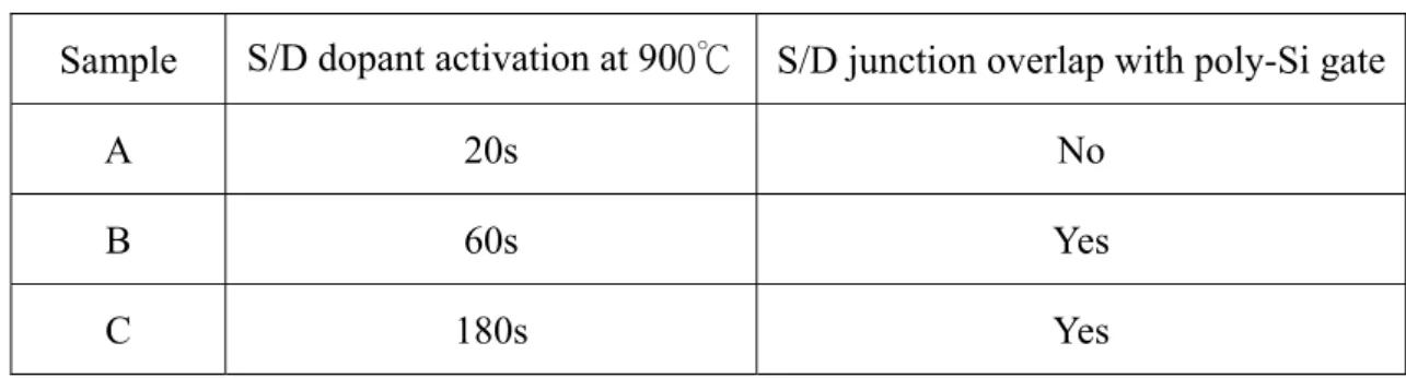
Table 2-1: Process conditions of the SAHOS non-volatile memory device fabricated in this thesis………22
Chapter 3
Table 3-1: The summary of the effects of stored-charge distribution on device characteristics for channel length 0.3 μm……….34 Table 3-2: The summary of the effects of stored charge distribution on device
characteristics for channel length 50 nm………..34
Chapter 4
Table 4-1: The 8 states of the Id-Vg and Is-Vg characteristics on sample B………….63
Figure Captions
Chapter 1
Fig. 1-1: Basic concept of floating gate (FG) non-volatile memory………11 Fig. 1-2: Basic concept of SONOS non-volatile memory………11 Fig. 1-3: Basic concept of nano-crystal non-volatile memory……….12 Fig. 1-4: (a) 2D schematic cross-section of the dual-bit FinFET SONOS NVM cell. (b)
Simulated IDS-VGS characteristics show that VT and GIDL can be used to
distinguish the state of Bit 1 and Bit 2. In this figure, ‘0’ (‘1’) refers to the programmed (erased) state [38]………12 Fig. 1-5: Schematic energy band diagrams of Al/Al2O3/HfO2/SiO2/p-Si (solid line)
and Al/SiO2/HfO2/SiO2/p-Si (dash line) memory structures under (a)
program and (b) erase modes [47]………13
Chapter 2
Fig. 2-1: Long channel device (a) device structure (b) structural parameters………..23 Fig. 2-2: Short channel device (a) device structure (b) structural parameters………..24 Fig. 2-3: Process flow and cross-sections of the poly-Si/Al2O3/HfO2/SiO2/Si
(SAHOS) non-volatile memory. (a) after LOCOS process, (b) after dielectric stack deposition and gate patterning, (c) after spacer formation, (d) after S/D ion implantation, (e) after S/D activation, (f) after gate hard mask removal and silicide formation, (g) after back electrode formation……….28
Chapter 3
Fig. 3-1: (a) Physical mechanisms of the GIDL (b) current-voltage characteristics of the GIDL phenomenon [50]……….35 Fig. 3-2: The Id-Vg characteristics with the stored-charges at various positions for the
long channel 0.3 μm device. (a) Position 1 “above channel center”, (b) Position 2 “above channel and 30nm away from drain junction”, (c) Position 3 “above channel and next to drain junction”, (d) Position 4 “above drain and next to drain junction”, (e) Position 5 “above drain and 30nm away from drain junction”………38 Fig. 3-3: Conduction band energy along the X-axis of the channel (a) without charge (b) stored-charge at Position 1………..39 Fig. 3-4: Conduction band energy along the X-axis of the channel with the
stored-charges at Position 2 as Vd = 1V and Vs = 0V…….………...40
Fig. 3-5: The Id-Vg characteristics with the stored-charges at various positions for the
long channel 0.4 μm device. (a) Position 1 “above channel center”, (b) Position 2 “above channel and 30nm away from drain junction”, (c) Position 3 “above channel and next to drain junction”, (d) Position 4 “above drain and next to drain junction”………..42 Fig. 3-6: The Id-Vg characteristics with the stored-charges at various positions for the
short channel 50 nm device. (a) Position 1 “above channel center”, (b) Position 2 “above channel and 3nm away from drain junction”, (c) Position 3 “above channel and next to drain junction”, (d) Position 4 “above drain and next to drain junction”………...44
Chapter 4
Fig. 4-1: The TEM image of the cross-section view on sample C………...64 Fig. 4-2: The high resolution TEM image of the gate stack dielectric on sample C....64 Fig. 4-3: The high resolution TEM image of the spacer region on sample C………..65 Fig. 4-4: Id-Vg and Is-Vg curves on sample B during the operations.
1st state: (Vg = -16V, Vd = 0V, Vs = 0V, for 0.1sec)
2nd state: 1st state + (Vg = 0V, Vd = +11V, Vs = 0V, for 0.1sec)
3rd state: 2nd state + (Vg = 0V, Vd = 0V, Vs = +11V, for 0.1sec)
4th state: 3rd state + (Vg = -16V, Vd = 0V, Vs = 0V, for 0.1sec)
+ (Vg = 0V, Vd = 0V, Vs = +11V, for 0.1sec)
5th state: 4th state + (Vg = 0V, Vd = +11V, Vs = 0V, for 0.1sec)
+ (Vg = +16V, Vd = 0V, Vs = 0V, for 0.1sec)
6th state: 5th state + (Vg = 0V, Vd = 0V, Vs = +11V, for 0.1sec)
7th state: 6th state + (Vg = 0V, Vd = +11V, Vs = 0V, for 0.1sec)
8th state: 7th state + (Vg = +16V, Vd = 0V, Vs = 0V, for 0.1sec)
+ (Vg = 0V, Vd = +11V, Vs = 0V, for 0.1sec)...68
Fig. 4-5: Id-Vg and Is-Vg curves on sample A during the operations.
1st state: (Vg = -16V, Vd = 0V, Vs = 0V, for 0.1sec)
2nd state: 1st state + (Vg = 0V, Vd = +10V, Vs = 0V, for 0.1sec)
3rd state: 2nd state + (Vg = 0V, Vd = 0V, Vs = +10V, for 0.1sec)
4th state: 3rd state + (Vg = -16V, Vd = 0V, Vs = 0V, for 0.1sec)
+ (Vg = 0V, Vd = 0V, Vs = +10V, for 0.1sec)
5th state: 4th state + (Vg = 0V, Vd = +10V, Vs = 0V, for 0.1sec)
+ (Vg = +14V, Vd = 0V, Vs = 0V, for 0.1sec)
7th state: 6th state + (Vg = 0V, Vd = 0V, Vs = +10V, for 0.1sec)
8th state: 7th state + (Vg = +14V, Vd = 0V, Vs = 0V, for 0.1sec)
+ (Vg = 0V, Vd = 0V, Vs = +10V, for 0.1sec)...71
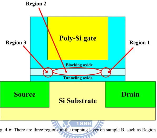
Fig. 4-6: There are three regions in the trapping layer on sample B, such as Region 1 “above drain junction”, Region 2 “above channel center”, and Region 3 “above source junction”………...72 Fig. 4-7: Id-Vg curves of sample C during the operations.
1st state: (Vg = -14V, Vd = 0V, Vs = 0V, for 0.1sec)
2nd state: 1st state + (Vg = 0V, Vd = +10V, Vs = 0V, for 0.1sec)
3rd state: 2nd state + (Vg = +14V, Vd = 0V, Vs = 0V, for 0.1sec)
4th state: 3rd state + (Vg = 0V, Vd = +10V, Vs = 0V, for 0.1sec)………..73
Fig. 4-8: There are five regions in the trapping layer on sample A, such as Region 1 “above drain junction”, Region 2 “above channel and near drain junction”, Region 3 “above channel center”, Region 4 “above channel and near source junction”, and Region 5 “above source junction”………74 Fig. 4-9: The Id-Vg characteristics on sample B after applying different voltages with
same pulse width 1ms……….75 Fig. 4-10: The Vt shift after the program operations at different gate voltages with
different pulse widths on sample B………76 Fig. 4-11: The Vt shift after the erase operations at different gate voltages with
different pulse widths on sample B………76 Fig. 4-12: The increase speed of the GIDL current after the program operations at
different gate voltages with different pulse widths on sample B………...77 Fig. 4-13: The decrease speed of the GIDL current after the erase operations at
different gate voltages with different pulse widths on sample B………...77 Fig. 4-14: The V shift after the program operations at different gate voltages with
different pulse widths on sample A………..78 Fig. 4-15: The Vt shift after the erase operations at different gate voltages with
different pulse widths on sample A………78 Fig. 4-16: The increase speed of the GIDL current after the program operations at
different gate voltages with different pulse widths on sample A………...79 Fig. 4-17: The decrease speed of GIDL current after the erase operations at different
gate voltages with different pulse widths on sample A………..79 Fig. 4-18: The retention characteristics of the Vt on sample B at 25℃ and 85℃…...80
Fig. 4-19: The retention characteristics of the GIDL current on sample B at 25℃ and 85℃………80 Fig. 4-20: The retention characteristics of the Vt on sample A at 25℃ and 85℃……81
Fig. 4-21: The retention characteristics of the GIDL current on sample A at 25℃…..81 Fig. 4-22: The endurance performance of the Vt on sample A……….82
Fig. 4-23: The endurance performance of the Vt on sample B……….82
Fig. 4-24: The endurance performance of the GIDL current on sample A…………...83 Fig. 4-25: The endurance performance of the GIDL current on sample B…………...83 Fig. 4-26: The simulated structure: the lateral charge position is between 0.18 and
0.21μm; the vertical electric field at program operation is drawn along upper line, and the vertical electric field at erase operation is drawn along lower line………84 Fig. 4-27: The vertical electrical field along X-axis at program operation (gate voltage = -5V, source and drain voltage = 0V)………...85 Fig. 4-28: The vertical electrical field along X-axis at erase operation (drain voltage =
+4V, gate and source voltage = 0V)………...85 Fig. 4-29: The illustration of the stored-charges distribution at the drain side after
program state (d) the 2nd erase state………...86 Fig. 4-30: Disturbance effects of the SAHOS memory for 3-bits operations (a) NOR
array structure (b) voltage of bit line and word line during the operations………...87 Fig. 4-31: Read disturbance characteristics of the Vt shift at Vg = 4V………88
Fig. 4-32: Read disturbance characteristics of the GIDL current at Vg = 4V………..88
Fig. 4-33: Read disturbance characteristics of the Vt shift at Vg = -8V………...89
Fig. 4-34: Read disturbance characteristics of the GIDL current at Vg = -8V……….89
Fig. 4-35: Gate disturbance characteristics of the Vt shift under the program operation.
………..………..90 Fig. 4-36: Gate disturbance characteristics of the GIDL current under the program operation……….90 Fig. 4-37: Gate disturbance characteristics of the Vt shift under the erase operation..91
Fig. 4-38: Gate disturbance characteristics of the GIDL current under the erase operation………...……….….91 Fig. 4-39: Drain disturbance characteristics of the Vt shift………..92
Chapter 1
Introduction
1-1 Evolution of Non-volatile Memory
Since the millennium, people’s daily life habit has been changed by various kinds of portable electronic products, such as notebook computer, digital camera, MP3 player, personal digital assistant(PDA), USB, iPod…and so on [1]. The memory devices need to be adopted into all of these electronic products to make them work for different functions. These memories can be divided into volatile memory and non-volatile memory. The use of non-volatile memory (NVM) is to remain the storage data for a long time without power supply, and then portable electronic products can work just by battery due to low power consumption of non-volatile memory.
Non-volatile memories are mainly classified into non-charge-based memory and charge-based memory. The typical charge-based memory is the so called flash memory. There are three types of flash memory including the floating gate (FG) type, SONOS (Silicon/Oxide/Nitride/Oxide/Silicon) type, and nano-crystal type. The mainstream of NVM nowadays is floating gate (FG) type. Some non-charge-based memories have been in small volume production, such as magnetroresistive random access memory (MRAM) [2-3]. The production technologies of ferroelectric random access memory (FeRAM) [4-5] and phase change random access memory (PCRAM) [6-7] are still under development. A novel resistive random access memory (RRAM) attracts much more attention recently [8-12]. All types of flash memories and non-charge-based memories are introduced in detail in the following section.
Smart system must have larger brains which include both sophisticated functions (code storage) and more memory capacity (data storage). These characteristics can be served by two types of flash memories. The NOR-type memory has fast and random access capability for the code storage, and the NAND-type memory has the page access architecture for date storage [13].
1-1-1 Floating Gate Non-volatile Memory
Before the floating gate (FG) non-volatile memory, the magnetic-core memory [14] has a lot of issues, such as large volume, high power consumption, and high cost. Therefore, new kind of memory needs to be invented to replace the magnetic-core memory. In 1967, the first floating gate non-volatile memory was invented by D. Kahng and S. M Sze at Bell Labs [15]. As shown in Fig. 1-1, the stacked-gate FG non-volatile memory structure is mainly used as embedded memories for portable electronics. Nowadays, the main products of the non-volatile memory market still adopt the poly-silicon floating gate structure.
However, as scaling down the device size, the conventional FG memories encounter several limitations [16-18]. First, it is difficult to reduce the operation voltage of FG NVMs because the read and program/erase (P/E) speed in the FG non-volatile memory is related to the operation voltage. Unfortunately, the high operation voltage would result in high power consumption. Second, the thickness of tunneling oxide would be thinner than 4~5 nm while scaling down the channel length. Then, the charges stored in the FG would be easy to leak through any defect in the tunneling oxide to the silicon substrate, and the degradation of retention characteristic of FG memory occurs. Moreover, endurance and disturbance characteristics of the FG memory will degrade by some reliability issues such as stress-induced leakage current improvement and tunneling oxide breakdown while scaling the tunneling oxide
thickness. However, thick tunneling oxide will slow down the operation speed, so there is a trade-off between reliability and speed for designing the thickness of tunneling oxide.
Therefore, to overcome the scaling limits of the conventional FG structure, some structures have been suggested by the International Technology Roadmap for Semiconductors (ITRS) including SONOS (Silicon/Oxide/Nitride/Oxide/ Silicon) type and nano-crystal type [19].
1-1-2 SONOS Non-volatile Memory
In 1969, the predecessor of SONOS type non-volatile memory were invented which is p-channel metal-nitride-oxide-silicon (MNOS) structures with 5nm thick silicon dioxide as tunneling layer, 50 nm silicon nitride as charge trapping layer, and a gate electrode sputtered by Al [20-21]. Because charges stored in the nitride layer of the MNOS memory are easy to leak into metal gate, the retention characteristic is poor. The solution to improve the retention characteristic is adding a blocking oxide between the metal gate and the nitride trapping layer. Therefore, the SONOS type non-volatile memory was invented.
In the recent 10 years, a lot of SONOS type flash memory papers have been published [18-19, 22-23]. As shown in Fig. 1-2, the basic structure of SONOS non-volatile memory which stores charges in discrete traps of the silicon nitride layer show better retention and endurance characteristics. Today, it’s the most promising candidate to replace the traditional FG non-volatile memory and have compatibility with standard CMOS technology. The tunneling oxide thickness can be decreased because the stored charges are localized in nitride trapping layer. When defect is generated in the tunneling oxide, only the charges stored near the defect can leak through the tunneling oxide. Therefore, the reliability of SONOS type memory can be
improved while comparing with the FG memory. Moreover, the dielectric constant of silicon nitride is double higher than silicon dioxide, so the vertical electric field will increase in tunneling oxide. The higher vertical electric field results in the improvement of Fowler-Nordheim (FN) P/E speed and the reduction of operation voltage.
However, there are many issues exhibited in SONOS type memory. First, to achieve lower power consumption, the operation voltages need to be reduced. Second, the “charge migration” is a big issue [24]. The charges stored in trapping size may move to the neighboring trapping site. For example, the vertical migration of trapping electrons occurs as Si3N4 is used as trapping layer, and the lateral migration of
trapping electrons occurs as HfO2 is used as trapping layer [24]. Third, tunneling
oxide will be degraded by Channel-Hot-Electron (CHE) programming which accompanies the degradation of endurance performance. The fourth one, gate and drain disturbance may cause movement of stored charge. Last, erase saturation must be concerned [25].
Recently, as a result of those issues existed in the simple SONOS memory, some advanced SONOS type memories such as TaN/AlO/SiN/Oxide/Si (TANOS) [26] and bandgap engineered SONOS (BE-SONOS) [27-28] have been proposed to improve the P/E speed and/or the retention characteristics. First, take a look at TANOS structure, aluminum oxide as blocking oxide layer is a high-κ material. Due to the low gate coupling rate of the conventional SONOS memories, thin tunneling oxide is required to improve P/E speed, but thin tunneling oxide will lead to poor retention characteristic because of charge leakage path formed in tunneling oxide. Using aluminum oxide to replace silicon dioxide as blocking layer, the high gate coupling rate results in higher P/E speed, and maintains the thicker tunneling oxide to preserve good retention characteristics. On the other hand, the traditional n+ poly-Si
gate is replaced by TaN metal gate. Due to the higher work function of TaN metal, the unwanted backward FN tunneling current of electron from top gate can be reduced [29]. For the BE-SONOS, the tunneling oxide is replaced by an ONO (oxide/nitride/oxide) structure which brings about more holes tunneling current at high electric field during erase operation due to the band offset [27]. On the other hand, the thick ONO layer can prevent direct tunneling of holes from substrate at low electric field, so the retention characteristic can be improved by suppressing charge loss [27].
1-1-3 Nano-crystal Non-volatile Memory
Recently, non-volatile memory with nano-crystals has attracted a lot of attention due to its potential for next generation non-volatile memory. As shown in Fig. 1-3, charges are stored in isolated nano-crystals or nano-dots embedded in the trapping layer. Each nano-crystal can store few electrons and then affect the conductivity of channel to cause threshold voltage shift. There are many advantages of nano-crystal NVMs. First, compared to the structure of the SONOS type memory, the lateral migration of stored charges can be suppressed by the dielectric isolation between nano-crystals. It represents better retention characteristics than the SONOS type memory. Second, just few stored charges will leak through the leaky paths formed in the tunneling layer nearby the nano-crystal, and most of the stored charges can remain in the isolated nano-crystals. Therefore, compared to conventional FG memory devices, nano-crystals NVMs can decrease the thickness of the tunneling layer, and then improve the P/E speed or suppress the operation voltage to obtain low power consumption. Third, the vertical electric field between gate and substrate across nano-crystals will increase, and the work function of nano-crystal can be designed for optimizing the device characteristics [30-33]. Last, nano-crystal devices have the
capability of storing two bits of information.
Some possible scaling limits of nano-crystal device have been proposed. When the nano-crystal non-volatile memory device scales down to sub-65nm node, uniform distribution, high density, and small size of nano-crystal is needed. However, the small nano-crystal (< 5nm in diameter) will decrease the trapping efficiency during program operation due to coulomb blockade and quantum confinement effects [34-35]. Consequently, small nano-crystal results in the small memory window. Therefore, the scaling limit for nano-crystal device depends on how small nano-crystals can be made as well as the means to uniformly deposit them.
1-1-4 Non-charge-based Non-volatile Memory
While scaling down the flash memory device, there are some issues need to be conquered, such as low program/erase speed, poor retention time, and high operation voltage [36]. Therefore, non-charge-based NVMs attract significant attention, especial the RRAMs. The resistive switching phenomenon is the change of the resistance of the metal-insulator-metal (MIM) memory cell [37]. Generally, an initial electroforming step is required to apply at fresh samples, and then the system can be switched between a conductive ON-state and a less conductive OFF-state [37]. Resistance switching phenomenon could be divided into unipolar and bipolar systems. Unipolar means the operation of switching is independent on the polarity of the voltage and current signal. In unipolar system, the high-resistance state (OFF) is switched (“ON”) into the low-resistance state (ON) by a threshold voltage and the compliance current. On the other hand, the unipolar system in its low-resistance state (ON) is switched (“OFF”) into the high-resistance state (OFF) by a higher current and a voltage below the set voltage. In contrast, the bipolar system is which the set to the ON state occurs at one voltage polarity, and the reset to the OFF state take place on
reversed voltage polarity [37].
Although RRAM has potential to further scale down than flash memory, RRAM also has a lot of issues required to be resolved. The current issues for RRAM are operation variation, current reduction and device yield. Operation variation issues are about the deviation of operation voltage and values of high and low resistance states.
Nowadays, the only method to increase storage information density is to continuously scale-down the flash memory device and realize multi-bit and/or multi-level per memory cell.
1-2 Motivation
Because it is not easy to further scale down memory device size, multi-bit per memory cell becomes the only method to increase storage information capacity. Recently, some researches show that the SONOS type memories have the possibility to realize two bits per cell, and the device characteristics have been demonstrated [38-41]. Because the charge trapping layer of the SONOS type memory can store charges locally, more than one bit data information can be achieved in one memory device. In addition, modulation of the Gate-Induced-Drain-Leakage (GIDL) current has been proposed to increase bit information in a memory cell, and the simulation results are shown in Fig. 1-4 [38]. When the charges are stored in bit 2, the GIDL current significantly increase by six orders on forward read, but the Vt shift is very
small. On the other hand, when the charges are stored in bit 1, the GIDL current doesn’t increase on forward read, but the Vt shift is remarkably large [38].
Therefore, in this thesis, we use Sentaurus-TCAD simulation software to simulate the Id-Vg curves with various charge distributions in the trapping layer. The
aim of this study is to illustrate multi-bit data information in one memory cell.
We have mentioned that the SONOS type non-volatile memory has poor retention and scaling issues. The operation voltage and power consumption are still not low enough. High-relative permittivity (high-κ) charge trapping layers in poly-Si/SiO2/high-κ/SiO2/Si (SOHOS) memory structure are of increasing attention.
High-κ materials as a charge trapping layer have been proposed to replace the nitride layer in the SONOS structure to reduce the total thickness of gate dielectric stack and to improve the P/E speed as a result of high gate coupling to the conductive channel [24, 42–43]. In order to further improve the charge retention characteristics and reduce the thickness of gate dielectric stack, the high-κ materials with a large barrier height have been adopted to replace silicon dioxide as a blocking layer, such as Al2O3
films [44–47].
A high work function metal gate electrode in metal/Al2O3/HfO2/SiO2/Si
(MAHOS) memory has been proposed but only capacitor structure was fabricated and evaluated [47]. The calculated energy band diagram on Al/Al2O3/HfO2/SiO2/p-Si
(solid line) and Al/SiO2/HfO2/SiO2/p-Si (dash line) structures under the P/E mode is
shown in Fig. 1-5 [47]. Under the program operation, electron current (Jelectron) from
the Si substrate can be increased and hole current (Jhole) from the gate electrode can be
reduced by using the high-κ Al2O3 as a blocking oxide. In contrast, under the erase
operation, the Jhole from the Si substrate can be increased and the electron current
from the gate electrode can be reduced [47].
In this work, poly-Si/Al2O3/HfO2/SiO2/Si (SAHOS) non-volatile memory
devices are fabricated to demonstrate the multi-bit per cell operation predicted by the TCAD simulation. We replace metal gate by poly-Si gate to have better feasibility with standard CMOS integration process. Poly-Si gate has self-alignment feature to form source and drain region, and it is important for scaling down device size and
increasing device density. Since the charge trapping layer HfO2 film of SAHOS
memory can store charges locally, this SAHOS memory has potential to realize multi-bit per cell. Combined with the simulation results in this thesis, we demonstrated 8 states of 3 bits information in this SAHOS memory successfully and clearly point out the stored-charge positions.
1-3 Thesis Organization
This thesis is divided into five chapters and the contents of each chapter are described as follows.
In chapter 1, the evolution of non-volatile memory has been reviewed, and various kinds of the memory structure have been compared. Accordingly, we choose SAHOS type memory as the research target to study the changes of Id-Vg
characteristics by varying the stored charge positions.
In chapter 2, experimental procedure will be described. The device structure parameters and physical models used in the numerical simulation are shown clearly. The fabrication process of the 2μm gate length poly-Si/Al2O3/HfO2/SiO2/Si (SAHOS)
non-volatile memory will be illustrated. In addition, the measurement techniques of electrical characteristics are described.
In chapter 3, we use the simulation tool of Sentaurus-TCAD to study the Id-Vg
characteristics to study the effects of the position of the stored charges. The charges are located in trapping layer with different lateral positions such as above channel center, above channel and near drain junction, above channel and next to drain junction, above drain and next to drain junction, and above drain and away drain junction.
memory fabricated in chapter 2 will be discussed firstly. We will show that the SAHOS flash memory can store 3 bits data information in one memory cell. The threshold voltage (Vt) can shift with large memory window of 7V. Moreover, the Vt
modulation presents good retention of nearly no charge loss after 105 sec and high endurance of 22% degradation after 105 P/E cycles. The GIDL current can be modulated by about two orders of magnitude, but it shows poor retention and poor endurance. We will discuss the possible reasons for the poor retention and endurance performance. Last, we demonstrate the disturbance effect when this memory device is implemented by the NOR array architecture.
Fig. 1-1: Basic concept of floating gate (FG) non-volatile memory.
Fig. 1-3: Basic concept of nano-crystal non-volatile memory.
Fig. 1-4: (a) 2D schematic cross-section of the dual-bit FinFET SONOS NVM cell. (b) Simulated IDS-VGS characteristics show that VT and GIDL can be used to
distinguish the state of Bit 1 and Bit 2. In this figure, ‘0’ (‘1’) refers to the programmed (erased) state [38].
Fig. 1-5: Schematic energy band diagrams of Al/Al2O3/HfO2/SiO2/p-Si (solid line)
and Al/SiO2/HfO2/SiO2/p-Si (dash line) memory structures under (a)
Chapter 2
Experimental Procedure
2-1 Simulation Method
2-1-1 Device Structure
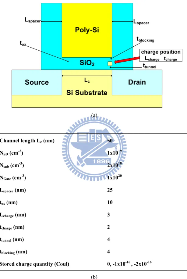
To study the effects of the stored-charge distribution on device characteristics in non-volatile memory, Sentaurus-TCAD tool was used. The device structure was defined by the device simulator DEVISE. In this work, both long channel and short channel devices were studied. Then, the position of the stored-charge was varied relative to the source and drain metallurgic junction position.
The 2-D long channel non-volatile memory structure is shown in Fig. 2-1. The fixed device parameters includes channel width = 1μm, source and drain doping concentration NSD = 5x1019cm-3, substrate doping concentration Nsub= 5x1016cm-3,
poly-Si gate doping concentration NGate = 1x1020cm-3, spacer length Lspacer = 50nm,
gate oxide thickness tox = 12nm, length of the charge storage region Lcharge = 30nm,
thickness of the charge storage region tcharge = 3nm, tunneling oxide thickness ttunnel
=4nm, blocking oxide thickness tblocking = 5nm, and stored-charge quantity = 0 or
-1x10-15Coul. The varied parameters are channel length (Lc), gate to S/D overlap
length (Lol), and stored-charge position. The gate length is fixed at 0.4μm. Therefore,
the overlap length Lol is 50nm as Lc=0.3μm and 0nm as Lc=0.4μm. Five different
stored-charge positions were considered. They are above channel center, above channel and 30nm away from drain junction, above channel and next to drain junction, above drain and next to drain junction, and above drain and 30nm away from drain
junction.
The 2-D short channel non-volatile memory structure is shown in Fig. 2-2. The stored-charge position is defined as silicon, and the spacer is defined as SiO2. The
fixed device parameters includes channel length = 50nm, channel width = 1μm, source and drain doping concentration NSD = 1x1019cm-3, substrate doping
concentration Nsub= 2x1018cm-3, poly-Si gate doping concentration NGate = 1x1020cm-3,
spacer length Lspacer = 25nm, gate oxide thickness tox = 10nm, length of the charge
storage region Lcharge = 3nm, thickness of the charge storage region tcharge = 2nm,
tunneling oxide thickness ttunnel = 4nm, blocking oxide thickness tblocking = 4nm, and
stored charge quantity = 0, -1x10-16, or -2x10-16Coul. The varied device parameter is stored-charge position. Four different stored-charge positions were considered. They are above channel center, above channel and 3nm away from drain junction, above channel and next to drain junction, and above drain and next to drain junction.
2-1-2 Physical Models
DESSIS in Sentaurus-TCAD was used to declare physical models and physical parameters, and to simulate electrical characteristics. Mobility model, bandgap narrowing model, recombination model, and band-to-band tunneling model were included [48]. There are three components used in mobility model. “Doping Dependence” is the first one, and it means the mobility would degrade as doping concentration increase. “High Field Saturation” is the second one, and it means the mobility would be saturated at high electric field. “Enormal” is the last one, and it means the mobility would be affected by the vertical electric field. For recombination model, doping-dependent SRH recombination model is adopted. Recombination through deep levels in the gap is usually labeled as Shockley–Read–Hall (SRH) recombination. Phonon-assisted band-to-band tunneling cannot be neglected in steep
pn-junctions or in high normal electric fields of MOS structures [48].
2-2 Device Fabrication
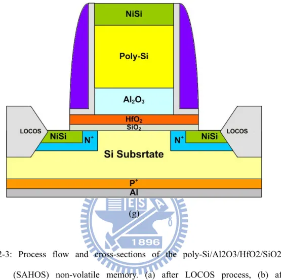
Fig. 2-3 shows the main process flow of the poly-Si/Al2O3/HfO2/SiO2/Si
(SAHOS) non-volatile memory. The devices were fabricated on a 6” p-type Si wafer. At beginning, dry oxide was thermally grown to 35 nm thick in a lateral furnace system. Then, BF2+ ions were implanted into wafer backside at 60 KeV to a dose of
5x1015 cm-2. Zero marks were patterned by optical lithography and plasma etching. In lateral low pressure chemical vapor deposition (LPCVD) system, Si3N4 was deposited
to 150 nm thick. Then, device active regions were patterned, and the Si3N4 and SiO2
layers were etched by plasma etching system of model TEL5000. BF2+ ions were
implanted at 60 KeV to a dose of 2x1013 cm-2 to form the p-type channel stop. The wet oxide of 550nm thick was thermally grown in a lateral furnace, and then wafers were dipped in hot H3PO4 and dilute HF solutions sequentially to remove Si3N4 and
SiO2, respectively. To finish the LOCOS (local oxidation of Si) isolation structure, the
final step is that a wet oxide of 30nm thick was grown in a lateral furnace, and then wafers were dipped in dilute HF solutions to remove oxide. Fig. 2-3(a) shows the LOCOS structure of the device.
After LOCOS isolation process, the tunneling oxide was thermally grown to 4 nm thick in a vertical furnace system. Next, a 5nm thick HfO2 was deposited as
trapping layer in a clustered ALD system and a 20nm thick Al2O3 was deposited as
blocking oxide in the same ALD system followed by a deposition of 150 nm thick LPCVD amorphous-Si gate in a LPCVD system. Then, the amorphous-Si gate was doped with BF2+ at 40KeV to a dose of 5x1015cm-2. After that, gate dopant activation
the amorphous-Si was turned into poly-Si simultaneously. Then, TEOS oxide with a thickness of 100nm as hard mask was deposited on the poly-Si film to avoid unwanted anti-doping during n+ S/D ion implantation. The gate pattern was transferred from i-line photo resist to the TEOS layer by dry etching, and then the remaining etching steps were carried out with the TEOS layer as hard mask. The etching process stopped at the trapping layer. After gate patterning, the schematic cross-sectional structure is shown in Fig. 2-3(b).
Afterwards, the spacer composed of 10 nm SiOX and 50 nm SiNX was formed
as shown in Fig. 2-3(c). Next, P31+ ions were implanted into the S/D region at 20 KeV
to a dose of 5x1015 cm-2 as shown in Fig. 2-4(d). Then the S/D dopants were activated at 900 °C for 20 sec, 60 sec or 180 sec in nitrogen ambient as shown in Fig. 2-3(e). The gate hard mask and native oxide on the S/D region were removed by dipping in dilute HF solution. A 25 nm thick Ni film was deposited by e-gun evaporation followed by a two-step Ni-salicide process [49]. The first step is to form Ni2Si phase,
so the annealing process is executed at 300℃ for 45 minutes in vacuum system. The unreacted Ni was removed by H2SO4/H2O2 = 3:1 solution. The second step is to
transform the Ni2Si phase to the NiSi phase, and the annealing was executed at 600℃
for 30 seconds. After the two-step Ni-salicide process, the S/D region and gate electrode became silicide structure as shown in Fig. 2-3(f). Finally, the poly-Si at backside of the substrate was removed by the HF:HNO3:CH3COOH = 6:20:7 solution
and the oxide was removed by dilute HF solution followed by a deposition of 300nm thick Al film as back electrode of the devices which is shown in Fig. 2-3(g). Table 2-1 summarizes the split conditions used in this thesis.
2-3 Electrical Characterization Techniques
To characterize the SAHOS non-volatile flash memory fabricated in this thesis, several measurements were carried out. We used Agilent 4156C to measure the static current-voltage (I-V) characteristics of the memory device. An Agilent 41501A pulse generation expander was utilized to generate pulse signals during program and erase operations. The substrate terminal of devices was always biased at 0V.
There are many ways to determine the threshold voltage (Vt) which is the most
important parameter of non-volatile memory devices. In this thesis, the method to determinate the threshold voltage is constant drain current method, and this technique is usually adopted in non-volatile memory devices. The gate voltage at a constant drain currentvalue is taken as the threshold voltage. The threshold current value is 100 μA at the drain voltage 1V for sample A, and 1μA at the drain voltage 1V for sample B and sample C. During I-V measurement, the range of gate voltage sweeping should be carefully controlled. If the sweeping range is too large, the unexpected Vt
shift may occur during measurement. Before establishing the characteristics of memory device, the Id-Vg curve should be recorded repeatedly to make sure Vt
stability.
In this thesis, gate-induced drain leakage (GIDL) can be modulated, so that the GIDL can be used to store information. The off current (GIDL) is measured at constant gate voltages of -5V, -7V or -8V as the drain voltage is fixed at +1V.
Because the information can be stored by Vt modulation or off current (GIDL)
modulation separately in this thesis, various memory characteristics are need to be defined and measured respectively. The definition of memory characteristics and methods to measure these characteristics are described as follows.
2-3-1 P/E speed and memory window
(A) Vt modulationVt should be measured as quickly as possible after each program or erase
operation at different gate biases and different pulse widths so that we can obtain the characteristics of P/E speed. The “Vt shift” is defined as the difference of Vt after each
program or erase operation. Before applying another P/E signal, it is essential to return Vt to the same state. For example, before measuring program speed by applying
different pulse widths, the device must be erased to the same Vt. The memory window
is defined as the Vt difference between program state and erase state. During program
and erase operations, both source and drain terminals were biased at 0V, because the charge injection is performed by Fowler-Nordheim (FN) tunneling in this work. (B) GIDL modulation
To characterize the P/E speed, off current (GIDL) was measured after each program or erase operation at different P/E conditions. The bias condition which would increase and decrease the GIDL current is defined as program and erase condition, respectively. The device could be programmed by a negative gate bias, and both source and drain terminals were biased at 0V. On the other hand, the device could be erased by applying a high drain voltage, and both gate and source terminals were biased at 0V. When measuring P/E speed, the GIDL currents were recorded as a function of gate bias after applying different P/E pulses. Before applying another P/E pulse, it is essential to return the GIDL current to the same value by applying a suitable bias condition. Then, the memory window is defined as the difference of GIDL current between program state and erase state.
2-3-2 Retention
for a long time. This means the loss rate of the stored charge need to be as slow as possible.
Generally, retention performance is evaluated as the variation of both program state and erase state as a function of storage time at specified storage temperature. But, in this study, the change of erase state, both Vt and GIDL, as time goes by is so small,
that it can be neglected. To evaluate the retention performance of the program state, the Vt shift and the change of GIDL were recorded as a function of time. In addition, a
small Vg sweeping range should be used to detect the Vt to prevent unwanted Vt shift
during measurement. The ten year residual memory window can be obtained by extrapolation.
2-3-3 Endurance
Endurance is the number of the P/E operation cycles that the memory device can operate without breakdown or vanishing memory window.
(A) Vt modulation
The Vt on program state and erase state were recorded during sequential P/E
cycles. The sequential pulse signals with fixed pulse width and rise/fall time were pulsed into memory devices to establish the endurance characteristics. In this work, 104 P/E cycles were measured on sample A, and 105 P/E cycles were measured on sample B.
(B) GIDL modulation
The GIDL on program state and erase state were recorded during sequential P/E cycles. The sequential pulse signals with fixed pulse width and rise/fall time were pulsed into memory devices to establish the endurance characteristics. In this work, 200 P/E cycles were measured on both sample A and B.
2-3-4 Disturbance
As the result of sharing the same word line and bit line in a memory array, the disturbance problems occur. Generally speaking, the main voltage disturbance on flash memory can be divided into “read disturbance”, “gate disturbance”, and “drain disturbance”. First, when a memory cell operates at read procedure, the read disturbance is defined as the change of the values of Vt and GIDL in this work.
Second, when the selected memory cell is operating at high gate voltage, the other unselected memory cells sharing the same word line may exhibit the variation of Vt or
GIDL, and this phenomenon is called the gate disturbance. Last, when the selected memory cell is operating at high drain voltage bias, the other unselected memory cells sharing the same bit line may exhibit the variations of Vt or GIDL, and this
phenomenon is called the drain disturbance. While measuring the disturbance characteristics, we apply the specific stress conditions to the memory device, and the I-V characteristics were measured at specific times.
Table 2-1: Process conditions of the SAHOS non-volatile memory device fabricated in this thesis.
Sample S/D dopant activation at 900℃ S/D junction overlap with poly-Si gate
A 20s No
B 60s Yes
(a) Channel length Lc (μm) 0.3 0.4 NSD (cm-3) 5x10¹⁹ Nsub (cm-3) 5x10¹⁶ NGate (cm-3) 1x10²⁰ Lspacer (nm) 50 tox (nm) 12 Lcharge (nm) 30 tcharge (nm) 3 ttunnel (nm) 4 tblocking (nm) 5 Lol (nm) 50 0
Stored charge quantity (Coul) 0 or -1x10-15 (b)
(a) Channel length Lc (nm) 50 NSD (cm-3) 1x10¹⁹ Nsub (cm-3) 2x10¹⁸ NGate (cm-3) 1x10²⁰ Lspacer (nm) 25 tox (nm) 10 Lcharge (nm) 3 tcharge (nm) 2 ttunnel (nm) 4 tblocking (nm) 4
Stored charge quantity (Coul) 0, -1x10-16 , -2x10-16 (b)
(a)
(c)
(e)
(g)
Fig. 2-3: Process flow and cross-sections of the poly-Si/Al2O3/HfO2/SiO2/Si (SAHOS) non-volatile memory. (a) after LOCOS process, (b) after dielectric stack deposition and gate patterning, (c) after spacer formation, (d) after S/D ion implantation, (e) after S/D activation, (f) after gate hard mask removal and silicide formation, (g) after back electrode formation.
Chapter 3
Simulation Results of Stored Charge
Distribution on Device Characteristics
3-1 Introduction
As non-volatile memory scaling down, the conventional NVMs encounter many challenges to be overcome. Therefore, the memory device which can store more than one bit per cell becomes the promising device for further improving storage information capacity. The SONOS type memory has potential to realize two bits per cell, and the device characteristics with two bits per cell have been published [38-41]. Some papers have proposed that the modulation of the Gate-Induced-Drain-Leakage (GIDL) current is a potential way to distinguish a bit in the two-bit memory device [38-41]. The GIDL has been investigated since 1987 by J. Chen et al. [50]. Fig. 3-1 shows that the deep-depletion region is formed in the gate-to-drain overlap region, and the band-to-band tunneling mechanism of carrier occurs [50]. On one hand, the electrons at the valence-band tunnel into the conduction band and then are collected at the drain. On the other hand, the holes generated at the deep-depletion region flow to the substrate simultaneously [50].
The modulation of the Vt and the modulation of the GIDL are related to the
stored-charge positions. Therefore, in this chapter, the effects of stored-charge distribution on device characteristics will be investigated by simulation tool at first.
3-2 Long Channel SONOS type NVM
3-2-1 Overlap between S/D and gate
The simulation parameters have already been declared in chapter 2. In the structure of the device with channel length Lc = 0.3 μm, the gate overlap with the
source and drain (S/D) region by 50nm. The center position of the channel is defined as the origin of the X-axis. The stored-charges at the trapping layer have five different horizontal positions: Position 1 “above channel center”, Position 2 “above channel and 30nm away from drain junction”, Position 3 “above channel and next to drain junction”, Position 4 “above drain and next to drain junction”, Position 5 “above drain and 30nm away from drain junction”. These five positions are indicated in Fig. 3-2. The Id-Vg characteristics with stored-charges at various positions were simulated and
discussed as following. In order to investigate how various charge storage positions can affect the carrier barrier of the channel, the conduction band energy of the channel is discussed later.
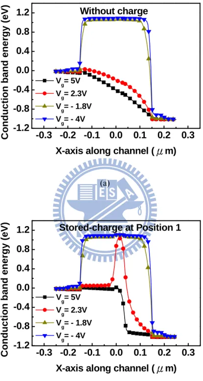
First, compared with the non-charge-stored case, the Id-Vg characteristics with
stored-charges at Position 1 show higher Vt. The whole subthresthold curve was
moved to the right as shown in Fig. 3-2 (a). The negative charges stored at the center of the trapping layer result in a raise of the electron barrier of the channel region, and the conduction band energy diagram is shown in Fig. 3-3. The conduction band energy diagram was drawn along the X-axis within the channel which is 1 nm below the interface which is between the Si substrate and the tunneling oxide. Second, compared with the non-charge-stored case, the Id-Vg characteristics with charges at
Position 2 show higher Vt, but only the upper half subthresthold curve was moved to
the right as shown in Fig 3-2 (b). Next, Fig. 3-2 (c) shows the Id-Vg characteristics
Because the charges storage position is next to the drain junction, it can enhance the vertical electric field between the gate and the drain and then result in larger GIDL. Next, the charges are stored at Position 4 as shown in Fig.3-2 (d). Fig. 3-2 (d) and Fig. 3-2 (c) have similar characteristics as a result of the same physical mechanism. Finally, when the charges are stored at Position 5 as shown in Fig. 3-2 (e), there is no difference compared to the non-charge-stored case.
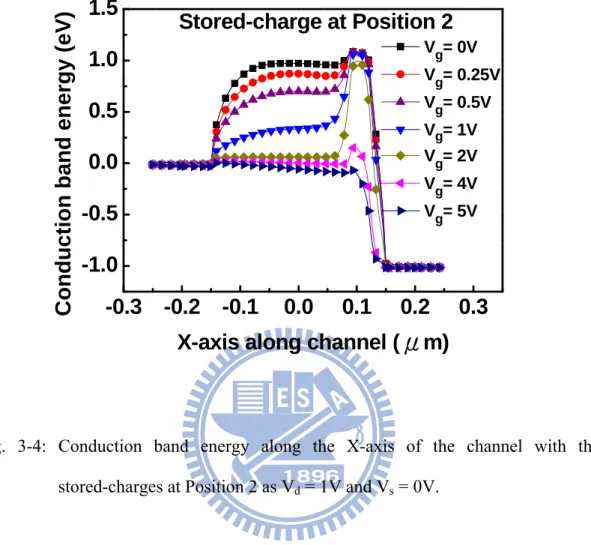
When the charges are at Position 2, the Id-Vg characteristics attract additional
attention. Fig. 3-4 shows the conduction band energy along the X-axis of the channel with the stored-charges at Position 2 as Vd = +1V and Vs = 0V. From Fig. 3-4, the
electron barrier at Vg = 0V with charges at Position 2 is insignificant compared to the
electron barrier of whole channel region. The height of the electron barrier with stored-charges is dragged down by the drain voltage so that the lower half subthreshold curve could keep. When the gate voltage increases to +2V, the electron barrier of channel center decreases apparently. However, the electron barrier with stored-charges decreases much slower than that of channel center, so it can’t allow complete electron conduction. Therefore, the upper half subthreshold curve was moved to the right side.
In summary, placing charges at the above-mentioned charge storage positions can result in the movement of the whole subthreshold curve, the movement of the upper half subthreshold curve, or the increase of the GIDL current. Table 3-1 summarizes the effects of the stored-charge distribution on the device characteristics for the Lc = 0.3 μm long channel device.
3-2-2 Non-overlap between S/D and gate
As mentioned in chapter 2, in the structure of the device with channel length Lc = 0.4 μm, the gate does not overlap with the S/D region. In the trapping layer, the
stored-charges can be placed at four different positions: Position 1 “above channel center”, Position 2 “above channel and 30nm away from drain junction”, Position 3 “above channel and next to drain junction”, Position 4 “above drain and next to drain junction”, as shown in Fig. 3-5. The Id-Vg characteristics with stored-charges at
various positions are also shown in Fig. 3-5. The non-overlap structure and the overlap structure have the similar Id-Vg characteristics. It confirms that the effects of
stored-charge distribution on device characteristics are according to the relative position between the S/D junction and the stored-charge position, but not according to the overlap between the S/D region and the gate.
It is deserved to be mentioned that the GIDL current significantly increase when the charges are stored at Position 4 of this non-overlap structure. This characteristic gives us an idea to extend the trapping layer to the region under the spacer.
3-3 Short Channel SONOS type NVM
From the simulated results of the long channel device, the memory device can store a bit by the modulation of the Vt or the modulation of the GIDL current
respectively. Therefore, it has potential to fabricate a multi-bit memory. Next, the Id-Vg characteristics of the short channel length (50 nm) device with various charge
storage positions are shown in Fig. 3-6.
The charges are located in trapping layer with different lateral positions such as Position 1 “above channel center”, Position 2 “above channel and 3nm away from drain junction”, Position 3 “above channel and next to drain junction”, Position 4 “above drain and next to drain junction”. The Id-Vg characteristics of the short channel
characteristic with the stored-charges at Position 2. In the long channel device, only the upper half subthresold curve shifted to the right. However, in short channel device, the whole subthresold curve shifted to the right. Moreover, in the long channel device, the GIDL current did not increase when the stored-charge at Position 2, but the GIDL current increased slightly in the short channel device.
The GIDL current increases when the charges are stored at Position 4 in the short channel device. This phenomenon also occurs in the long channel device. Therefore, it confirms that fabricating multi-bit memory device by extending trapping layer to the region under the spacer is feasible at both long and short channel device. Table 3-2 summarizes the effects of stored-charge distribution on device characteristics for 50 nm short channel device.
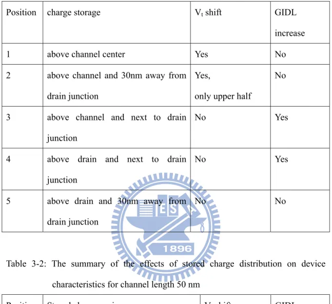
Table 3-1: The summary of the effects of stored-charge distribution on device characteristics for channel length 0.3 μm
Position charge storage Vt shift GIDL
increase
1 above channel center Yes No
2 above channel and 30nm away from drain junction
Yes,
only upper half
No
3 above channel and next to drain junction
No Yes
4 above drain and next to drain junction
No Yes
5 above drain and 30nm away from drain junction
No No
Table 3-2: The summary of the effects of stored charge distribution on device characteristics for channel length 50 nm
Position Stored charge region Vt shift GIDL
increase
1 above channel center Yes No
2 above channel and 3nm away from drain junction
Yes, slightly Yes, slightly
3 above channel and next to drain junction
No Yes
(a) (b)
Fig. 3-1: (a) Physical mechanisms of the GIDL (b) current-voltage characteristics of the GIDL phenomenon [50].
(a) (b) Si Substrate SiO2 Poly-Si Drain Source Charge
Si Substrate
SiO
2Poly-Si
Drain
Source
Charge
-4 -2 0 2 4 6 10-17 10-15 10-13 10-11 10-9 10-7 10-5 10-3 0 Coul -1X10-15 Coul Stored-charge at Position 1 Drain cu rren t (A) Gate voltage (V) -4 -2 0 2 4 6 10-17 10-15 10-13 10-11 10-9 10-7 10-5 10-3 -1X10-15 Coul 0 Coul Stored-charge at Position 2 Drain cu rren t (A) Gate voltage (V)(c) (d)
Si Substrate
SiO
2Poly-Si
Drain
Source
Charge
Si Substrate SiO2 Poly-Si Drain Source Charge -4 -2 0 2 4 6 10-17 10-15 10-13 10-11 10-9 10-7 10-5 10-3 -1X10-15 Coul 0 Coul Stored-charge at Position 3Drain current (A)
Gate voltage (V) -4 -2 0 2 4 6 10-17 10-15 10-13 10-11 10-9 10-7 10-5 10-3 Stored-charge at Position 4 -1X10-15 Coul 0 Coul Drain current (A) Gate voltage (V)
(e)
Fig. 3-2: The Id-Vg characteristics with the stored-charges at various positions for the
long channel 0.3 μm device. (a) Position 1 “above channel center”, (b) Position 2 “above channel and 30nm away from drain junction”, (c) Position 3 “above channel and next to drain junction”, (d) Position 4 “above drain and next to drain junction”, (e) Position 5 “above drain and 30nm away from drain junction”.
Si Substrate
SiO
2Poly-Si
Drain
Source
Charge
-4 -2 0 2 4 6 10-17 10-15 10-13 10-11 10-9 10-7 10-5 10-3 Stored-charge at Position 5 0 Coul -1X10-15 CoulDrain current (A)
-0.3 -0.2 -0.1 0.0 0.1 0.2 0.3 -1.2 -0.8 -0.4 0.0 0.4 0.8 1.2 Without charge C o nduc
tion band ene
rgy
(
e
V)
X-axis along channel (
μ
m)V g= 5V Vg= 2.3V Vg= - 1.8V Vg= - 4V (a) -0.3 -0.2 -0.1 0.0 0.1 0.2 0.3 -1.2 -0.8 -0.4 0.0 0.4 0.8 1.2 Vg= 5V V g= 2.3V V g= - 1.8V Vg= - 4V Stored-charge at Position 1 C o nduc
tion band ene
rgy
(
e
V)
X-axis along channel (
μ
m)(b)
Fig. 3-3: Conduction band energy along the X-axis of the channel (a) without charge (b) stored-charge at Position 1.
-0.3
-0.2
-0.1
0.0
0.1
0.2
0.3
-1.0
-0.5
0.0
0.5
1.0
1.5
Stored-charge at Position 2
Vg= 0V Vg= 0.25V Vg= 0.5V Vg= 1V Vg= 2V Vg= 4V Vg= 5VC
onduc
tion band e
n
er
gy
(e
V)
X-axis along channel (
μ
m)
Fig. 3-4: Conduction band energy along the X-axis of the channel with the stored-charges at Position 2 as Vd = 1V and Vs = 0V.
(a) (b) Si Substrate SiO2 Poly-Si Drain Source Charge
![Fig. 1-5: Schematic energy band diagrams of Al/Al 2 O 3 /HfO 2 /SiO 2 /p-Si (solid line) and Al/SiO 2 /HfO 2 /SiO 2 /p-Si (dash line) memory structures under (a) program and (b) erase modes [47]](https://thumb-ap.123doks.com/thumbv2/9libinfo/8755902.206893/30.892.140.752.139.758/schematic-energy-diagrams-memory-structures-program-erase-modes.webp)