國
立
交
通
大
學
光電工程研究所
碩
士
論
文
直接偵測正交分頻多工多級格式 I/Q 全光升頻系
統
Optical I/Q Up-Conversion for Direct Detection Multi-Level
Format OFDM Systems
研 究 生:翁而咨
指導教授:陳智弘 教授
直接偵測正交分頻多工多級格式 I/Q 全光升頻系統
Optical I/Q Up-Conversion for Direct Detection Multi-Level
Format OFDM Systems
研 究 生:翁而咨 Student:Er-Zih Wong 指導教授:陳智弘 Advisor:Jyehong Chen
國 立 交 通 大 學 光電工程研究所
碩 士 論 文
A Thesis Submitted to Department of Phptonics College of Electrical Engineering and Computer Science
National Chiao Tung University in partial Fulfillment of the Requirements
for the Degree of Master
in Photonics
July 2009
Hsinchu, Taiwan, Republic of China
i
直接偵測多級格式正交多頻分工全光升頻系統
研 究 生: 翁而咨 指導教授: 陳智弘 博士
國立交通大學 電機資訊學院
光電工程研究所
摘要 我們提出了一個新穎的全光升頻直接偵測多級格式正交多頻分 工系統。藉由外接調變器產生單邊帶載子壓制調變來產生全光升頻向 量訊號,此架構不需要電的混波器及能升頻。為了產生 60GHz 的訊號, 我們引進四倍頻的調變技術,並成功地在 60GHz 的免授權 7GHz 頻段 產生 28Gb/s 16-QAM OFDM 訊號。在沒有任何色散補償的狀況下,經 過一百公里的單模光纖傳輸,此訊號幾乎沒有損耗。 除此之外,我們還討論這個架構的不平衡效應,並針對這些問題 提出補償方法來提升訊號品質。造成不平衡的因素包括:振幅不相符、 角度不為直角以及兩路訊號不同步。用 GSOP 校正方法可以成功解決 這些問題。 最後我們討論光的相位雜訊對訊號的影響。當我們的訊號傳輸量 愈大時,光的相位雜訊會對訊號品質造成很大的影響。ii
Optical Up-Conversion for Direct Detection
Multi-Level Format OFDM Systems
Student: Er-Zih Wong Advisor: Dr. Jyehong Chen
Department of Photonics,
National Chiao Tung University
ABSTRACT
We propose a novel all optical up-conversion direct detection OFDM multi-level system. Utilizing an external modulator, we can up-converse vector signals without electrical mixer based on single side band with carrier suppression. In order to generate 60GHz signals without expensive high-speed components, we using frequency quadrupling modulation technique. A record 28-Gb/s 16-QAM OFDM system within 7-GHz license-free band at 60 GHz employing all-optical up-conversion with frequency quintupling is experimentally demonstrated. Negligible penalty is observed following 100-km SMF transmission without any dispersion compensation.
Besides, we also discuss imbalance effects and do compensation to improve signal quality. The imbalance factors include amplitude mismatch, conjugate misalignment and un-synchronization. Utilizing Gram-Schmidt Orthogonal procedure can successfully solve these problems.
Finally, we also do some discussion on phase noise. It affects high data rate signals seriously.
iii Acknowledgements 在研究所的求學過程中,首先感謝我的指導老師 陳智弘教授與 祁甡教授,提供良好的實驗環境以及無私的照顧與指導,使我可以心 無旁騖得完成學業並從中獲得許多收穫與成長。實驗方面特別感謝林 俊廷學長教導我許多實驗方法,並無私的指教以及修正了許多理論概 念以及物理意義,另外感謝施伯宗學長和江文智學長教導我許多實驗 技巧以及引領我解決實驗問題,還有林玉明學長在程式方面提供不少 協助。 接下來要感謝實驗室的夥伴。非常感謝同在這個實驗室的同學們 -陳星宇、葉士愷、黃漢昇以及陳昱宏同學,不僅在實驗上給予協助, 並幫助我解決不少生活上的小問題;在此也要特別感謝熱心幫我處理 許多瑣事的學弟們,彥霖以及立穎,在我忙碌時給予不少協助。還要感 謝平時給我許多鼓勵的好友們,謝謝你們的關心和支持,讓我在受到 挫折時能繼續向上努力。 最後要感謝我的家人,感謝你們的支持與鼓勵,並時時給予溫暖 的關心,讓我無後顧之憂的完成學業。 帶著愉快回憶和滿載的收穫邁向人生的下個旅程,再會了交大! 翁而咨 于 風城 交大 民國九十八年六月
iv CONTENTS English Abstract...i Chinese Abstract... ii Acknowledgements... iii Contents... iv List of Figures...vi Chapter 1 Introduction ... 1
1.1 Review of Radio-over-fiber system ... 1
1.2 Basic modulation schemes ... 3
1.3 Motivation... 4
Chapter 2 The Concept of New Optical Modulation System ... 6
2.1 Preface ... 6
2.2 Mach-Zehnder Modulator (MZM) ... 6
2.3 Single-drive Mach-Zehnder modulator ... 6
2.4 The architecture of ROF system ... 7
2.4.1 Optical transmitter ... 7
2.4.2 Optical signal generations based on LiNbO3 MZM ... 8
2.4.3 Communication channel ... 10
2.4.4 Demodulation of optical millimeter-wave signal ... 11
2.5 The new proposed model of optical modulation system ... 12
Chapter 3 The theoretical calculations of Proposed system ... 14
3.1 Introduce MZM ... 14
3.2 Theoretical calculation of single drive MZM ... 17
3.2.1 Bias at maximum transmission point ... 17
v
3.2.3 Bias at null point ... 19
3.3 Theoretical calculations and simulation results ... 20
3.4 I/Q imbalance ... 28
3.4.1 Preface ... 28
3.4.2 Concept of proposed system ... 29
3.4.3 Amplitude mismatch ... 31
3.4.4 Conjugate misalignment ... 37
3.4.5 Synchronization ... 43
Chapter 4 Experimental demonstration of proposed system ... 46
4.1 preface ... 46
4.2 Comparison of different DD-OFDM modulation scheme ... 46
4.3 Cpncept of proposed system ... 48
4.4 Experimentl results for all optical I/Q up conversion system... 51
4.4.1 Experiment setup ... 51
4.4.2 Optimal condition for RF signals ... 52
4.4.3 Transmission results ... 55
4.5 The infulence of phase noise ... 60
Chapter 5 60GHz system ... 64
5.1 Introduction of frequency quadrupling scheme ... 64
5.2 Concept of the 60GHz system ... 65
5.3 Experimental setup ... 66
5.3.1 Optimal condition for RF signals ... 68
5.4 Experimental results and discussion ... 74
Chapter 6 Conclusion ... 85
vi
Appendix... 88 Vita ... 90
vii
LIST OF FIGURES
Figure 1-1 Basic structure of microwave/millimeter-wave wireless system. …2
Figure 1-2 The Radio-over fiber system. ………3
Figure1-3Comparison of different DD-OFDM modulation shceme. (B: bandwidth of DAC, f0: optical carrier frequency, f0: intermedium frequency)...5
Figure 2-1 (a) and (b) are two schemes of transmitter and (c) is duty cycle of subcarrier biased at different points in the transfer function. (LO: local oscillator).……….7
Figure 2-2 Optical microwave/mm-wave modulation scheme by using MZM..9
Figure 2-3The model of communication channel in a RoF system. …………10
Figure 2-4The model of receiver in a ROF system. ……….11
Figure 2-5 The model of ROF system. ……….11
Figure2-6 Conceptual diagram of optical I/Q up-conversion for direct-detection OFDM signals. ………..13
Figure 3-1 The principle diagram of the optical mm-wave generation using balanced MZM. ……….17
Figure 3-2The different order of Bessel functions vs. m. ………18
Figure 3-3 The different order of Bessel functions vs. m. ………28
Figure 3-4 The concept of proposed system. ………29
Figure 3-5 Imbalance factors of proposed system. ………...30
Figure 3-6 BER and SNR vs. I/Q ratio for simulation single carrier QPSK. ...31
Figure 3-7 Constellations for simulation QPSK amplitude mismatch w/ and w/o correction. (a) I/Q=8dB w/o correction (b) I/Q=8dB w/ correction (c) I/Q=4dB w/o correction (d) I/Q=4dB w/ correction (e) I/Q=0dB w/o correction (f) I/Q=0dB w/ correction. ……….32
viii
Figure 3-8 BER vs. I/Q ratio(Amplitude Mismatch) for experimental single carrier QPSK. ………..………33 Figure 3-9 Constellations for experimental QPSK amplitude mismatch w/ and w/o correction. (a) I/Q=8dB w/o correction (b) I/Q=8dB w/ correction (c) I/Q=4dB w/o correction (d) I/Q=4dB w/ correction (e) I/Q=0dB w/o correction (f) I/Q=0dB w/ correction. ………..34 Figure3-10 BER and SNR vs. I/Q ratio for simulation single carrier
16-QAM ………..35 Figure 3-11 Constellations for simulation 16QAM amplitude mismatch w/ and
w/o correction. (a) I/Q=8dB w/o correction (b) I/Q=8dB w/ correction (c) I/Q=4dB w/o correction (d) I/Q=4dB w/ correction (e) I/Q=0dB w/o correction (f) I/Q=0dB w/ correction. …..……36 Figure 3-12 BER and SNR vs. conjugate misalignment for simulation single
carrier QPSK. ………...………37 Figure 3-13 Constellations for simulation QPSK conjugate misalignment w/
and w/o GSOP. (a) 30° w/o GSOP (b) 30° w/ GSOP (c) 10° w/o GSOP (d)10° w/ GSOP (e) 0° w/o GSOP (f) 0° w/ GSOP. ……..38 Figure 3-14 BER vs. conjugate misalignment for experimental single carrier
QPSK. …..………...39 Figure 3-15 Constellations for experimental QPSK conjugate misalignment w/ and w/o GSOP.(a) 30° w/o GSOP (b) 30° w/ GSOP (c) 10° w/o GSOP (d)10° w/ GSOP (e) 0° w/o GSOP (f) 0° w/ GSOP. .…….40 Figure 3-16 BER and SNR vs. conjugate misalignment for simulation single carrier 16-QAM. ………...41
ix
Figure 3-17Constellations for simulation 16-QAM conjugate misalignment w/ and w/o GSOP. (a) 30° w/o GSOP (b) 30° w/ GSOP (c) 10° w/o GSOP (d)10° w/ GSOP (e) 0° w/o GSOP(f) 0° w/ GSOP. .……..42 Figure 3-18 BER and SNR vs. Time Delay for simulation QPSK. (a)Time delay 50% w/o correction.(b)Time delay 50% with correction. ……..…43 Figure 3-19 BER and SNR vs. Time Delay for experimental QPSK. (a)Time delay 50% w/o correction.(b) Time delay 50% with correction. ...44 Figure 3-20 BER and SNR vs. Time Delay for simulation 16-QAM. (a)Time
delay 50% w/o correction.(b) Time delay 50% with correction. …45 Figure 4-1 Comparison of different DD-OFDM modulation shceme.
(B:bandwidth of DAC, f0: optical carrier frequency, f0:
intermedium frequency). ...47 Figure 4-2 The Concept of All Optical IQ Up Conversion System. ………….50 Figure 4-3 The Experimental Setup of All Optical IQ Up Conversion System. ……….51 Figure 4-4 Optical Spectrum of single carrier QPSK signal.OPR= Pd/Ps(dB), Pd: optical power of data-modulated optical carrier; Ps: optical p o w e r o f 7 . 5 G H z s u b c a r r i e r. O P R =- 4 d B ( b ) O P R =0 d B (c) OPR=4dB. ……….…………..52 Figure 4-5 BER vs. OPR curve for single carrier QPSK signal. ………..53 Figure 4-6 Optical Spectrum of OFDM 16QAM signal.OPR= Pd/Ps(dB), Pd: optical power of data-modulated optical carrier; Ps: optical power of 7.5GHz subcarrier.OPR=5dB (b) OPR=3dB (c) OPR=1dB..…….54 Figure 4-7 BER vs. OPR curve for OFDM 16QAM signal. ………54 Figure 4-8 Electrical Spectrums for Single Carrier QPSK. (a)Tx terminal Electrical Spectrum. (b) Rx terminal Electrical Spectrum. …...55 Figure 4-9 Electrical Spectrum for OFDM 16QAM. (a)Tx terminal Electrical Spectrum.(b)Rx terminal Electrical Spectrum. …...56
x
Figure 4-10 BER-Receiver Power curve for QPSK. ………56 Figure 4-11 Constellations and eye diagrams for single carrier QPSK signals at
P D In p ut Po w er =-1 2. 5 dB m. BT B ( b) 2 5 km ( c) 50 km (d)100km. ………58 Figure 4-12 BER-Receiver Power curve for OFDM 16QAM. ……….59 Figure 4-13 Constellations and eye diagrams for OFDM 16QAM signals at PD
I n p u t P o w e r = - 8 d B m . ( a ) B T B ( b ) 2 5 k m ( c ) 5 0 k m (d)100km. ...60 Figure 4-14 BER and SNR vs. Laser Line-Width for simulation 28Gb/s OFDM 16-QAM. ……..………...61 Figure 4-15 BER curves of 60-GHz 20-Gb/s 16-QM OFDM signals. The
linewidth is 10 MHz. ………62 Figure4-16BER curves of 60-GHz 20-Gb/s 16-QM OFDM signals. The linewidth is 10 KHz. ……….62 Figure5-1 Frequency quadrupling scheme. ….………..64 Figure.5-2 Conceptual diagram of the 60-GHz optical/wireless system using
all-optical up-conversion. ……..……….65 Figure.5-3 Experimental setup for proposed system. ………...66 Figure 5-4.BER vs. OPR for OFDM QPSK. OPR=Pd/Ps(dB). Pd: the optical power of data-modulated optical carrier. Ps: the optical power of un-modulated subcarrier. ……….………...68 Figure 5-5.Optical Spectrums for OFDM QPSK.(a)OPR=3dB (b) OPR=3dB
after 4f-system (c) OPR=0.4dB (d)OPR=0.4dB after 4f-system(e) OPR=-1.4dB (f) OPR=-1.4dB after 4f-system. …………..………69
xi
Figure 5-6.BER vs. OPR for 20Gb/s OFDM 16QAM.OPR=Pd/Ps(dB). Pd: the optical power of data-modulated optical carrier.Ps: the optical power of un-modulated subcarrier. ………...………...70 Figure 5-7.Optical Spectrums for 20Gb/s OFDM 16-QAM. (a)OPR=1dB
(b) OPR=1dB after 4f-system (c) OPR=3dB (d) OPR=3dB after 4f-system(e) OPR=5dB (f) OPR=5dB after 4f-system. …………..71 Figure 5-8.BER vs. OPR for 28Gb/s OFDM 16QAM. OPR=Pd/Ps(dB). Pd: the optical power of data-modulated optical carrier. Ps: the optical power of un-modulated subcarrier. ………...72 Figure 5-9.Optical Spectrums for 28Gb/s OFDM 16-QAM. (a)OPR=0dB
(b) OPR=0dB after 4f-system (c) OPR=4dB (d) OPR=4dB after 4f-system(e) OPR=8dB (f) OPR=8dB after 4f-system. ………….73 Figure 5-10. Electrical Spectrums of QPSK OFDM signals. (a)Tx OFDM and subcarrier electrical spectrum. (b)OFDM electrical spectrum after I/Q modulator.(c)Rx OFDM electrical spectrum. ………….…...74 Figure 5-11. BER curves of the OFDM QPSK signals. ………...74 Figure 5-12 Constellations of QPSK OFDM signals (-11dBm).
(a) BTB before 4f (b) BTB (c) 50km (d) 100km.………...76 Figure 5-13. Electrical Spectrums of 20Gb/s 16-QAM OFDM signals. (a)Tx OFDM and subcarrier electrical spectrum. (b)Rx OFDM electrical spectrum. ………...76 Figure 5-14. BER curves of the 20Gb/s OFDM 16-QAM signals using DFB
xii
Figure 5-15. Constellations of 20Gb/s 16-QAM OFDM signals using DFB Laser (-5dBm). (a) BTB (b) 25km (c) 50km (d) 75km
(e) 100km. ………...78 Figure 5-16. Electrical Spectrums of 20Gb/s 16-QAM OFDM signals with
tunable laser (TL).(a)Tx OFDM and subcarrier electrical spectrum. (b)Rx OFDM electrical spectrum. ………79 Figure 5-17. BER curves of the 20Gb/s OFDM 16-QAM signals using Tunable
Laser. ……….80 Figure 5-18. Constellations of 20Gb/s 16-QAM OFDM signals using Tunable Laser (-5dBm). (a) BTB (b) 25km (c) 50km (d) 100km. ……….81 Figure 5-19. Electrical Spectrums of 28Gb/s 16-QAM OFDM signals with
tunable laser (TL). (a)Tx OFDM and subcarrier electrical spectrum. (b)Rx OFDM electrical spectrum. ……….………...82 Figure 5-20. BER curves of the 28Gb/s OFDM 16-QAM signals using Tunable Laser. ……….82 Figure 5-21. Constellations of 28Gb/s 16-QAM OFDM signals using Tunable Laser (-5 dB m). (a) BTB w/ o E.Q. (b) BTB (c) 50 km (d) 100km. ...84
1
Chapter 1 Introduction 1.1 Review of Radio-over-fiber system
There are many applications in microwave band, such as 3G, WiFi (IEEE 80211 b/g/a), and WiMAX are very important for wireless network. The increasing demand for communication has attracted more and more research interests of new transmission systems. Hence, to develop higher frequency microwave, even millimeter-wave is a important issue now. Either employing multilevel modulation schemes or extending the carrier frequency into millimeter-wave band can achieve higher data rate. Especially, the 7-GHz license-free spectrum at 60 GHz is the most promising solution to wireless gigabit service [1-3]. However, 60-GHz millimeter-wave has very high atmospheric loss and the access coverage is limited to relatively short range.
Because the higher frequency millimeter-wave signals have smaller coverage area, we have to set a lot of base stations to deliver millimeter-wave signals as shown in Fig. 1-1. In order to reduce the system costs and base stations (BSs) we utilize a highly dense central station (CS) equipped with optical and mm-wave components. Using fiber transmission medium is one of the best solutions because of unlimited bandwidth and low transmission loss of optical fiber, radio-over-fiber (RoF) technology is a promising solution to provide broadband service, wide coverage, and mobility.
2
Figure 1-1 Basic structure of microwave/millimeter-wave wireless system.
Broadband wireless communications are shown in Fig. 1-2. ROF technology is a promising solution to provide multi-gigabits/sec service because of using millimeter wave band, and it has wide converge and mobility.On the other hand, due to high tolerance against fiber dispersion and polarization-mode dispersion, orthogonal frequency division multiplexing (OFDM) systems, which have been widely utilized in the current wireless communication, have attracted a lot of attention for optical high-capacity long-haul communication, multimode fiber links, and plastic optical fiber link. Besides, highly spectral efficiency and flexibility of OFDM makes it attractive for narrowband applications beyond the 10-Gb/s regime. Due to orthogonal characteristic of each subcarrier of OFDM signals, compared with single-carrier systems, an OFDM system has better spectral efficiency and can provide higher data rate within the 7-GHz license-free spectrum at 60 GHz.
3
Figure 1-2 The Radio-over fiber system. 1.2 Basic modulation schemes
There are several kind of modulation schemes using an external modulator, such as double-sideband (DSB), single-sideband (SSB), and double-sideband with optical carrier suppression (DSBCS) modulation, and these schemes have already been demonstrated on many publications[1,2,4-8]. Each modulation scheme has its own advantage and disadvantage, respectively. DSB is the most compact system, but it suffers inferior sensitivities due to limited optical modulation index (OMI) [4-6,8], and fading issue because of fiber dispersion [6]. SSB can overcome fading, but it suffers inferior sensitivities as well. Among these modulation schemes, DSBCS modulation has been demonstrated to be effective in the millimeter-wave range with excellent spectral efficiency, a low bandwidth requirement for electrical components, and superior receiver sensitivity following transmission over a long distance [6]. Despite all these advantages, DSBCS schemes can only support on-off keying (OOK) format, but cannot transmit vector modulation formats, such as phase shift keying (PSK), quadrature amplitude modulation (QAM), or OFDM signals, which are of utmost importance for wireless applications.
4
This study proposes a modified single sideband (SSB) modulation scheme with carrier suppression using one MZM. A all optical up-conversion scheme is employed to reduce the requirement of bandwidth of electronic components and use no electrical mixer with noise figure 8 dB, which is an important issue at millimeter-wave RoF systems. Benchmarked against the OOK format, the 14.0625-Gb/s QPSK-OFDM and 28.125-Gb/s 16-QAM-OFDM format has the higher spectral efficiency.
1.3 Motivation
Recently , there several countries has already released the unlicensed spectrum about 7GHz near the 60GHz band . However, the coverage of the 60-GHz wireless signals is limited by the high path and atmospheric losses. To extend the signal coverage, radio-over-fiber (RoF) techniques become a promising solution for broad band wireless access networks. So in this work, we want to propose a new RoF system which has high spectral efficiency and satisfy the 60GHz applications.
Besides, traditional ways to generating SSB signals are shown as inset (i) and (ii) of figure 1-3. However, conventional SSB modulation approaches suffer from inferior sensitivities because the optical modulation index (OMI) is limited. Furthermore, to avoid beat noise after photo detection, an electrical I/Q mixer with a typical noise figure (NF) of more than 8 dB is needed to up-convert OFDM signal to intermedium frequency, which severely hinders implementation of highly spectral efficiency QAM OFDM signal for narrowband applications in the 10-Gb/s regime.
5
Figure1-3 Comparison of different DD-OFDM modulation shceme. (B: bandwidth of DAC, f0: optical carrier frequency, f0: intermedium frequency)
Virtual SSB modulation scheme without electrical I/Q mixer is proposed as shown in inset (ii) of Figure 1-3. The drawback is that half bandwidth of the DAC is wasted to avoid the beat noise interference. In order to improve these problems, we propose a modified SSB modulation.
6
Chapter 2 The concept of new optical modulation system 2.1 Preface
There are three parts in optical communication systems : optical transmitter, communication channel and optical receiver. In this chapter, we will briefly introduce about how these three parts work, and what is the external Mach-Zehnder Modulator (MZM), and how MZM construct a Radio-over-Fiber (RoF) system. In the end, we will propose a new model of the RoF system.
2.2 Mach-Zehnder Modulator (MZM)
Direct modulation and external modulation are two modulations of generated optical signal. When the bit rate of direct modulation signal is above 10 Gb/s, the frequency chirp imposed on signal becomes large enough. Hence, it is difficult to apply direct modulation to generate microwave/mm-wave. However, the bandwidth of signal generated by external modulator can exceed 10 Gb/s. Presently, most RoF systems are using external modulation with Mach-Zehnder modulator (MZM) or Electro-Absorption Modulator (EAM). The most commonly used MZM are based on LiNbO3 (lithium niobate) technology. According to the applied electric field, there are two types of LiNbO3 device : x-cut and z-cut. According to number of electrode, there are two types of LiNbO3 device: dual-drive Mach-Zehnder modulator (DD-MZM) and single-drive Mach-Zehnder modulator (SD-MZM) [6].
2.3 Single-drive Mach-Zehnder modulator
The SD-MZM has two arms and an electrode. The optical phase in each arm can be controlled by changing the voltage applied on the electrode. When the lightwaves are in phase, the modulator is in “on” state. On the other hand, when the lightwaves
7
are in opposite phase, the modulator is in “off ” state, and the lightwave cannot propagate by waveguide for output.
2.4 The architecture of ROF system 2.4.1 Optical transmitter
Figure 2-1(a) and (b) are two schemes of transmitter and (c) is duty cycle of subcarrier biased at different points in the transfer function. (LO: local oscillator)
Optical transmitter consists of optical source, optical modulator, RF signal, electrical mixer, electrical amplifier, etc.. Recently, most RoF systems are using laser as light source. The advantages of laser are compact size, high efficiency, good reliability small emissive area compatible with fiber core dimension, and possibility of direct modulation at relatively high frequency. The modulator is used for converting electrical signal into optical form. Because the external integrated modulator was
8
composed of MZMs, we select MZM as modulator to build the architecture of optical transmitter.
There are two schemes of optical transmitter generated optical signal. One scheme is used two MZM. First MZM generates optical carrier which carried the data. The output optical signal is BB signal. The other MZM generates optical subcarrier which carried the BB signal and then output the RF signal, as shown in Fig. 2-1 (a). The other scheme is used a mixer to get up-converted electrical signal and then send it into a MZM to generate the optical signal, as shown in Fig. 2-1 (b). Fig. 2-1 (c) shows the duty cycle of subcarrier biased at different points in the transfer function.
2.4.2 Optical signal generations based on LiNbO3 MZM
The microwave and mm-wave generations are key techniques in RoF systems. The optical mm-waves using external MZM based on double-sideband (DSB), single-sideband (SSB), and double-sideband with optical carrier suppression (DSBCS) modulation schemes have been demonstrated, as shown in Fig. 2-2. Generated optical signal by setting the bias voltage of MZM at quadrature point, the DSB modulation experiences performance fading problems due to fiber dispersion, resulting in degradation of the receiver sensitivity. When an optical signal is modulated by an electrical RF signal, fiber chromatic dispersion causes the detected RF signal power to have a periodic fading characteristic. The DSB signals can be transmitted over
9
Figure2-2Optical microwave/mm-wave modulation scheme by using MZM.
several kilo-meters. Therefore, the SSB modulation scheme is proposed to overcome fiber dispersion effect. The SSB signal is generated when a phase difference of π/2 is applied between the two RF electrodes of the DD-MZM biased at quadrature point. Although the SSB modulation can reduce the impairment of fiber dispersion, it suffers worse receiver sensitivity due to limited optical modulation index (OMI). The DSBCS modulation is demonstrated optical mm-wave generation using DSBCS modulation. It has no performance fading problem and it also provides the best receiver sensitivity because the OMI is always equal to one. The other advantage is that the bandwidth requirement of the transmitter components is less than DSB and SSB modulation. However, the drawback of the DSBCS modulation is that it can’t support vector
10
signals, such as phase shift keying (PSK), quadrature amplitude modulation (QAM), or OFDM signals, which are of utmost importance in wireless applications.
2.4.3 Communication channel
Figure2-3 The model of communication channel in a RoF system.
Communication channel concludes fiber, optical amplifier, etc.. Presently, most RoF systems are using single-mode fiber (SMF) or dispersion compensated fiber (DCF) as the transmission medium. When the optical signal transmits in optical fiber, dispersion will be happened. DCF is use to compensate dispersion. The transmission distance of any fiber-optic communication system is eventually limited by fiber losses. For long-haul systems, the loss limitation has traditionally been overcome using regenerator witch the optical signal is first converted into an electric current and then regenerated using a transmitter. Such regenerators become quite complex and expensive for WDM lightwave systems. An alternative approach to loss management makes use of optical amplifiers, which amplify the optical signal directly without requiring its conversion to the electric domain [14]. Presently, most RoF systems are using erbium-doped fiber amplifier (EDFA). An optical band-pass filter (OBPF) is necessary to filter out the ASE noise. The model of communication channel is shown in Fig. 2-3.
11
2.4.4 Demodulation of optical millimeter-wave signal
Figure 2-4 The model of receiver in a ROF system.
Optical receiver concludes photo-detector (PD), demodulator, etc.. PD usually consists of the photo diode and the trans-impedance amplifier (TIA). In the microwave or the mm-wave system, the PIN diode is usually used because it has lower transit time. The function of TIA is to convert photo-current to output voltage.
The BB and RF signals are identical after square-law photo detection. We can get RF signal by using a mixer to drop down RF signal to baseband then filtered by low-pass filter (LPF).
After getting down-converted signal, it will be sent into a signal tester to test the quality, just like bit-error-rate (BER) tester or oscilloscope, as shown in Fig. 2-4.
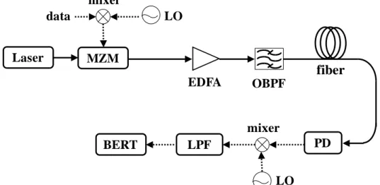
Combining the transmitter with communication channel and receiver, that is the model of ROF system, as shown in Fig. 2-5. We select the scheme of Fig. 2-3 (b) to become the transmitter in the model of ROF system.
Figure 2-5 The model of ROF system.
Laser MZM data mixer LO OBPF EDFA fiber PD LPF mixer LO BERT
12
2.5 The new proposed model of optical modulation system
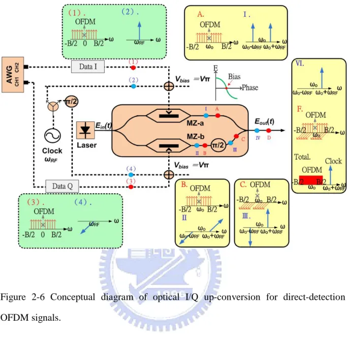
Figure 2-6 schematically depicts the principle of the proposed optical I/Q up-conversion for direct-detection OFDM signal generation. Data I and Q of OFDM signals are sent to MZ-a and MZ-b of the optical I/Q modulator, respectively. To achieve high optical modulation depth and to operate in E-field linear region of the MZM, both MZ-a and MZ-b are biased at the null point. Therefore, optical OFDM signal at the center frequency of optical carrier with carrier suppression is generated as shown in inset (D) of Fig. 2-6.
To realize direct-detection OFDM signals, we insert an optical subcarrier to induce remote beating by using SSB modulation with carrier suppression. Except with a phase difference of 90°, the RF signals sent into the MZ-a and MZ-b are exactly the same. Since both MZ-a and MZ-b are biased at the null point, the generated optical spectrum consists of an upper sideband (USB) and a lower sideband (LSB) with optical carrier suppression as shown in insets (I) and (II) of Fig. 2-6. When MZ-c is biased at the quadrature point, the polarity of LSB in inset (Ⅰ) opposes that in inset (Ⅲ). The LSB will be eliminated whereas the USB is obtained. Therefore, as both RF and OFDM signals are simultaneously sent to I/Q modulator, the generated optical DD-OFDM signal consisting of an un-modulated subcarrier and an OFDM-modulated carrier.
13
Figure 2-6 Conceptual diagram of optical I/Q up-conversion for direct-detection OFDM signals.
After square-law photo-diode (PD) detection, electrical RF-OFDM signals are obtained. Note that the proposed OFDM transmitter does not need an electrical mixer with a typical NF of more than 8 dB to avoid the beating noise interference, which is very important for highly spectral efficiency OFDM signals (i.e. 16-QAM or 64-QAM OFDM signal). Additionally, the relative intensity between the un-modulated and OFDM-modulated subcarriers can be easily tuned by adjusting the individual power of the electrical sinusoidal and OFDM signals to optimize the performance of the optical RF signals.
14
Chapter 3 The theoretical calculations of Proposed system 3.1 Introduce MZM
For MZM with configuration as Fig. 3-1, the output E-filed for upper arm is
EU = E0∙ a ∙ ej∆φ1 (1)
∆φ1 ≜vv1
π ∙ π (2)
∆φ1 is the optical carrier phase difference that is induced by v1, where a is the power
splitting ratio.
The output E-filed for upper arm is
EL = E0∙ √1 − a2∙ ej∆φ2 (3)
∆φ2 is the optical carrier phase difference that is induced by v2
∆φ2 ≜vv2π ∙ π (4)
The output E-filed for MZM is
ET = E0∙ �a ∙ b ∙ ej∆φ1 + √1 − a2∙ √1 − b2∙ ej∆φ2� (5)
where a and b are the power splitting ratios of the first and second Y-splitters in MZM, respectively. The power splitting ratio of two arms of a balanced MZM is 0.5. The electrical field at the output of the MZM is given by
ET =12∙ E0∙ {ej∆φ1 + ej∆φ2} (6)
ET = E0∙ cos �∆φ12−∆φ2� ∙ exp �j∆φ1+∆φ2 2� (7)
For single electro x-cut MZM. The electrical field at the output is given by EOUT = E0∙ cos �∆φ−(−∆φ)2 � ∙ exp �j∆φ+(−∆φ)2 � (8)
Add time component, the electrical field is
EOUT = E0∙ cos(∆φ) ∙ cos(𝜔𝜔0t) (9)
15
carrier, respectively; V(t) is the applied driving voltage, and ∆φ is the optical carrier phase difference that is induced by 𝑉𝑉(𝑡𝑡) between the two arms of the MZM. The loss of MZM is neglected. 𝑉𝑉(𝑡𝑡) consisting of an electrical sinusoidal signal and a dc biased voltage can be written as,
𝑉𝑉(𝑡𝑡) = 𝑉𝑉𝑏𝑏𝑏𝑏𝑏𝑏𝑏𝑏 + 𝑉𝑉𝑚𝑚 cos(𝜔𝜔t) (10)
where 𝑉𝑉𝑏𝑏𝑏𝑏𝑏𝑏𝑏𝑏 is the dc biased voltage, 𝑉𝑉𝑚𝑚 and 𝜔𝜔𝑅𝑅𝑅𝑅 are the amplitude and the angular frequency of the electrical driving signal, respectively. The optical carrier phase difference induced by 𝑉𝑉(𝑡𝑡) is given by
∆φ = 𝑉𝑉(𝑡𝑡)2V π = 𝑉𝑉𝑏𝑏𝑏𝑏𝑏𝑏𝑏𝑏+𝑉𝑉𝑚𝑚cos (𝜔𝜔t) Vπ ∙ π 2 (11)
Eq. (10) can be written as:
EOUT = E0∙ cos�Vbias +VVmcos(ωt)
π ∙
π
2� ∙ cos(ω0t) = E0∙ cos[b+ m ∙cos(ωRFt)] ∙ cos(ω0t)
= E0∙ cos(ω0t) ∙ {cos(b) ∙ cos[m ∙cos(ωRFt)]
−sin(b) ∙ sin[m ∙cos(ωRFt)]} (12)
where 𝑏𝑏 ≜𝑉𝑉𝑏𝑏𝑏𝑏𝑏𝑏𝑏𝑏
2Vπ π is a constant phase shift that is induced by the dc biased voltage,
and 𝑚𝑚 ≜ 𝑉𝑉𝑚𝑚
2Vππ is the phase modulation index.
⎩ ⎪ ⎨ ⎪
⎧cos(x sinθ) = J0(x) + 2 � J2n(x) cos(2nθ) ∞
n=1
sin(x sin θ) = 2 � J2n−1(x) sin[(2n − 1)θ] ∞ n=1 ⎩ ⎪ ⎨ ⎪
⎧cos(x cosθ) = J0(x) + 2 �(−1)nJ2n(x)cos(2nθ) ∞ n=1 sin(x cos θ) = 2 �(−1)nJ 2n−1(x)cos[(2n − 1)θ] ∞ n=1 (13)
16
Expanding Eq. (12) using Bessel functions, as detailed in Eq. (13). The electrical field at the output of the MZM can be written as:
EOUT = E0∙ cos(𝜔𝜔0𝑡𝑡) ∙ {cos(𝑏𝑏) ∙ [𝐽𝐽0(𝑚𝑚) + 2 ∙ �(−1)𝑛𝑛 ∙ 𝐽𝐽2𝑛𝑛(m) ∙ cos(2𝑛𝑛𝜔𝜔𝑅𝑅𝑅𝑅𝑡𝑡) ∞ i=1 ] −sin(𝑏𝑏) ∙ [2 ∙ �(−1)𝑛𝑛 ∙ 𝐽𝐽 2𝑛𝑛−1(𝑚𝑚) ∙ cos[(2𝑛𝑛 − 1)𝜔𝜔𝑅𝑅𝑅𝑅𝑡𝑡] ∞ i=1 ]} (14)
where 𝐽𝐽𝑛𝑛 is the Bessel function of the first kind of order n. the electrical field of the mm-wave signal can be written as
EOUT = E0∙ cos(𝑏𝑏) ∙ J0(m) ∙ cos(ω0t)
+E0∙ cos(𝑏𝑏) ∙ � 𝐽𝐽2𝑛𝑛(𝑚𝑚) ∙ cos[ ∞ i=1 (𝜔𝜔0− 2𝑛𝑛𝜔𝜔𝑅𝑅𝑅𝑅)𝑡𝑡 + 𝑛𝑛π] +E0∙ cos(𝑏𝑏) ∙ � 𝐽𝐽2𝑛𝑛(𝑚𝑚) ∙ cos[(𝜔𝜔0+ 2𝑛𝑛𝜔𝜔𝑅𝑅𝑅𝑅)𝑡𝑡 ∞ i=1 + 𝑛𝑛𝑛𝑛] −E0∙ sin(𝑏𝑏) ∙ � 𝐽𝐽2𝑛𝑛−1(𝑚𝑚) ∙ cos[
∞ i=1
𝜔𝜔0− (2𝑛𝑛 − 1)𝜔𝜔𝑅𝑅𝑅𝑅)𝑡𝑡 + 𝑛𝑛𝑛𝑛]
−E0∙ sin(𝑏𝑏) ∙ � 𝐽𝐽2𝑛𝑛−1(𝑚𝑚) ∙ cos[ ∞
i=1
𝜔𝜔0+ (2𝑛𝑛 − 1)𝜔𝜔𝑅𝑅𝑅𝑅)𝑡𝑡 + 𝑛𝑛𝑛𝑛]
17
3.2 Theoretical calculation of single drive MZM 3.2.1 Bias at maximum transmission point
When the MZM is biased at the maximum transmission point, the bias voltage is set at 𝑉𝑉𝑏𝑏𝑏𝑏𝑏𝑏𝑏𝑏 = 0, and cos 𝑏𝑏 = 1 and sin 𝑏𝑏 = 0. Consequently, the electrical field of the mm-wave signal can be written as
𝐸𝐸𝑂𝑂𝑂𝑂𝑂𝑂(𝑡𝑡) = 𝐸𝐸0∙ 𝐽𝐽0(𝑚𝑚) ∙ cos(𝜔𝜔0𝑡𝑡) +𝐸𝐸0∙ � 𝐽𝐽2𝑛𝑛(𝑚𝑚) ∙ cos[ ∞ 𝑛𝑛=1 (𝜔𝜔0− 2𝑛𝑛𝜔𝜔𝑅𝑅𝑅𝑅)𝑡𝑡 + 𝑛𝑛𝑛𝑛] +𝐸𝐸0∙ � 𝐽𝐽2𝑛𝑛(𝑚𝑚) ∙ cos[(𝜔𝜔0 + 2𝑛𝑛𝜔𝜔𝑅𝑅𝑅𝑅)𝑡𝑡 ∞ 𝑛𝑛=1 + 𝑛𝑛𝑛𝑛] (16)
The amplitudes of the generated optical sidebands are proportional to those of the corresponding Bessel functions associated with the phase modulation index 𝑚𝑚. With the amplitude of the electrical driving signal 𝑉𝑉𝑚𝑚 equal to 𝑉𝑉𝑛𝑛, the maximum 𝑚𝑚 is 𝑛𝑛
2.
18 As 0 < 𝑚𝑚 <𝑛𝑛
2, the Bessel function 𝐽𝐽𝑛𝑛 for 𝑛𝑛 ≥ 1 decreases and increases with the
order of Bessel function and m, respectively, as shown in Figure 3-2. 𝐽𝐽1�𝑛𝑛
2�, 𝐽𝐽2� 𝑛𝑛 2�,
𝐽𝐽3�𝑛𝑛2�, and 𝐽𝐽4�𝑛𝑛2� are 0.5668, 0.2497, 0.069, and 0.014, respectively. Therefore, the
optical sidebands with the Bessel function higher than 𝐽𝐽3(𝔪𝔪) can be ignored, and Eq. (14) can be further simplified to
𝐸𝐸𝑂𝑂𝑂𝑂𝑂𝑂 = 𝐸𝐸0∙ 𝐽𝐽0(𝑚𝑚) ∙ cos(𝜔𝜔0𝑡𝑡) +𝐸𝐸0∙ 𝐽𝐽2(𝑚𝑚) ∙ cos[(𝜔𝜔0− 2𝜔𝜔𝑅𝑅𝑅𝑅)𝑡𝑡 + 𝑛𝑛] +𝐸𝐸0∙ 𝐽𝐽2(𝑚𝑚) ∙ cos[(𝜔𝜔0+ 2𝜔𝜔𝑅𝑅𝑅𝑅)𝑡𝑡 + 𝑛𝑛] +𝐸𝐸0∙ 𝐽𝐽4(𝑚𝑚) ∙ cos[(𝜔𝜔0− 4𝜔𝜔𝑅𝑅𝑅𝑅)𝑡𝑡] +𝐸𝐸0∙ 𝐽𝐽4(𝑚𝑚) ∙ cos[(𝜔𝜔0+ 4𝜔𝜔𝑅𝑅𝑅𝑅)𝑡𝑡] (17) 0 2 4 6 8 10 -0.5 0.0 0.5 1.0
m
J0
J1
J2
J3
19 3.2.2 Bias at quadrature point
When the MZM is biased at the quadrature point, the bias voltage is set at 𝑉𝑉𝑏𝑏𝑏𝑏𝑏𝑏𝑏𝑏 =V2π, and cos 𝑏𝑏 = √22 and sin 𝑏𝑏 =√22. Consequently, the electrical field of the
mm-wave signal can be written as
EOUT = 1 √2∙ E0∙ J0(m) ∙ cos(ω0t) + 1 √2∙ E0∙ J1(m) ∙ cos[(ω0− ωRF)t] + 1 √2∙ E0∙ J1(m) ∙ cos[(ω0+ ωRF)t] + 1 √2∙ E0∙ J2(m) ∙ cos[(ω0− 2ωRF)t + π] + 1 √2∙ E0∙ J2(m) ∙ cos[(ω0+ 2ωRF)t + π] + 1 √2∙ E0∙ J3(m) ∙ cos[(ω0− 3ωRF)t + π] + 1 √2∙ E0∙ J3(m) ∙ cos[(ω0+ 3ωRF)t + π] (18) 3.2.3 Bias at null point
When the MZM is biased at the null point, the bias voltage is set at 𝑉𝑉𝑏𝑏𝑏𝑏𝑏𝑏𝑏𝑏 = Vπ,
and cos 𝑏𝑏 = 0 and sin 𝑏𝑏 = 1. Consequently, the electrical field of the mm-wave
signal using DSBCS modulation can be written as EOUT = E0∙ J1(m) ∙ cos[(ω0− ωRF)t] +E0∙ J1(m) ∙ cos[(ω0+ ωRF)t] +E0∙ J3(m) ∙ cos[(ω0− 3ωRF)t + π] +E0∙ J3(m) ∙ cos[(ω0+ 3ωRF)t + π] +E0∙ J5(m) ∙ cos[(ω0− 5ωRF)t] +E0∙ J5(m) ∙ cos[(ω0+ 5ωRF)t]
20 3.3 Theoretical calculations
3.3.1 The generated optical signal
The theoretical calculations of proposed system, the driving RF signal 𝑉𝑉(𝑡𝑡)𝑢𝑢𝑢𝑢 and 𝑉𝑉(𝑡𝑡)𝑑𝑑𝑑𝑑𝑑𝑑𝑛𝑛 consisting of an electrical sinusoidal signal and a dc biased voltage can be
written as
𝑉𝑉(𝑡𝑡)𝑢𝑢𝑢𝑢 = 𝑉𝑉𝑏𝑏𝑏𝑏𝑏𝑏𝑏𝑏 + 𝑉𝑉1cos𝜔𝜔1t + 𝑉𝑉2cos𝜔𝜔2t
𝑉𝑉(𝑡𝑡)𝑑𝑑𝑑𝑑𝑑𝑑𝑛𝑛 = 𝑉𝑉𝑏𝑏𝑏𝑏𝑏𝑏𝑏𝑏 + 𝑉𝑉1cos𝜔𝜔1t + 𝑉𝑉2cos𝜔𝜔2t (20)
where 𝑉𝑉𝑏𝑏𝑏𝑏𝑏𝑏𝑏𝑏 is the dc biased voltage, 𝑉𝑉1, 𝑉𝑉2 and 𝜔𝜔1, 𝜔𝜔2 are the amplitude and the angular frequency of the electrical driving signals, respectively. The optical carrier phase difference induced by 𝑉𝑉(𝑡𝑡) is given by
𝐸𝐸𝑂𝑂𝑂𝑂𝑂𝑂_𝑢𝑢𝑢𝑢 = 𝐸𝐸0∙ cos[2Vππ(𝑉𝑉𝑏𝑏𝑏𝑏𝑏𝑏𝑏𝑏 + 𝑉𝑉1cos𝜔𝜔1t + 𝑉𝑉2cos𝜔𝜔2t)]
𝐸𝐸𝑂𝑂𝑂𝑂𝑂𝑂_𝑑𝑑𝑑𝑑𝑑𝑑𝑛𝑛 = 𝐸𝐸0∙ cos[2Vπ
π(𝑉𝑉𝑏𝑏𝑏𝑏𝑏𝑏𝑏𝑏 + 𝑉𝑉1cos𝜔𝜔1t + 𝑉𝑉2cos𝜔𝜔2t)]
𝐸𝐸𝑂𝑂𝑂𝑂𝑂𝑂_𝑢𝑢𝑢𝑢 = 𝐸𝐸0∙ cos[𝑏𝑏 + 𝑚𝑚1cos𝜔𝜔1t + 𝑚𝑚2cos𝜔𝜔2t]
𝐸𝐸𝑂𝑂𝑂𝑂𝑂𝑂_𝑑𝑑𝑑𝑑𝑑𝑑𝑛𝑛 = 𝐸𝐸0∙ cos[𝑏𝑏 + 𝑚𝑚1cos(𝜔𝜔1t +π2) + 𝑚𝑚2cos𝜔𝜔2t] (21)
where 𝑏𝑏 ≜𝑉𝑉𝑏𝑏𝑏𝑏𝑏𝑏𝑏𝑏π
2π is a constant phase shift that is induced by the dc biased voltage, and
𝑚𝑚1 =2V𝑉𝑉1ππ,𝑚𝑚2 =2V𝑉𝑉2ππ is the phase modulation index.
𝐸𝐸𝑂𝑂𝑂𝑂𝑂𝑂_𝑢𝑢𝑢𝑢 = 𝐸𝐸0∙ cos𝑏𝑏 ∙ cos(𝑚𝑚1cos𝜔𝜔1t + 𝑚𝑚2cos𝜔𝜔2t)
−𝐸𝐸0∙ sin𝑏𝑏 ∙ sin(𝑚𝑚1cos𝜔𝜔1t + 𝑚𝑚2cos𝜔𝜔2t)
𝐸𝐸𝑂𝑂𝑂𝑂𝑂𝑂_𝑑𝑑𝑑𝑑𝑑𝑑𝑛𝑛 = 𝐸𝐸0∙ cos𝑏𝑏 ∙ cos(𝑚𝑚1cos(𝜔𝜔1t + π/2) + 𝑚𝑚2cos𝜔𝜔2t)
21
𝐸𝐸𝑂𝑂𝑂𝑂𝑂𝑂_𝑢𝑢𝑢𝑢 = 𝐸𝐸0∙ cos𝑏𝑏{cos(m1cos𝜔𝜔1𝑡𝑡)cos(𝑚𝑚2cos𝜔𝜔2𝑡𝑡)
−sin(𝑚𝑚1cos𝜔𝜔1𝑡𝑡)sin(𝑚𝑚2cos𝜔𝜔2𝑡𝑡)}
−𝐸𝐸0∙ sin𝑏𝑏{sin(𝑚𝑚1cos𝜔𝜔1t)cos(𝑚𝑚2cos𝜔𝜔2t)
+cos(𝑚𝑚1cos𝜔𝜔1t)sin(𝑚𝑚2cos𝜔𝜔2t)}
𝐸𝐸𝑂𝑂𝑂𝑂𝑂𝑂_𝑑𝑑𝑑𝑑𝑑𝑑𝑛𝑛 = 𝐸𝐸0∙ cos𝑏𝑏{cos(m1cos(𝜔𝜔1t + π/2))cos(𝑚𝑚2cos𝜔𝜔2𝑡𝑡)
−sin(𝑚𝑚1cos(𝜔𝜔1t + π/2))sin(𝑚𝑚2cos𝜔𝜔2𝑡𝑡)}
−𝐸𝐸0∙ sin𝑏𝑏{sin(𝑚𝑚1cos(𝜔𝜔1t + π/2))cos(𝑚𝑚2cos𝜔𝜔2t)
+cos(𝑚𝑚1cos(𝜔𝜔1t + π/2))sin(𝑚𝑚2cos𝜔𝜔2t)} (22)
When the MZM is biased at the null point, the bias voltage is set at 𝑉𝑉𝑏𝑏𝑏𝑏𝑏𝑏𝑏𝑏 = Vπ, and cos 𝑏𝑏 = 0 and sin 𝑏𝑏 = 1. Consequently, the electrical field of the mm-wave signal using SSBCS modulation can be written as
𝐸𝐸𝑂𝑂𝑂𝑂𝑂𝑂_𝑢𝑢𝑢𝑢 = −𝐸𝐸0{sin(𝑚𝑚1cos𝜔𝜔1t)cos(𝑚𝑚2cos𝜔𝜔2t)
+cos(𝑚𝑚1cos𝜔𝜔1t)sin(𝑚𝑚2cos𝜔𝜔2t)}
𝐸𝐸𝑂𝑂𝑂𝑂𝑂𝑂_𝑑𝑑𝑑𝑑𝑑𝑑𝑛𝑛 = −𝐸𝐸0{sin(𝑚𝑚1cos(𝜔𝜔1t + π/2))cos(𝑚𝑚2cos𝜔𝜔2t)
+cos(𝑚𝑚1cos(𝜔𝜔1t + π/2))sin(𝑚𝑚2cos𝜔𝜔2t)} (23)
First, to expand equation sin(𝑚𝑚1cos𝜔𝜔1t)cos(𝑚𝑚2cos𝜔𝜔2t) sin(𝑚𝑚1cos𝜔𝜔1t)cos(𝑚𝑚2cos𝜔𝜔2t)
= �2 �(−1)nJ 2n−1(𝑚𝑚1)cos[(2n − 1)𝜔𝜔1t] ∞ n=1 � ∙ �J0(𝑚𝑚2) + 2 �(−1)nJ2n(𝑚𝑚2)cos(2n𝜔𝜔2t) ∞ n=1 � = {−2J1(𝑚𝑚1)cos(𝜔𝜔1t) + 2J3(𝑚𝑚1)cos(3𝜔𝜔1t) − ⋯ } ∙ {J0(𝑚𝑚2) − 2J2(𝑚𝑚2)cos(2𝜔𝜔2t)+2J4(𝑚𝑚2)cos(4𝜔𝜔2t) − ⋯ }
22 = �2 �(−1)nJ 2n−1(𝑚𝑚1)cos[(2n − 1)𝜔𝜔1t + (2n − 1)π/2] ∞ n=1 � ∙ �J0(𝑚𝑚2) + 2 �(−1)nJ2n(𝑚𝑚2)cos(2n𝜔𝜔2t) ∞ n=1 � = {−2J1(𝑚𝑚1)cos(𝜔𝜔1t + π/2) + 2J3(𝑚𝑚1)cos(3𝜔𝜔1t + 3π/2) − ⋯ } ∙ {J0(𝑚𝑚2) − 2J2(𝑚𝑚2)cos(2𝜔𝜔2t)+2J4(𝑚𝑚2)cos(4𝜔𝜔2t) − ⋯ } (24)
The optical sidebands with the Bessel function higher than 𝐽𝐽3(𝔪𝔪) can be ignored. Consequently, the electrical field can be written as
sin(𝑚𝑚1cos𝜔𝜔1t)cos(𝑚𝑚2cos𝜔𝜔2t)
≈ −2J0(𝑚𝑚2)J1(𝑚𝑚1)cos𝜔𝜔1t
+2J0(𝑚𝑚2)J3(𝑚𝑚1)cos(3𝜔𝜔1t)
+4J1(𝑚𝑚1)J2(𝑚𝑚2) ∙21[cos(𝜔𝜔1+ 2𝜔𝜔2) t + cos(𝜔𝜔1− 2𝜔𝜔2) t]
−4J2(𝑚𝑚2)J3(𝑚𝑚1) ∙21[cos(3𝜔𝜔1+ 2𝜔𝜔2) t + cos(3𝜔𝜔1− 2𝜔𝜔2) t]
sin(𝑚𝑚1cos(𝜔𝜔1t + π/2))cos(𝑚𝑚2cos𝜔𝜔2t)
≈ −2J0(𝑚𝑚2)J1(𝑚𝑚1)cos(𝜔𝜔1t + π/2)
+2J0(𝑚𝑚2)J3(𝑚𝑚1)cos(3𝜔𝜔1t + 3π/2)
+4J1(𝑚𝑚1)J2(𝑚𝑚2) ∙21[cos((𝜔𝜔1+ 2𝜔𝜔2) t + 𝑛𝑛/2) + cos((𝜔𝜔1− 2𝜔𝜔2) t + 𝑛𝑛/2)]
−4J2(𝑚𝑚2)J3(𝑚𝑚1) ∙21[cos((3𝜔𝜔1+ 2𝜔𝜔2) t + 3𝑛𝑛/2) + cos((3𝜔𝜔1− 2𝜔𝜔2) t + 3𝑛𝑛/2)]
23 Add time component cos(𝜔𝜔𝑐𝑐t)
sin(𝑚𝑚1cos𝜔𝜔1t)cos(𝑚𝑚2cos𝜔𝜔2t)cos(𝜔𝜔𝑐𝑐t)
= −2J0(𝑚𝑚2)J1(𝑚𝑚1)cos𝜔𝜔1t cos(𝜔𝜔𝑐𝑐t)
+2J0(𝑚𝑚2)J3(𝑚𝑚1)cos(3𝜔𝜔1t)cos(𝜔𝜔𝑐𝑐t)
+4J1(𝑚𝑚1)J2(𝑚𝑚2) ∙12[cos(𝜔𝜔1+ 2𝜔𝜔2) t + cos(𝜔𝜔1− 2𝜔𝜔2) t]cos(𝜔𝜔𝑐𝑐t)
−4J2(𝑚𝑚2)J3(𝑚𝑚1) ∙12[cos(3𝜔𝜔1+ 2𝜔𝜔2) t + cos(3𝜔𝜔1− 2𝜔𝜔2) t]cos(𝜔𝜔𝑐𝑐t)
sin(𝑚𝑚1cos(𝜔𝜔1t + π/2))cos(𝑚𝑚2cos𝜔𝜔2t)cos(𝜔𝜔𝑐𝑐t + π/2)
= −2J0(𝑚𝑚2)J1(𝑚𝑚1)cos(𝜔𝜔1t + π/2) cos(𝜔𝜔𝑐𝑐t + π/2)
+2J0(𝑚𝑚2)J3(𝑚𝑚1)cos(3𝜔𝜔1t + 3π/2)cos(𝜔𝜔𝑐𝑐t + π/2)
+4J1(𝑚𝑚1)J2(𝑚𝑚2) ∙12[cos(𝜔𝜔1+ π/2 + 2𝜔𝜔2) t + cos(𝜔𝜔1+ π/2 − 2𝜔𝜔2) t]cos(𝜔𝜔𝑐𝑐t
+ π/2) −4J2(𝑚𝑚2)J3(𝑚𝑚1)
∙1
2[cos(3𝜔𝜔1+ 3π/2 + 2𝜔𝜔2) t + cos(3𝜔𝜔1+ 3π/2 − 2𝜔𝜔2) t]cos(𝜔𝜔𝑐𝑐t + π/2)
(26)
J0(𝑚𝑚2)J1(𝑚𝑚1), 2J0(𝑚𝑚2)J3(𝑚𝑚1), 4J1(𝑚𝑚1)J2(𝑚𝑚2), and 4J2(𝑚𝑚2)J3(𝑚𝑚1) are shown in
Figure 3-3. Therefore, the optical sidebands with the Bessel function 4J2(𝑚𝑚2)J3(𝑚𝑚1) can be ignored, and Eq. (14) can be further simplified to
24 sin(𝑚𝑚1cos𝜔𝜔1t)cos(𝑚𝑚2cos𝜔𝜔2t)cos(𝜔𝜔𝑐𝑐t)
= −J0(𝑚𝑚2)J1(𝑚𝑚1)[cos(𝜔𝜔𝑐𝑐 + 𝜔𝜔1)t + cos(𝜔𝜔𝑐𝑐 − 𝜔𝜔1)t]
+J0(𝑚𝑚2)J3(𝑚𝑚1)[cos(𝜔𝜔𝑐𝑐 + 3𝜔𝜔1)t + cos(𝜔𝜔𝑐𝑐 − 3𝜔𝜔1)t]
+J1(𝑚𝑚1)J2(𝑚𝑚2)[cos(𝜔𝜔𝑐𝑐 + 𝜔𝜔1+ 2𝜔𝜔2) t + cos(𝜔𝜔𝑐𝑐 − 𝜔𝜔1− 2𝜔𝜔2) t]
+J1(𝑚𝑚1)J2(𝑚𝑚2)[cos(𝜔𝜔𝑐𝑐 + 𝜔𝜔1− 2𝜔𝜔2) t + cos(𝜔𝜔𝑐𝑐 − 𝜔𝜔1+ 2𝜔𝜔2) t]
sin(𝑚𝑚1cos𝜔𝜔1t + π/2)cos(𝑚𝑚2cos𝜔𝜔2t)cos(𝜔𝜔𝑐𝑐t + π/2)
= −J0(𝑚𝑚2)J1(𝑚𝑚1)[cos(𝜔𝜔𝑐𝑐 + 𝜔𝜔1+ π)t + cos(𝜔𝜔𝑐𝑐 − 𝜔𝜔1)t]
+J0(𝑚𝑚2)J3(𝑚𝑚1)[cos(𝜔𝜔𝑐𝑐 + 3𝜔𝜔1+ 2π)t + cos(𝜔𝜔𝑐𝑐 − 3𝜔𝜔1− π)t]
+J1(𝑚𝑚1)J2(𝑚𝑚2)[cos(𝜔𝜔𝑐𝑐 + 𝜔𝜔1+ 2𝜔𝜔2+ π) t + cos(𝜔𝜔𝑐𝑐 − 𝜔𝜔1− 2𝜔𝜔2) t]
+J1(𝑚𝑚1)J2(𝑚𝑚2)[cos(𝜔𝜔𝑐𝑐 + 𝜔𝜔1− 2𝜔𝜔2+ π) t + cos(𝜔𝜔𝑐𝑐 − 𝜔𝜔1+ 2𝜔𝜔2) t]
(27)
Second: To expand equation cos(𝑚𝑚1cos𝜔𝜔1t)sin(𝑚𝑚2cos𝜔𝜔2t) and cos(𝑚𝑚1cos(𝜔𝜔1t +
π
2))sin(𝑚𝑚2cos𝜔𝜔2t)
cos(𝑚𝑚1cos𝜔𝜔1𝑡𝑡)sin(𝑚𝑚2cos𝜔𝜔2𝑡𝑡)
= �𝐽𝐽0(𝑚𝑚1) + 2 �(−1)𝑛𝑛𝐽𝐽2𝑛𝑛(𝑚𝑚1)cos(2𝑛𝑛𝜔𝜔1𝑡𝑡) ∞ 𝑛𝑛=1 � ∙ �2 �(−1)𝑛𝑛𝐽𝐽 2𝑛𝑛−1(𝑚𝑚2)cos[(2𝑛𝑛 − 1)𝜔𝜔2𝑡𝑡] ∞ 𝑛𝑛=1 � = {𝐽𝐽0(𝑚𝑚1) − 2𝐽𝐽2(𝑚𝑚1)cos(2𝜔𝜔1𝑡𝑡)+2𝐽𝐽4(𝑚𝑚1)cos(4𝜔𝜔1𝑡𝑡) − ⋯ } ∙ {−2𝐽𝐽1(𝑚𝑚2)cos(𝜔𝜔2𝑡𝑡) + 2𝐽𝐽3(𝑚𝑚2)cos(3𝜔𝜔2𝑡𝑡) − ⋯ } ≈ −2𝐽𝐽0(𝑚𝑚1)𝐽𝐽1(𝑚𝑚2)cos𝜔𝜔2𝑡𝑡 +2𝐽𝐽0(𝑚𝑚1)𝐽𝐽3(𝑚𝑚2)cos(3𝜔𝜔2𝑡𝑡) +4𝐽𝐽1(𝑚𝑚2)𝐽𝐽2(𝑚𝑚1) ∙21[cos(𝜔𝜔2+ 2𝜔𝜔1) 𝑡𝑡 + cos(𝜔𝜔2− 2𝜔𝜔1) 𝑡𝑡]
25
−4𝐽𝐽2(𝑚𝑚1)𝐽𝐽3(𝑚𝑚2) ∙21[cos(3𝜔𝜔2+ 2𝜔𝜔1) 𝑡𝑡 + cos(3𝜔𝜔2− 2𝜔𝜔1) 𝑡𝑡]
cos(𝑚𝑚1cos(𝜔𝜔1t +π2))sin(𝑚𝑚2cos𝜔𝜔2t)
≈ −2𝐽𝐽0(𝑚𝑚1)𝐽𝐽1(𝑚𝑚2)cos𝜔𝜔2𝑡𝑡
+2𝐽𝐽0(𝑚𝑚1)𝐽𝐽3(𝑚𝑚2)cos(3𝜔𝜔2𝑡𝑡)
+4𝐽𝐽1(𝑚𝑚2)𝐽𝐽2(𝑚𝑚1) ∙21[cos(𝜔𝜔2+ 2𝜔𝜔1+ 𝑛𝑛) 𝑡𝑡 + cos(𝜔𝜔2− 2𝜔𝜔1− 𝑛𝑛) 𝑡𝑡]
−4𝐽𝐽2(𝑚𝑚1)𝐽𝐽3(𝑚𝑚2) ∙21[cos(3𝜔𝜔2+ 2𝜔𝜔1+ 𝑛𝑛) 𝑡𝑡 + cos(3𝜔𝜔2− 2𝜔𝜔1− 𝑛𝑛) 𝑡𝑡]
(28) Add time component cos(𝜔𝜔𝑐𝑐𝑡𝑡)
cos(𝑚𝑚1cos𝜔𝜔1𝑡𝑡)sin(𝑚𝑚2cos𝜔𝜔2𝑡𝑡)cos(𝜔𝜔𝑐𝑐𝑡𝑡)
= −2𝐽𝐽0(𝑚𝑚1)𝐽𝐽1(𝑚𝑚2)cos𝜔𝜔2𝑡𝑡 cos(𝜔𝜔𝑐𝑐𝑡𝑡)
+2𝐽𝐽0(𝑚𝑚1)𝐽𝐽3(𝑚𝑚2)cos(3𝜔𝜔2𝑡𝑡) cos(𝜔𝜔𝑐𝑐𝑡𝑡)
+4𝐽𝐽1(𝑚𝑚2)𝐽𝐽2(𝑚𝑚1) ∙12[cos(𝜔𝜔2+ 2𝜔𝜔1) 𝑡𝑡 + cos(𝜔𝜔2− 2𝜔𝜔1) 𝑡𝑡]cos(𝜔𝜔𝑐𝑐𝑡𝑡)
−4𝐽𝐽2(𝑚𝑚1)𝐽𝐽3(𝑚𝑚2) ∙12[cos(3𝜔𝜔2+ 2𝜔𝜔1) 𝑡𝑡 + cos(3𝜔𝜔2− 2𝜔𝜔1) 𝑡𝑡]cos(𝜔𝜔𝑐𝑐𝑡𝑡)
= −𝐽𝐽0(𝑚𝑚1)𝐽𝐽1(𝑚𝑚2)[cos(𝜔𝜔𝑐𝑐 + 𝜔𝜔2)𝑡𝑡 + cos(𝜔𝜔𝑐𝑐 − 𝜔𝜔2)𝑡𝑡]
+𝐽𝐽0(𝑚𝑚1)𝐽𝐽3(𝑚𝑚2)[cos(𝜔𝜔𝑐𝑐 + 3𝜔𝜔2)𝑡𝑡 + cos(𝜔𝜔𝑐𝑐 − 3𝜔𝜔2)𝑡𝑡]
+𝐽𝐽1(𝑚𝑚2)𝐽𝐽2(𝑚𝑚1)[cos(𝜔𝜔𝑐𝑐 + 𝜔𝜔2+ 2𝜔𝜔1) 𝑡𝑡 + cos((𝜔𝜔𝑐𝑐 − 𝜔𝜔2− 2𝜔𝜔1) 𝑡𝑡]
+𝐽𝐽1(𝑚𝑚2)𝐽𝐽2(𝑚𝑚1)[cos(𝜔𝜔𝑐𝑐 + 𝜔𝜔2− 2𝜔𝜔1) 𝑡𝑡 + cos(𝜔𝜔𝑐𝑐 − 𝜔𝜔2+ 2𝜔𝜔1) 𝑡𝑡]
cos(𝑚𝑚1cos(𝜔𝜔1𝑡𝑡 + 𝑛𝑛/2)sin(𝑚𝑚2cos𝜔𝜔2𝑡𝑡)cos(𝜔𝜔𝑐𝑐𝑡𝑡+π/2)
= −𝐽𝐽0(𝑚𝑚1)𝐽𝐽1(𝑚𝑚2)[cos((𝜔𝜔𝑐𝑐 + 𝜔𝜔2)𝑡𝑡 + π/2) + cos((𝜔𝜔𝑐𝑐 − 𝜔𝜔2)𝑡𝑡 + π/2)]
26
+𝐽𝐽1(𝑚𝑚2)𝐽𝐽2(𝑚𝑚1)[cos((𝜔𝜔𝑐𝑐 + 𝜔𝜔2+ 2𝜔𝜔1) 𝑡𝑡 + 3π/2) + cos((𝜔𝜔𝑐𝑐 − 𝜔𝜔2− 2𝜔𝜔1) 𝑡𝑡
− π/2)]
+𝐽𝐽1(𝑚𝑚2)𝐽𝐽2(𝑚𝑚1)[cos((𝜔𝜔𝑐𝑐 + 𝜔𝜔2− 2𝜔𝜔1) 𝑡𝑡 − π/2) + cos((𝜔𝜔𝑐𝑐 − 𝜔𝜔2+ 2𝜔𝜔1) 𝑡𝑡 +
3π/2) (29)
The output electrical filed can be rewritten as
𝐸𝐸𝑂𝑂𝑂𝑂𝑂𝑂𝑢𝑢𝑢𝑢(𝑡𝑡) = 𝐸𝐸0cos(𝜔𝜔𝑐𝑐𝑡𝑡) {sin(𝑚𝑚1cos𝜔𝜔1𝑡𝑡)cos(𝑚𝑚2cos𝜔𝜔2𝑡𝑡)
+cos(𝑚𝑚1cos𝜔𝜔1𝑡𝑡)sin(𝑚𝑚2cos𝜔𝜔2𝑡𝑡)}
𝐸𝐸𝑂𝑂𝑂𝑂𝑂𝑂_𝑑𝑑𝑑𝑑𝑑𝑑𝑛𝑛 = −𝐸𝐸0cos(𝜔𝜔𝑐𝑐𝑡𝑡 + 𝑛𝑛/2){sin(𝑚𝑚1cos(𝜔𝜔1t + π/2))cos(𝑚𝑚2cos𝜔𝜔2t)
+cos(𝑚𝑚1cos(𝜔𝜔1t + π/2))sin(𝑚𝑚2cos𝜔𝜔2t)}
𝐸𝐸𝑂𝑂𝑂𝑂𝑂𝑂_𝑢𝑢𝑢𝑢(t) = 𝐸𝐸0∙ {𝐽𝐽0(𝑚𝑚2)𝐽𝐽1(𝑚𝑚1)[cos(𝜔𝜔𝑐𝑐 + 𝜔𝜔1)𝑡𝑡 + cos(𝜔𝜔𝑐𝑐 − 𝜔𝜔1)𝑡𝑡] −𝐽𝐽0(𝑚𝑚2)𝐽𝐽3(𝑚𝑚1)[cos(𝜔𝜔𝑐𝑐 + 3𝜔𝜔1)𝑡𝑡 + cos(𝜔𝜔𝑐𝑐 − 3𝜔𝜔1)𝑡𝑡] −𝐽𝐽1(𝑚𝑚1)𝐽𝐽2(𝑚𝑚2)[cos(𝜔𝜔𝑐𝑐 + 𝜔𝜔1+ 2𝜔𝜔2) 𝑡𝑡 + cos(𝜔𝜔𝑐𝑐 − 𝜔𝜔1− 2𝜔𝜔2) 𝑡𝑡] −𝐽𝐽1(𝑚𝑚1)𝐽𝐽2(𝑚𝑚2)[cos(𝜔𝜔𝑐𝑐 + 𝜔𝜔1− 2𝜔𝜔2) 𝑡𝑡 + cos(𝜔𝜔𝑐𝑐 − 𝜔𝜔1+ 2𝜔𝜔2) 𝑡𝑡] +𝐽𝐽0(𝑚𝑚1)𝐽𝐽1(𝑚𝑚2)[cos(𝜔𝜔𝑐𝑐 + 𝜔𝜔2)𝑡𝑡 + cos(𝜔𝜔𝑐𝑐 − 𝜔𝜔2)𝑡𝑡] −𝐽𝐽0(𝑚𝑚1)𝐽𝐽3(𝑚𝑚2)[cos(𝜔𝜔𝑐𝑐 + 3𝜔𝜔2)𝑡𝑡 + cos(𝜔𝜔𝑐𝑐 − 3𝜔𝜔2)𝑡𝑡] −𝐽𝐽1(𝑚𝑚2)𝐽𝐽2(𝑚𝑚1)[cos(𝜔𝜔𝑐𝑐 + 𝜔𝜔2+ 2𝜔𝜔1) 𝑡𝑡 + cos(𝜔𝜔𝑐𝑐 − 𝜔𝜔2− 2𝜔𝜔1) 𝑡𝑡] −𝐽𝐽1(𝑚𝑚2)𝐽𝐽2(𝑚𝑚1)[cos(𝜔𝜔𝑐𝑐 + 𝜔𝜔2− 2𝜔𝜔1) 𝑡𝑡 + cos(𝜔𝜔𝑐𝑐 − 𝜔𝜔2+ 2𝜔𝜔1) 𝑡𝑡]} 𝐸𝐸𝑂𝑂𝑂𝑂𝑂𝑂𝑑𝑑𝑑𝑑𝑑𝑑𝑛𝑛 (t) = 𝐸𝐸0∙ {𝐽𝐽0(𝑚𝑚2)𝐽𝐽1(𝑚𝑚1)[cos((𝜔𝜔𝑐𝑐 + 𝜔𝜔1)𝑡𝑡 + 𝑛𝑛) + cos((𝜔𝜔𝑐𝑐 − 𝜔𝜔1)𝑡𝑡)] −𝐽𝐽0(𝑚𝑚2)𝐽𝐽3(𝑚𝑚1)[cos((𝜔𝜔𝑐𝑐 + 3𝜔𝜔1)𝑡𝑡 + 2𝑛𝑛) + cos((𝜔𝜔𝑐𝑐 − 3𝜔𝜔1)𝑡𝑡 − 2𝑛𝑛)] −𝐽𝐽1(𝑚𝑚1)𝐽𝐽2(𝑚𝑚2)[cos((𝜔𝜔𝑐𝑐 + 𝜔𝜔1+ 2𝜔𝜔2) 𝑡𝑡 + 𝑛𝑛) + cos((𝜔𝜔𝑐𝑐 − 𝜔𝜔1− 2𝜔𝜔2) 𝑡𝑡)] −𝐽𝐽1(𝑚𝑚1)𝐽𝐽2(𝑚𝑚2)[cos((𝜔𝜔𝑐𝑐 + 𝜔𝜔1− 2𝜔𝜔2) 𝑡𝑡 + 𝑛𝑛) + cos((𝜔𝜔𝑐𝑐 − 𝜔𝜔1+ 2𝜔𝜔2) 𝑡𝑡)]
27 +𝐽𝐽0(𝑚𝑚1)𝐽𝐽1(𝑚𝑚2)[cos((𝜔𝜔𝑐𝑐 + 𝜔𝜔2)𝑡𝑡 +𝑛𝑛2) + cos((𝜔𝜔𝑐𝑐 − 𝜔𝜔2)𝑡𝑡 +𝑛𝑛2)] −𝐽𝐽0(𝑚𝑚1)𝐽𝐽3(𝑚𝑚2)[cos((𝜔𝜔𝑐𝑐 + 3𝜔𝜔2)𝑡𝑡 +𝑛𝑛2) + cos((𝜔𝜔𝑐𝑐 − 3𝜔𝜔2)𝑡𝑡 +𝑛𝑛2)] −𝐽𝐽1(𝑚𝑚2)𝐽𝐽2(𝑚𝑚1) �cos((𝜔𝜔𝑐𝑐 + 𝜔𝜔2+ 2𝜔𝜔1) 𝑡𝑡 +3𝑛𝑛2 ) + cos((𝜔𝜔𝑐𝑐 − 𝜔𝜔2− 2𝜔𝜔1) 𝑡𝑡 −𝑛𝑛2)� −𝐽𝐽1(𝑚𝑚2)𝐽𝐽2(𝑚𝑚1) �cos((𝜔𝜔𝑐𝑐 + 𝜔𝜔2− 2𝜔𝜔1) 𝑡𝑡 −𝑛𝑛2) + cos((𝜔𝜔𝑐𝑐 − 𝜔𝜔2+ 2𝜔𝜔1) 𝑡𝑡 +3𝑛𝑛2 )�} (30) 𝐸𝐸𝑂𝑂𝑂𝑂𝑂𝑂(t) = 𝐸𝐸𝑂𝑂𝑂𝑂𝑂𝑂𝑢𝑢𝑢𝑢(t) + 𝐸𝐸𝑂𝑂𝑂𝑂𝑂𝑂𝑑𝑑𝑑𝑑𝑑𝑑𝑛𝑛 (t) = 𝐸𝐸0∙ 2{𝐽𝐽0(𝑚𝑚2)𝐽𝐽1(𝑚𝑚1)cos(𝜔𝜔𝑐𝑐 − 𝜔𝜔1)𝑡𝑡] −2𝐽𝐽0(𝑚𝑚2)𝐽𝐽3(𝑚𝑚1)[cos(𝜔𝜔𝑐𝑐 + 3𝜔𝜔1)𝑡𝑡 + cos(𝜔𝜔𝑐𝑐 − 3𝜔𝜔1)𝑡𝑡] −2𝐽𝐽1(𝑚𝑚1)𝐽𝐽2(𝑚𝑚2)[cos(𝜔𝜔𝑐𝑐 − 𝜔𝜔1− 2𝜔𝜔2) 𝑡𝑡] −2𝐽𝐽1(𝑚𝑚1)𝐽𝐽2(𝑚𝑚2)[cos(𝜔𝜔𝑐𝑐 − 𝜔𝜔1+ 2𝜔𝜔2) 𝑡𝑡]
+𝐽𝐽0(𝑚𝑚1)𝐽𝐽1(𝑚𝑚2)�[cos(𝜔𝜔𝑐𝑐 + 𝜔𝜔2)𝑡𝑡 − sin(𝜔𝜔𝑐𝑐 + 𝜔𝜔2�𝑡𝑡 + cos(𝜔𝜔𝑐𝑐 − 𝜔𝜔2)𝑡𝑡 − sin(𝜔𝜔𝑐𝑐
− 𝜔𝜔2)𝑡𝑡)]
−𝐽𝐽0(𝑚𝑚1)𝐽𝐽3(𝑚𝑚2)[cos(𝜔𝜔𝑐𝑐 + 3𝜔𝜔2)𝑡𝑡 − sin(𝜔𝜔𝑐𝑐 + 3𝜔𝜔2)𝑡𝑡 + cos(𝜔𝜔𝑐𝑐 − 3𝜔𝜔2) 𝑡𝑡 − sin(𝜔𝜔𝑐𝑐
− 3𝜔𝜔2)𝑡𝑡]
−𝐽𝐽1(𝑚𝑚2)𝐽𝐽2(𝑚𝑚1)[cos(𝜔𝜔𝑐𝑐 + 𝜔𝜔2+ 2𝜔𝜔1) 𝑡𝑡 + sin(𝜔𝜔𝑐𝑐 + 𝜔𝜔2+ 2𝜔𝜔1) 𝑡𝑡
+ cos(𝜔𝜔𝑐𝑐 − 𝜔𝜔2− 2𝜔𝜔1) 𝑡𝑡 + sin(𝜔𝜔𝑐𝑐 − 𝜔𝜔2− 2𝜔𝜔1) 𝑡𝑡]
−𝐽𝐽1(𝑚𝑚2)𝐽𝐽2(𝑚𝑚1)[cos(𝜔𝜔𝑐𝑐 + 𝜔𝜔2− 2𝜔𝜔1) 𝑡𝑡 + sin(𝜔𝜔𝑐𝑐 + 𝜔𝜔2− 2𝜔𝜔1) 𝑡𝑡
28 ≈ 𝐸𝐸0∙
{2𝐽𝐽0(𝑚𝑚2)𝐽𝐽1(𝑚𝑚1)cos(𝜔𝜔𝑐𝑐 − 𝜔𝜔1)𝑡𝑡]
+𝐽𝐽0(𝑚𝑚1)𝐽𝐽1(𝑚𝑚2)�[cos(𝜔𝜔𝑐𝑐 + 𝜔𝜔2)𝑡𝑡 − sin(𝜔𝜔𝑐𝑐 + 𝜔𝜔2�𝑡𝑡 + cos(𝜔𝜔𝑐𝑐 − 𝜔𝜔2)𝑡𝑡
−sin(𝜔𝜔𝑐𝑐 − 𝜔𝜔2)𝑡𝑡)]}
(31) First part is subcarrier and second part is our signals.
0.0 0.2 0.4 0.6 0.8 1.0 1.2 1.4 1.6 1.8 -0.1 0.0 0.1 0.2 0.3 0.4
m
1,m
2J
0J
1J
0J
3J
1J
2J
2J
3Figure 3-5 The different order of Bessel functions vs. m.
3.4 IQ Imbalance 3.4.1 Preface
In this chapter, a novel compensation scheme for I/Q imbalance is proposed and experimentally demonstrated. Both simulation and experiment results confirm a significant increase of the tolerance of both the amplitude mismatch and conjugate
29
amplitude mismatch can increase from 2 dB to 6 dB, and the conjugate misalignment from 5° to 13°. With the I/Q compensation, a 5-Gb/s QPSK signal at 7.5-GHz is generated and negligible penalty is observed after 100-km single mode fiber (SMF) transmission.
3.4.2 Concept of Proposed System
Figure 3-4 schematically depicts the principle of the proposed optical I/Q
up-conversion for direct-detection RoF signal generation. Data I and Q of RoF signals are sent to MZ-a and MZ-b of the optical I/Q modulator, respectively. To achieve high optical modulation depth and to operate in E-field linear region of the MZM, both MZ-a and MZ-b are biased at the null point.
30
To realize direct-detection RoF signals, we insert an optical subcarrier to induce remote beating by using SSB modulation with carrier suppression. Except with a phase difference of 90°, the RF signals sent into the MZ-a and MZ-b are exactly the same. Therefore, as both RF and vector signals are simultaneously sent to I/Q modulator, the generated optical signal consisting of an un-modulated subcarrier and a
data-modulated carrier. After square-law photo-diode (PD) detection, electrical RF vector signals are obtained. Note that the proposed RoF transmitter does not need an electrical mixer with a typical NF of more than 8 dB to up-convert the electrical signal. Additionally, the relative intensity between the un-modulated and data-modulated subcarriers can be easily tuned by adjusting the individual power of the electrical sinusoidal and vector signals to optimize the performance of the optical RF signals.
Figure 3-5 Imbalance factors of proposed system.
Due to the in-phase (I) and quadrature (Q) data go through different paths, without precisely controlled, small amplitude mismatch and conjugate misalignment
31
will destroy the orthogonality between the I/Q channels and the performance of the system will be substantial deteriorated. These imbalance factors are shown as Figure 3-5. In this figure, pink dash-line shows different paths. If the two paths are not the same, that will make the signals distortion or mistake. If data-I and data-Q’s amplitude are Vm and a*Vm, the constellation will be a rectangular. If the phase modulator does not delayπ/2, the constellation will become a parallelogram rather a square.
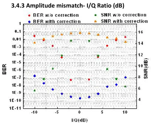
3.4.3 Amplitude mismatch- I/Q Ratio (dB)
Figure 3-6 BER and SNR vs. I/Q ratio for simulation single carrier QPSK. As shown in Figure 3-6, single carrier QPSK simulation results indicate that a 8dB amplitude mismatch corresponding to about 8 dB SNR degradation. However, after employing the Gram–Schmidt orthogonalization procedure (GSOP), substantial performance improvement is obtained. With a 8 dB amplitude mismatch, only about 1 dB SNR degradation is observed.
32
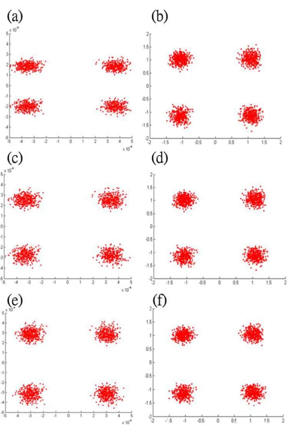
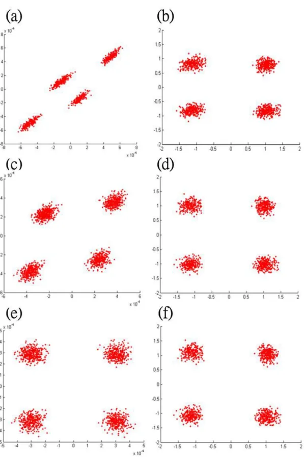
Figure 3-7 and Figure 3-9 show the constellations for simulation QPSK and
experimental QPSK amplitude mismatch with and without correction, respectively. Inset (a), (b), (c), (d), (e) and (f) of Figure3-7 and Figure 3-9 illustrate I/Q=8dB
Figure 3-7 Constellations for simulation QPSK amplitude mismatch w/ and w/o correction. (a) I/Q=8dB w/o correction (b) I/Q=8dB w/ correction (c) I/Q=4dB w/o correction
33
Figure 3-8 BER vs. I/Q ratio(Amplitude Mismatch) for experimental single carrier QPSK.
Figure 3-6 shows single carrier QPSK experimental results and indicates that a 8 dB amplitude mismatch corresponding to about 10 orders BER degradation. After employing the GSOP, substantial performance improvement is obtained. With a 8 dB
amplitude mismatch, only about 4 orders BER degradation is observed. And we can see that the curve trend is like simulation result.
34
Figure 3-9 Constellations for experimental QPSK amplitude mismatch w/ and w/o correction. (a) I/Q=8dB w/o correction (b) I/Q=8dB w/ correction (c) I/Q=4dB w/o correction
35
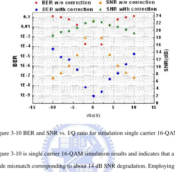
Figure 3-10 BER and SNR vs. I/Q ratio for simulation single carrier 16-QAM.
Figure 3-10 is single carrier 16-QAM simulation results and indicates that a 8 dB amplitude mismatch corresponding to about 14 dB SNR degradation. Employing the Gram–Schmidt orthogonalization procedure (GSOP), substantial performance
improvement is obtained, only about 3 dB SNR degradation is observed.
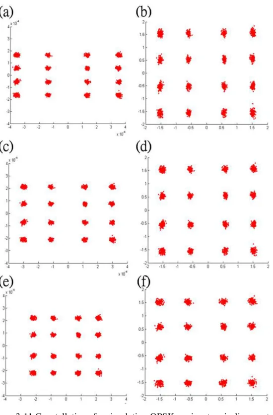
Figure 3-11 is the constellations for simulation 16-QAM amplitude mismatch with and without GSOP, respectively. Inset (a), (b), (c), (d), (e) and (f) of Figure3-11 illustrate I/Q=8dB without GSOP, I/Q=8dB with GSOP, I/Q=4dB without GSOP, I/Q=4dB with GSOP, I/Q=0dB without GSOP and I/Q=0dB with GSOP.
36
Figure 3-11 Constellations for simulation QPSK conjugate misalignment w/ and w/o GSOP. (a) I/Q=8dB w/o GSOP (b) I/Q=8dB w/ GSOP (c) I/Q=4dB w/o GSOP (d) I/Q=4dB w/ GSOP (e) I/Q=0dB w/o GSOP (f) I/Q=0dB w/ GSOP
37 3.4.4 Conjugate misalignment
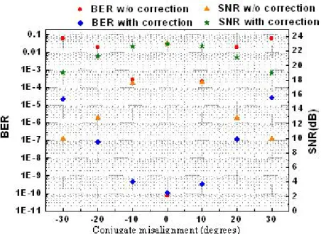
Figure 3-12 BER and SNR vs. conjugate misalignment for simulation single carrier QPSK.
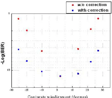
Figure 3-12 and Figure 3-14 show simulation and experimental results and indicate that a 30° conjugate misalignment corresponding to about 11 dB SNR and about 13 orders BER degradation, respectively. After employing the GSOP, substantial performance improvement is obtained. With a 30° conjugate misalignment, only about 3 dB SNR and 8 orders BER degradation are observed for simulation and experimental results, respectively.
38
Figure 3-13 Constellations for simulation QPSK conjugate misalignment w/ and w/o GSOP. (a) 30° w/o GSOP (b) 30° w/ GSOP (c) 10° w/o GSOP (d)10° w/ GSOP (e) 0° w/o GSOP (f) 0° w/ GSOP
39
Figure 3-14 BER vs. conjugate misalignment for experimental single carrier QPSK.
Figure 3-13 and Figure 3-15 are the constellations for simulation and
experimental 16-QAM conjugate misalignment with and without GSOP, respectively. Inset (a), (b), (c), (d), (e) and (f) of Figure3-13 and Figure3-15 illustrate 30° conjugate misalignment without GSOP, 30° conjugate misalignment with GSOP, 10° conjugate misalignment without GSOP, 10° conjugate misalignment with GSOP, 0° conjugate misalignment without GSOP and 0° conjugate misalignment with GSOP.
40
Figure 3-15 Constellations for experimental QPSK conjugate misalignment w/ and w/o GSOP. (a) 30° w/o GSOP (b) 30° w/ GSOP (c) 10° w/o GSOP (d)10° w/ GSOP (e) 0° w/o GSOP (f) 0° w/ GSOP
41
Figure 3-16 BER and SNR vs. conjugate misalignment for simulation single carrier 16-QAM.
Figure 3-16 is BER and SNR curves at different conjugate misalignment conditions for simulation 16-QAM and indicates that a 30° conjugate misalignment corresponding to about 12 dB SNR degradation. After employing the GSOP, only about 3 dB SNR degradation is observed.
Figure 3-17 shows the constellations for simulation 16-QAM conjugate
misalignment with and without GSOP. Inset (a), (b), (c), (d), (e) and (f) of Figure3-17 illustrate 30° conjugate misalignment without GSOP, 30° conjugate misalignment with GSOP, 10° conjugate misalignment without GSOP, 10° conjugate misalignment with GSOP, 0° conjugate misalignment without GSOP and 0° conjugate misalignment with GSOP.
42
Figure 3-17Constellations for simulation 16-QAM conjugate misalignment w/ and w/o GSOP. (a) 30° w/o GSOP (b) 30° w/ GSOP (c) 10° w/o GSOP (d)10° w/ GSOP
43
In order to resolve I/Q imbalance, the GSOP scheme is unitized to compensate the amplitude mismatch and conjugate misalignment. After employing GSOP scheme, the imbalance effects can be solved.
3.4.5 Synchronization
And now, I want to show you another imbalance factor - path length. If the lengths of data-I path and data-Q path are not exactly the same, the two data will not arrive at receiver at the same time. That may degrade the signal quality and distort signals.
We use VPI program and AWG to generate time delay effect. Figure3-18 and Figure 3-19 are BER and SNR curves at different time delay condition for simulation QPSK and experimental QPSK, respectively. Inset (a) and (b) of the two figures are
Figure 3-18 BER and SNR vs. Time Delay for simulation QPSK. (a) Time delay 50% w/o correction.
44
the constellations of time delay 50% without correction and with correction,
respectively. In these figures, we can obtain as data-I and data-Q delay a half cycle, the performance is worst. That is due to the judging points are far away. The two figures show results with correction and without correction. We find out utilizing off-line software correction will compensate the factor effect. We use Matlab program to shift judging points to make them the same. Now the two data seems arrive at the same time.
Figure 3-19 BER and SNR vs. Time Delay for experimental QPSK. (a)Time delay 50% w/o correction.
(b)Time delay 50% with correction.
Figure 3-20 shows results of simulation 16-QAM signals. The worst condition is also time delay 50%. After using correction, the signals are improved, too. Inset (a) and (b) of this illustrate constellations of time delay 50% without correction and with correction. Inset (a) constellation size is large, and inset (b) constellation is clear.
45
Figure 3-20 BER and SNR vs. Time Delay for simulation 16-QAM.
(c) Time delay 50% w/o correction. (d) Time delay 50% with correction.
46
Chapter4 Experimental demonstration of proposed system 4.1 Preface
In chapter 3, we discuss the influence on the proposed setup due to the imbalance-effect. And now, I want to show you the detail about the novel proposed experimental setup and the experimental outcome. In this chapter, we will build up the experimental setup for the proposed system based on SSBCS modulation. Figure 4-1(a), (b) and (c) show the comparison of different DD-OFDM modulation scheme.
4.2 Comparison of different DD-OFDM modulation scheme (a) Conventional SSB
47
4.2 Comparison of different DD-OFDM modulation scheme
Before showing the concept of the proposed system, we see the comparison of different DD-OFDM modulation scheme shown as Fig4-1. Conventionally, optical direct-detection OFDM (DD-OFDM) signal is generated based on single-sideband
(b) Virtual SSB
(c) Proposed System
Figure 4-1 Comparison of different DD-OFDM modulation shceme. (B: bandwidth of DAC, f0: optical carrier frequency, f0: intermedium