Enhanced efficiency in polymer light-emitting diodes due to the improvement of charge-injection balance
Yow-Jon Lina兲
Institute of Photonics, National Changhua University of Education, Changhua 500, Taiwan, Republic of China
Wei-Yang Chou and Shih-Ting Lin
Institute of Electro-Optical Science and Engineering, National Cheng Kung University, Tainan 701, Taiwan, Republic of China
共Received 22 August 2005; accepted 3 January 2006; published online 14 February 2006兲 The authors report the enhancement of efficiency of polymer light-emitting diodes共PLEDs兲 in the study. According to the experimental results, we find that PLEDs, fabricated on irradiated indium-tin-oxide surfaces by KrF excimer laser, with an organic layer between the cathode and the emitting layer may lead to the improvement of charge-injection balance and prevention of cathode metal quenching, resulting in a remarkable increase in external quantum efficiency. © 2006 American Institute of Physics. 关DOI:10.1063/1.2176856兴
Organic light-emitting diodes共OLEDs兲 or polymer light- emitting diodes共PLEDs兲 fabricated from organic functional materials have a large market potential in display and light- ing applications. Besides device technology development and some fundamental mechanistic question in OLEDs or PLEDs attract wide attention. Recent progress in OLEDs dates back to the early research of the 1950s.1It has taken 40 years for this technology to become commercialized.1 Ber- nanose first reported on electroluminescence in molecularly dispersed polymer films.2,3Efficiency is a key issue, not only for energy consumption, but also for its effect on the longev- ity of the devices, since the ability to operate a device at a lower input power at a given luminance共L兲 decreases Ohmic heating and increases device lifetime. Charge injection at the interface between metallic electrodes and organic semicon- ductors plays a crucial role in the performance of organic optoelectronic devices. Indium-tin oxide共ITO兲 has been the most common small-molecule OLED共or PLED兲 anode due to its high conductivity, high work function 共W兲, and high transparency.1,4–9At the interface of an ITO anode with or- ganic materials, enhanced hole injection was desired to inter- nal quantum efficiency共QE兲 by balancing charge carriers in the active layer. In a previous study,10 we found that KrF excimer laser irradiation is an effective treatment for enhanc- ing PLED performance, due to the increase in work function and the amount of oxygen on the ITO surfaces and the re- duction in ITO surface roughness, resulting in a reduction in leakage current at the organic layer/ITO interface and an increase in device luminance. However, laser irradiation re- sults in an increase in hole injection rate and does not affect electron injection. As pointed out by Parker,11 the energy barriers for electron and hole injections are both important, with the lower barrier determining device current and the higher one determining emission efficiency. In this letter, we report the enhancement of QE of PLEDs fabricated on irra- diated ITO surfaces by KrF excimer laser with the 4 , 4
⬘
-N , N⬘
-dicarbazole-biphenyl 共CBP兲 layer between the cath- ode and the emitting layer, due to the improvement ofcharge-injection balance and prevention of cathode metal quenching.
An ITO-coated glass 共Wintek Corp.兲 substrate was first cleaned by ultrasonic agitation in ethanol and subsequently in acetone followed by mechanical scrubbing in deionized water, again using a detergent. The ITO samples were then cleaned in an ultrasonic bath using a water solution of the same detergent and rinsed several times by ultrasonic agita- tion in water. The ITO samples were treated with an oven bake dry for 1 – 2 h and UV ozone for 9 min12 prior to the deposition of the polymer layers. Wu et al.13suggested that the removal of the organic residue from the cleaned ITO surface by the UV ozone treatment could be partially respon- sible for the device improvement. The luminescent polymer is a 100 nm green polyfluorene 共PF兲. Ca/Al 共60/120 nm兲 was used as the electron-injecting electrode 共cathode兲, vacuum evaporated on top of the polymer films. The final structure of the devices was ITO/ PEDOT/ PF/ Ca/ Al, re- ferred to as group A. On the other hand, the final structure of the devices was ITO/ PEDOT/ PF/ CBP/ Ca/ Al, referred to as group B. CBP共60 nm兲 was deposited on top of the PF films using physical vapor depositor. The CBP layer was inserted between the cathode and the emitting layer for PLEDs from group B, because the low work-function metal 共i.e., Ca兲 is highly reactive and tend to create detrimental quenching sites at areas near the interface between the cath- ode and the emitting layer, and current leakage.14In addition, we deduce that the insertion of the CBP layer in PLEDs may lead to the improvement of charge-injection balance and the increase in recombination rate of electron-hole pairs.15 The explanation for this will be given later. On the other hand, in order to enhance hole inject from ITO to organic materials, a KrF excimer laser was used to increase the work function of ITO.16 PLEDs 共structure: ITO/PEDOT/PF / CBP/ Ca/ Al兲 fabricated on irradiated ITO surfaces for 15 min by a KrF excimer laser were referred to as group C.
The I-V characteristics of the devices were measured with a Keithey-2400 source meter and L, with a Topcon BM-8 lu- minance meter. The emission area of each PLED was 2
⫻3 mm2.
a兲Author to whom correspondence should be addressed; electronic mail:
APPLIED PHYSICS LETTERS 88, 071108共2006兲
0003-6951/2006/88共7兲/071108/3/$23.00 88, 071108-1 © 2006 American Institute of Physics
Downloaded 22 Oct 2009 to 140.116.208.44. Redistribution subject to AIP license or copyright; see http://apl.aip.org/apl/copyright.jsp
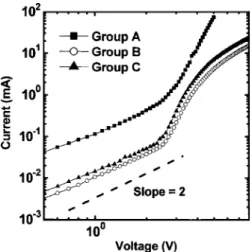
Figure 1 shows the I-V curves in forward bias for PLEDs from groups A, B, and C. The dependence of current on applied forward bias for semiconducting polymers has been explained with the space-charge limited current model.17,18 In Fig. 1, current of samples from group B is less than that of samples from group A. Tak and Bässler15found that current and QE of PLEDs may depend on the thickness共Le兲 of an organic layer 共i.e., hole-blocking layer or electron- conducting layer兲 between the cathode and the emitting layer and current increases with decreased Le. As a result, we de- duce that the insertion of the CBP layer in PLEDs may lead to the reduction in hole as well as the electron density stored at the interface per unit area and current.15 In addition, this may be also due to the overdoping of Ca in the emitting layer, resulting in an increase in leakage current for PLEDs from group A.14As a result, we deduce that many quenching sites form in the recombination and emission zone near the cathode during the metal evaporation, because of the absence of the CBP layer and the metal ion impact and implantation.14 In Fig. 1, we can also see that current of samples from group C is slightly greater than that of samples from group B. It is thought that holes were effectively in- jected from ITO to an organic layer, due to the increase in W of ITO, as well as the formation of a lower barrier at the organic layer/ITO interface. In a previous study,16we found that a KrF excimer laser irradiation might lead to the increase in W of ITO.
The L-V characteristics and external QE of PLEDs from groups A, B, and C are shown in Figs. 2 and 3, respectively.
The L-V characteristics at smaller voltages of PLEDs from group B are the same as that of PLEDs from group A. How- ever, the external QE of PLEDs from group B is larger than that of PLEDs from group A, due to prevention of cathode metal quenching and an increase in the overall recombina- tion yield as a result of the CBP layer. Tak and Bässler15 suggested that the reduction in Lein PLEDs might lead to an increase in hole as well as the electron density stored at the interface per unit area and at the same time carrier leakage became increasingly important. This causes the overall re- combination yield to decrease as the CBP layer is absent in the structure of PLEDs共i.e., Le= 0兲 while the absolute num- ber of recombination events increases because the overall current increases.15In other words, the electric field screen- ing at the anode for PLEDs from group A is less than that for PLEDs from group B, because of the absence of the CBP
layer in PLEDs from group A. This explains why the exter- nal QE of PLEDs from group B is larger than that of PLEDs from group A and current of PLEDs from group B is less than that of PLEDs from group A共shown in Figs. 1–3兲. On the other hand, in Fig. 2, we find that L-V characteristics at smaller voltages and external QE of PLEDs from group C are better than those of PLEDs from group B, which is at- tributed to the increase in recombination rate of electron-hole pairs as a result of KrF excimer laser irradiation共due to an increase in the ITO W and hole injection rate兲. In a previous study,19we found that W data observed using a Kelvin probe indicate homogeneous coverage for irradiated ITO samples by a KrF excimer laser, forming an almost metal-like Fermi level, resulting in a reduction in leakage current at the or- ganic layer/ITO interface. It is indeed necessary to minimize the leakage current to prevent unnecessary wasting of power and to increase external QE. Wu et al.13 demonstrated that ITO surface modification leads to good performance even in single-layer-polymer-based OLEDs, for which the ITO sur- face properties are more critical than in multilayer devices.
On the basis of experimental results, we deduce that laser irradiation and the insertion of the CBP layer in PLEDs strongly affect hole and electron injection, and the recombi- nation yield. Consequently, a corresponding increase in the number of electrons or holes leads to a dramatic increase in external QE of PLEDs, which is in good agreement with the reported result by Parker.11
In summary, we have demonstrated that the asymmetric charge injection may affect the internal and external QE of
FIG. 1. I-V curves in forward bias for PLEDs.
FIG. 2. L-V characteristics of PLEDs.
FIG. 3. External QE vs current for PLEDs.
071108-2 Lin, Chou, and Lin Appl. Phys. Lett. 88, 071108共2006兲
Downloaded 22 Oct 2009 to 140.116.208.44. Redistribution subject to AIP license or copyright; see http://apl.aip.org/apl/copyright.jsp
PLEDs. We find that the insertion of the CBP layer in PLEDs fabricated on nonirradiated ITO substrates may lead to an increase in the recombination efficiency and external QE, due to prevention of cathode metal quenching and an in- crease in the effect of electric field screening at the anode.
On the other hand, we find that the insertion of the CBP layer in PLEDs fabricated on irradiated ITO substrates by a KrF excimer laser may lead to the improvement of charge- injection balance and the prevention of cathode metal quenching, resulting in a drastic increase in external QE. The results are in good agreement with the prediction of an ana- lytic theory shown in Ref. 20.
The authors acknowledge support by grants from the Na- tional Science Council of Taiwan, Republic of China 共NSC93-2815-C-035-024-E and NSC94-2112-M-018-007兲.
1J. Shinar, Organic Light-Emitting Devices共Springer, Berlin, 2003兲.
2A. Bernanose, J. Chim. Phys. 51, 255共1954兲.
3A. Bernanose, J. Chim. Phys. 52, 396共1955兲.
4B. H. Cumpston and K. F. Jensen, Appl. Phys. Lett. 69, 3941共1996兲.
5S. M. Tadayyon, K. Griffiths, P. R. Norton, C. Tripp, and Z. Popovic, J.
Vac. Sci. Technol. A 17, 1773共1999兲.
6S. Y. Kim, J. L. Lee, K. B. Kim, and Y. H. Tak, Appl. Phys. Lett. 86, 133504共2005兲.
7I. M. Chan, T. Y. Hsu, and F. C. Hong, Appl. Phys. Lett. 81, 1899共2002兲.
8K. B. Kim, Y. H. Tak, Y. S. Han, K. H. Baik, M. H. Yoon, and M. H. Lee, Jpn. J. Appl. Phys., Part 2 42, L438共2002兲.
9P. W. M. Blom, M. J. M. de Jong, and J. J. M. Vleggaar, Appl. Phys. Lett.
68, 3308共1996兲.
10Y. J. Lin, W. Y. Chou, S. T. Lin, and Y. M. Chen, Jpn. J. Appl. Phys., Part 2 44, L1218共2005兲.
11I. D. Parker, J. Appl. Phys. 75, 1656共1994兲.
12C. Qiu, H. Chen, M. Wong, and H. S. Kwok, IEEE Trans. Electron Devices 48, 2131共2001兲.
13C. C. Wu, C. I. Wu, J. C. Sturm, and A. Kahn, Appl. Phys. Lett. 70, 1348 共1997兲.
14Y. H. Niu, H. Ma, Q. Xu, and A. K. Y. Jen, Appl. Phys. Lett. 86, 083504 共2005兲.
15Y. H. Tak and H. Bässler, J. Appl. Phys. 81, 6963共1997兲.
16Y. J. Lin, Y. M. Chen, and Y. C. Wang, J. Appl. Phys. 97, 083702共2005兲.
17M. A. Lampart and P. Mark, Current Injection in Solids共Academic, New York, 1970兲.
18P. Mark and W. Helfrich, J. Appl. Phys. 33, 205共1962兲.
19Y. J. Lin, I. D. Baikie, W. Y. Chou, S. T. Lin, H. C. Chang, Y. M. Chen, and W. F. Liu, J. Vac. Sci. Technol. A 23, 1305共2005兲.
20D. V. Khramtchenkov, V. J. Arkhipov, and H. Bässler, J. Appl. Phys. 81, 6954共1997兲.
071108-3 Lin, Chou, and Lin Appl. Phys. Lett. 88, 071108共2006兲
Downloaded 22 Oct 2009 to 140.116.208.44. Redistribution subject to AIP license or copyright; see http://apl.aip.org/apl/copyright.jsp