國立臺灣大學電機資訊學院電信工程學研究所 碩士論文
Graduate Institute of Communication Engineering College of Electrical Engineering and Computer Science
National Taiwan University Master Thesis
毫米波頻段放大器及功率放大器之共模穩定性研究
Research of Amplifiers and Common-mode Stability of Power Amplifiers at Millimeter-wave Frequencies
莊博翔
Po-Hsiang Chuang
指導教授﹕王暉 博士 Advisor: Huei Wang, Ph.D.
中華民國107年12月
December 2018
致謝
隨著論文的完成,我即將完成碩士學位,研究所生涯也將告一段落。首先,我要感謝我的指 導教授,王暉老師。一路以來對我無私的幫助,無論是在學術領域的研究上給予建議、方向,以 及寶貴的經驗,或是在問題解決上給予的指導與鼓勵,都使我有所成長。感謝林坤佑老師,在計 畫上的領導及幫助,以及給予我研究上的幫助,讓我解決許多問題。感謝蔡作敏老師、蔡政翰老 師,無論是在計畫上,以及研究上給予我無私的幫助及建議。同時,感謝天文所的章朝盛博士、
翁守賢博士及郭岳芳博士在研究上的幫助,以及提供天文所的量測環境,使研究能更加完整。感 謝口試委員們,黃天偉教授、林坤佑教授、蔡作敏教授、及蔡政翰教授所提供的建議,使得此碩 士論文能得以更加完整。
在研究所生涯中,學長姊、同學,以及學弟們的幫助,讓我有所成長也得以解決許多的問題。
博士班的學長姊中,感謝林毓軒學長、蕭元鴻學長、吳依靜學姊、陳俊年學長、王云杉學長、張 立奇學長、葉光聖學長、高堃堯學長、鄭人豪學長、吳茗航學長、林宜賢學長、林文傑學長,以 及鐘杰穎學長。碩士班的學長姊中,感謝周正峯學長、張育銓學長、陳柏羽學長、周昱廷學姊、
能繼康學長、林弘皓學長、吳振緯學長、王俊凱學長、區逸群學長、陳泓翰學長、許峰毓學長,
以及黃炫又學長。
碩士班同學中,感謝容麟、政宇、彥志、飛飛、碩軒、騰遠、宗瑾、俊名、紹庭,以及展鳴。
碩士班學弟中,感謝潁、洋、煒程、子兼、智尹、凱皇、柏澤、岱宥、彥廷、旻憲,以及武震。
最後,謝謝我摯愛的人們。謝謝家人的支持與鼓勵,謝謝夥伴及朋友們的陪伴,讓我得以順 利完成碩士學位。
博翔 2018.12.31
中文摘要
本論文介紹一個製作於砷化鎵假型高速電子場效電晶體製程之低雜訊放大器、一個製作 於互補式金屬氧化物半導體製程之開關鍵控調變器,以及一個製作於互補式金屬氧化物半導 體製程之功率放大器。
首先為一個應用於第五代行動通訊之 Q 頻段低雜訊放大器以 0.15 微米砷化鎵假型高速電 子場效電晶體製程設計與製作,此低雜訊放大器採用三級共源級的架構,第一共源級採用源 級衰退技術以達到均衡的雜訊及增益表現,而第二、三共源級則是採用 RC 回授技術以達到
寬頻表現,另外,放大器第三級前後之匹配網路採用 π 型匹配網路以達到寬頻的阻抗匹配。
在第一次實驗結果後,電晶體模型不準確導致量測與模擬結果的不一致,在進一步討論與分 析後提出模擬上的修正方法,修改晶片設計後再藉由第二次晶片製作及實驗結果驗證所提修 正方法之正確性。此低雜訊放大器放大器達到優異的 3-dB 頻寬(24.7 至 40.0 GHz)以及平均增 益(22.2 dB)表現,雜訊指數則在寬頻(27.9 至 40.0 GHz)下皆低於 3 dB。
之後描述一個應用於短距無線通訊之 60-GHz 頻段開關鍵控調變器以 90 奈米互補式金屬 氧化物半導體製程設計與製作,此調變器結合了發射機中調變以及輸出放大之功能,進而達 到在未來的應用上低複雜度與高效率的發射機架構。此調變器基於共源共柵架構,並採用在 此提出的一基於變壓器之回授技術,此技術能提升調變器「開」狀態下的增益及輸出功率表 現,以及「關」狀態下的隔離度表現,另外,為了降低基頻調變訊號輸入路徑上的 RC 常數 以減輕高速率傳輸下基頻調變訊號的失真,該路徑透過一串接電感及到地電容的設計以達到 所要目的。藉由採用基於變壓器之回授技術,此開關鍵控調變器於 60-GHz 達到優異的輸出 1-dB 功率壓縮點(7.0 dBm)、小訊號增益(10.2 dB)、以及「開-關」隔離度(45.4 dB)表現,在開 關鍵控調變上,此調變器能達到 10 Gb/s 之傳輸速率,由於變壓器所需的低佈局空間優勢,加 上僅需單一調變訊號輸入路徑,此調變器達到相當小的晶片佈局。
最後則討論一個應用於短距無線通訊之 W 頻段功率放大器以 65 奈米互補式金屬氧化物 半導體製程設計與製作,藉由於輸出端採用一基於變壓器之放射對稱功率結構,以達到低損 耗及阻抗匹配上的不平衡,此二項參數皆在極高頻的功率放大器設計上有相當大的重要性。
在第一次實驗後於毫米波頻段發現非預期的振盪現象,在討論以及多方面的穩定性分析後判 斷為共模訊號下位於輸出級的不穩定現象,並提出針對輸出級前後採用的變壓器設計的電路 修改方法,在不影響差動訊號下之阻抗匹配情況的前提下,消除共模訊號下之不穩定現象,
經過在第二次晶片製作,實驗顯示非預期振盪之問題已解決,並驗證所提出修改方法的正確 性。另外,亦討論了用於極高頻功率放大器電路設計時的變壓器模型問題。
關鍵字 – 砷化鎵假型高速電子場效電晶體、第五代行動通訊、低雜訊放大器、寬頻、Q 頻段、
互補式金屬氧化物半導體、開關鍵控調變、調變器、功率放大器、發射機、共柵共源、變壓 器回授、隔離度、60 GHz、V 頻段、功率結合結構、毫米波振盪現象、共源訊號不穩定現象、
W 頻段。
ABSTRACT
The thesis presents a GaAs pHEMT low noise amplifier, a CMOS on-off keying modulator, and a CMOS power amplifier.
Firstly, a Q-band low noise amplifier for fifth-generation communication applications is designed and realized in 0.15-μm GaAs pHEMT. The LNA consists of three common-source stages.
Source degeneration is adopted at the first stage for a balanced noise and gain performance, and RC-feedback is adopted at the latter two stages for its wideband characteristics. In addition, π-type matching networks are used at the third stage for wideband impedance matching. Inaccurate device modeling caused disagreement between the measurement and simulation results of the original LNA.
The modeling issues are discussed and analyzed, and corrections to the simulation setups are proposed and verified via the measurement results of a modified LNA in the second tape-out. The LNA exhibits wide 3-dB bandwidth from 24.7 to 40.0 GHz, with average gain of 22.2 dB. The noise figure is below 3 dB from 27.9 to 40.0 GHz, with average of 2.6 dB from 26 to 40 GHz.
Secondly, a 60-GHz OOK modulator for short range wireless communications is designed and realized in 90-nm CMOS. By combining the functions of modulation and output amplification in a single circuit, a transmitter of lower complexity and higher efficiency can be achieved for future applications. A novel transformer-feedback technique is proposed for the cascode-based modulator for improvements in output power, gain performances at on-state, and isolation performance at off-state. A data input network is designed to achieve low RC time constant, and avoids distortion of the baseband data signal at high data rates. With the proposed transformer-feedback technique, the modulator achieves an OP1dB of 7.0 dBm, gain of 10.2 dB, and on-off isolation of 45.4 dB at 60 GHz. For OOK modulation, data rates of up to 10 Gb/s have been measured. Due to the compact transformer and the single modulation path required, the modulator achieves a compact layout footprint of 471 x 519 μm2 with RF and DC pads included.
Finally, a W-band power amplifier is designed and realized in 65-nm CMOS. A transformer-based radial-symmetric power combining structure is adopted at the output for low insertion loss and matching imbalances, which are critical in PA designs at such high frequencies.
Undesired oscillations at millimeter-wave frequency were observed during measurement of the original PA. Discussions and various stability analyses are performed to identify the issue as common-mode instabilities at the output stage. Modifications to the transformers at the output stage are proposed in order to eliminate the common-mode instabilities, without altering the impedance matching conditions in differential mode. The proposed modifications are verified through the absence of undesired oscillations during the measurement of a modified PA in the second tape-out.
Modeling issues of high frequency transformer designs are also discussed.
Index Terms – GaAs pHEMT, fifth-generation (5G) communications, low noise amplifier, wideband, Q-band, CMOS, on-off keying (OOK), modulator, power amplifier, transmitter, cascode, transformer feedback, isolation, 60 GHz, V-band, power combining, millimeter-wave oscillation, common-mode instability, W-band.
CONTENTS
口試委員審定書...#
致謝...i
中文摘要...ii
ABSTRACT...iii
CONTENTS...vi
LIST OF FIGURES...ix
LIST OF TABLES...xxiii
Chapter 1 Introduction ... 1
1.1 Backgrounds and Motivations ... 1
1.2 Literature Surveys ... 4
1.2.1 Q-band LNA... 4
1.2.2 60-GHz OOK Modulator ... 6
1.2.3 W-band PA ... 7
1.3 Contributions ... 9
1.3.1 Q-band LNA in 0.15-μm GaAs pHEMT ... 9
1.3.2 60-GHz OOK Modulator in 90-nm CMOS ... 10
1.3.3 Common-mode stability of W-band PA in 65-nm CMOS ... 11
1.4 Thesis Organization ... 11
Chapter 2 A Q-band Low Noise Amplifier for Fifth-Generation Wireless Communication Receiver Applications in 0.15-μm GaAs pHEMT ... 13
2.1 Introduction ... 13
2.2 Circuit Design ... 15
2.2.1 Bias Condition and Device Selection ... 15
2.2.2 First Stage Design ... 20
2.2.3 Second and Third Stage Design with Wideband Performance ... 24
2.2.4 Simulation Results ... 28
2.3 Experimental Results ... 34
2.4 Discussion and Second Tape-out ... 38
2.4.1 Modeling Issue of Device with Source Degeneration ... 38
2.4.2 Design Modification and Second Tape-out... 43
2.4.3 Experimental Results ... 45
2.5 Summary ... 47
Chapter 3 A 60-GHz On-Off Keying Modulator with Transformer Feedback for Short Range Wireless Communications in 90-nm CMOS ... 51
3.1 Introduction ... 51
3.2 Transformer Feedback in Cascode-Based Circuits ... 53
3.2.1 On-state ... 54
3.2.2 Off-state ... 58
3.3 Circuit Design ... 62
3.3.1 Bias Condition and Device Selection ... 62
3.3.2 Transformer Design ... 66
3.3.3 In/Output Matching and Baseband Data Input Network ... 72
3.3.4 EM Simulation ... 72
3.3.5 Simulation Results ... 73
3.4 Experimental Results ... 85
3.4.1 On/Off-state Measurements ... 85
3.4.2 Modulation Measurements ... 98
3.5 Summary ... 104
Chapter 4 A Study on Common-mode stability of Millimeter-wave Power Amplifiers using a
W-band Design in 65-nm CMOS Process ... 107
4.1 Introduction ... 107
4.1.1 Transformer-based Power Combining ... 107
4.2 Circuit Design ... 112
4.2.1 Neutralization Technique ... 112
4.2.2 Device Selection and Output Stage Design ... 114
4.2.3 Second Driver Stage Design ... 123
4.2.4 First Driver Stage Design ... 129
4.2.5 Simulation Results ... 133
4.3 Experimental Results ... 138
4.4 Discussion and Second Tape-out ... 144
4.4.1 Common-Mode Instability ... 144
4.4.2 Design Modification ... 150
4.4.3 Transformer Test Circuit ... 163
4.4.4 Experimental Results ... 164
4.5 Summary ... 174
Chapter 5 Conclusions ... 177
REFERENCES...179
LIST OF FIGURES
Fig. 2.1. Simulated DC-IV curves of the device with gate periphery of 2f x 25 μm. ... 16 Fig. 2.2. Simulated gm and NFmin of the devices with different gate-periphery configurations versus VGS at VDS = 2.0 V. ... 17 Fig. 2.3. Simulated gm and IDS of the devices with different gate-periphery configurations versus VGS at VDS = 2.0 V. ... 17 Fig. 2.4. Simulated MSG/MAG and stability factor of the devices with different gate-periphery configurations at [VGS, VDS] = [0.6 V, 2.0 V]. ... 18 Fig. 2.5. Simulated NFmin of the devices with different gate-periphery configurations at [VGS, VDS]
= [0.6 V, 2.0 V]. ... 18 Fig. 2.6. Simulated Zopt of the devices with different gate-periphery configurations at [VGS, VDS]
= [0.6 V, 2.0 V]. ... 19 Fig. 2.7. Schematic of the proposed Q-band LNA. ... 19 Fig. 2.8. Simulated MSG/MAG and stability factor of the 2f x 25 μm device with different lengths of TLdeg’s. ... 21 Fig. 2.9. Simulated NFmin of the 2f x 25 μm device with different lengths of TLdeg’s. ... 22 Fig. 2.10. Simulated Zopt and Zin,conj of the 2f x 25 μm device with different lengths of TLdeg’s. .. 22 Fig. 2.11. Simulated S-parameters of the first stage complete with the input matching network. . 23 Fig. 2.12. Simulated noise figure of the first stage complete with the input matching network. ... 24 Fig. 2.13. Simulated MSG/MAG and stability factor of the 2f x 25 μm device with/without the proposed RC-feedback. ... 25 Fig. 2.14. Simulated NFmin of the 2f x 25 μm device with/without the proposed RC-feedback. ... 25 Fig. 2.15. Simulated S-parameters of the first and second stages complete with the input and inter-stage matching networks. ... 26
Fig. 2.16. Simulated noise figure of the first and second stages complete with the input and
inter-stage matching networks. ... 27
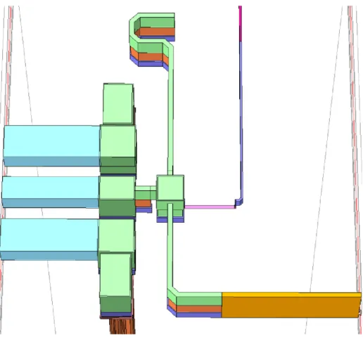
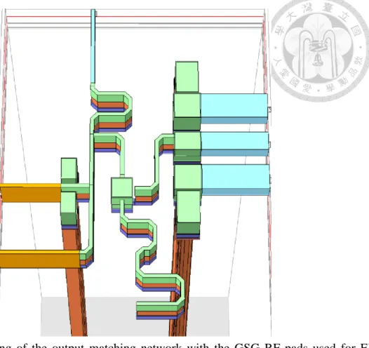
Fig. 2.17. 3-D rendering of the input matching network with the GSG RF pads used for EM simulation. ... 28
Fig. 2.19. 3-D rendering of the inter-stage matching network between the second and third stages used for EM simulation. ... 29
Fig. 2.18. 3-D rendering of the inter-stage matching network between the first and second stages used for EM simulation. ... 29
Fig. 2.20. 3-D rendering of the output matching network with the GSG RF pads used for EM simulation. ... 30
Fig. 2.22. Simulated noise figure of the proposed Q-band LNA... 31
Fig. 2.21. Simulated S-parameters of the proposed Q-band LNA. ... 31
Fig. 2.23. Simulated stability factor of the proposed Q-band LNA. ... 32
Fig. 2.24. Simulated inter-stage stability analyses between the first and second stages, with (a) load stability circles of N1 compared with 2-to-1 mapped circles of N2, and (b) source stability circles of N2 compared with 1-to-2 mapped circles of N1. ... 33
Fig. 2.25. Simulated inter-stage stability analyses between the second and third stages, with (a) load stability circles of N1 compared with 2-to-1 mapped circles of N2, and (b) source stability circles of N2 compared with 1-to-2 mapped circles of N1. ... 33
Fig. 2.26. Die photograph of the proposed Q-band LNA. ... 34
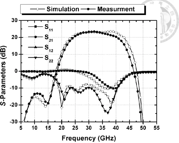
Fig. 2.27. Measured and simulated S-parameters of the proposed Q-band LNA. ... 35
Fig. 2.28. Measured and simulated noise figure of the proposed Q-band LNA. ... 36
Fig. 2.30. Measured and simulated S-parameters of the third stage test circuit. ... 37
Fig. 2.29. Measured and simulated S-parameters of the first stage test circuit. ... 37
Fig. 2.31. Die photograph of the test-key for the 2f x 25 μm CPW-configuration device with 85 x 20 μm TLdeg’s. ... 38 Fig. 2.32. Simulation setup for CPW-configuration devices with TLdeg’s in Agilent ADS. ... 39 Fig. 2.33. Measured and simulated magnitudes (in dB) of the S-parameters of the 2f x 25 μm CPW-configuration device with 85 x 20 μm TLdeg’s. ... 40 Fig. 2.34. Measured and simulated phases of the S-parameters of the 2f x 25 μm CPW-configuration device with 85 x 20 μm TLdeg’s. ... 40 Fig. 2.35. Measured and simulated S-parameters of the proposed LNA. The measurement results of the test-key is used as the device at the first stage in the simulation, instead of the foundry-provided measurement data. ... 41 Fig. 2.36. Measured and simulated magnitudes (in dB) of the S-parameters of the 2f x 25 μm CPW-configuration device with 85 x 20 μm TLdeg’s. Length of the TLdeg’s in simulation is shortened by 60 μm to 25 μm. ... 42 Fig. 2.37. Measured and simulated phases of the S-parameters of the 2f x 25 μm CPW-configuration device with 85 x 20 μm TLdeg’s. Length of the TLdeg’s in simulation is shortened by 60 μm to 25 μm. ... 42 Fig. 2.38. Measured and simulated S-parameters of the proposed LNA, with the proposed correction applied in the simulation. ... 43 Fig. 2.39. Post-EM simulated S-parameters of the modified LNA with the proposed correction. . 44 Fig. 2.40. Post-EM simulated noise figure of the modified LNA with the proposed correction. ... 44 Fig. 2.41. Measured and simulated S-parameters of the modified LNA, with the proposed correction applied in the simulation. ... 46 Fig. 2.42. Measured and simulated noise figure of the modified LNA, with the proposed correction applied in the simulation. ... 47
Fig. 3.1. Schematic of the proposed cascode-based transformer feedback technique. ... 53 Fig. 3.2. Small-signal equivalent circuit models of a cascode circuit at on-state (a) without and (b) with the proposed transformer feedback. ... 54 Fig. 3.3. Simulated (a) MSG/MAG and (b) stability factor of the cascode circuit with different configurations of the transformer. ... 57 Fig. 3.4. Small-signal equivalent circuit models of a cascode structure at off-state. ... 58 Fig. 3.5. Small-signal equivalent circuit model of a cascode structure at off-state with the proposed transformer feedback. ... 59 Fig. 3.6. Simulated phase difference between node S2 and G2 versus different Pin levels at 60-GHz. ... 60 Fig. 3.7. Simulated signal power at S2 and G2 (in dBm) versus different Pin levels at 60-GHz. . 60 Fig. 3.8. Simulated signal magnitude at the output node (in dBm) at 60-GHz. ... 61 Fig. 3.9. Simulated MSG/MAG of a cascode circuit at off-state with different transformer coupling coefficients. ... 61 Fig. 3.10. Schematic of the proposed OOK modulator. ... 62 Fig. 3.11. Simulated DC-IV curves of the cascode circuit with two identical device gate peripheries of 20f x 2 μm. ... 64 Fig. 3.12. Simulated gm and IDS of a 20f x 2μm device in common-source configuration versus different VGS at VDS = 1.0V. ... 64 Fig. 3.13. Simulated MSG/MAG and stability factor of the cascode circuit with different configurations of a total 40 μm gate-periphery. ... 65 Fig. 3.14. Simulated MSG/MAG of the cascode circuit at on-state with fixed Ls = 60 pH and varying Lg2 from 40 to 100 pH. ... 67
Fig. 3.15. Simulated stability factor the cascode circuit at on-state with fixed Ls = 60 pH and
varying Lg2 from 40 to 100 pH. ... 67
Fig. 3.16. Simulated MSG/MAG of the cascode circuit at on-state with fixed Lg2 = 60 pH and varying Ls from 40 to 100 pH... 68
Fig. 3.17. Simulated stability factor of the cascode circuit at on-state with fixed Lg2 = 60 pH and varying Ls from 40 to 100 pH... 68
Fig. 3.18. Simulated MSG/MAG of the cascode circuit at off-state with fixed Ls = 60 pH and varying Lg2 from 40 to 100 pH. ... 69
Fig. 3.19. Simulated MSG/MAG of the cascode circuit at on-state with fixed Lg2 = 60 pH and varying Ls from 40 to 100 pH... 69
Fig. 3.20. Post-EM simulated parameters of the feedback transformer. ... 70
Fig. 3.21. Post-EM simulated MSG/MAG and stability factor of the cascode circuit with transformer feedback at on-state. ... 71
Fig. 3.22. Post-EM simulated MSG/MAG of the cascode circuit with transformer feedback at off-state. ... 71
Fig. 3.23. 3-D rendering of the area around the devices used for EM simulation. ... 73
Fig. 3.24. Simulated S-parameters of the proposed modulator at on-state. ... 74
Fig. 3.25. Simulated S-parameters of the proposed modulator at off-state. ... 74
Fig. 3.26. Simulated large-signal performances of the proposed modulator at 60 GHz at on-state. .. ... 76
Fig. 3.27. Simulated large-signal performances of the proposed modulator at on-state versus frequency. ... 77
Fig. 3.28. Simulated large-signal performances of the proposed modulator at 60 GHz at off-state. . ... 77
Fig. 3.29. Simulated stability factor of the proposed modulator at on-state. ... 78
Fig. 3.30. Simulated drain current (IDD) and power consumption (PDC) at on-state versus Pin. ... 78
Fig. 3.31. Simulated output (a) spectrum and (b) waveform of the modulated signal at data rate of 4.5 Gb/s. ... 79
Fig. 3.32. Simulated output (a) spectrum and (b) waveform of the modulated signal at data rate of 6 Gb/s. ... 80
Fig. 3.33. Simulated output (a) spectrum and (b) waveform of the modulated signal at data rate of 8 Gb/s. ... 81
Fig. 3.34. Simulated output (a) spectrum and (b) waveform of the modulated signal at data rate of 10 Gb/s. ... 82
Fig. 3.35. Simulated eye pattern of the OOK modulation at data rate of 4.5 Gb/s. ... 83
Fig. 3.36. Simulated eye pattern of the OOK modulation at data rate of 6 Gb/s. ... 83
Fig. 3.37. Simulated eye pattern of the OOK modulation at data rate of 8 Gb/s. ... 84
Fig. 3.38. Simulated eye pattern of the OOK modulation at data rate of 10 Gb/s. ... 84
Fig. 3.39. Die photograph of the proposed OOK modulator. ... 85
Fig. 3.40. Measured and simulated S-parameters of the proposed modulator at on-state. ... 87
Fig. 3.41. Measured and simulated S-parameters of the proposed modulator at off-state. ... 87
Fig. 3.42. Measured and simulated large-signal performances of the proposed modulator at on-state at 60 GHz... 88
Fig. 3.43. Measured and simulated large-signal performances of the proposed modulator at on-state at 50 GHz... 88
Fig. 3.44. Measured and simulated large-signal performances of the proposed modulator at on-state at 52 GHz... 89
Fig. 3.45. Measured and simulated large-signal performances of the proposed modulator at on-state at 54 GHz... 89
Fig. 3.46. Measured and simulated large-signal performances of the proposed modulator at on-state at 56 GHz... 90 Fig. 3.47. Measured and simulated large-signal performances of the proposed modulator at on-state at 58 GHz... 90 Fig. 3.48. Measured and simulated large-signal performances of the proposed modulator at on-state at 62 GHz... 91 Fig. 3.49. Measured and simulated large-signal performances of the proposed modulator at on-state at 64 GHz... 91 Fig. 3.50. Measured and simulated large-signal performances of the proposed modulator at on-state at 66 GHz... 92 Fig. 3.51. Measured and simulated large-signal performances of the proposed modulator at on-state versus frequency. ... 92 Fig. 3.52. Measured and simulated large-signal performances of the proposed modulator at off-state at 60 GHz. ... 93 Fig. 3.53. Measured and simulated S-parameters of the proposed modulator at on-state with VG2,on
= 1.6 V . ... 95 Fig. 3.54. Measured and simulated S-parameters of the proposed modulator at on-state with VG2,on
= 1.4 V. ... 95 Fig. 3.55. Measured and simulated S-parameters of the proposed modulator at on-state with VG2,on
= 1.2 V. ... 96 Fig. 3.56. Measured and simulated large-signal performances of the proposed modulator versus frequency with VG2,on = 1.6 V. ... 96 Fig. 3.57. Measured and simulated large-signal performances of the proposed modulator versus frequency with VG2,on = 1.4 V. ... 97
Fig. 3.58. Measured and simulated large-signal performances of the proposed modulator versus
frequency with VG2,on = 1.2 V. ... 97
Fig. 3.59. Setup for modulation measurements in frequency-domain... 99
Fig. 3.60. Measured output spectrum of the modulated signal at data rate of 4.5 Gb/s. ... 99
Fig. 3.61. Measured output spectrum of the modulated signal at data rate of 6 Gb/s. ... 100
Fig. 3.62. Measured output spectrum of the modulated signal at data rate of 8 Gb/s. ... 100
Fig. 3.63. Measured output spectrum of the modulated signal at data rate of 10 Gb/s. ... 101
Fig. 3.64. Setup for modulation measurements in time-domain. ... 101
Fig. 3.65. Measured output waveform of the modulated signal at data rate of 4.5 Gb/s... 102
Fig. 3.66. Measured output waveform of the modulated signal at data rate of 6 Gb/s... 102
Fig. 3.67. Measured output waveform of the modulated signal at data rate of 8 Gb/s... 103
Fig. 3.68. Measured output waveform of the modulated signal at data rate of 10 Gb/s... 103
Fig. 4.1. Commonly used power combining structures: (a) binary power combining (b) transformer-based power combining. ... 108
Fig. 4.2. Schematics of (a) voltage-combining configuration, and (b) current-combining configuration of transformer-based power combining. ... 109
Fig. 4.3. Schematics of (a) voltage-combining configuration, and (b) current-combining configuration of transformer-based power combining, with the parasitic capacitances considered. ... 111
Fig. 4.4. Schematic of neutralization technique implementation in differential mode with cross-coupled capacitors between device gate and drain. ... 113
Fig. 4.5. Schematic of the output stage complete with the four-way transformer-based power combiner. ... 113
Fig. 4.6. Simulated DC-IV curves of the device with gate-periphery of 32f x 1 μm. ... 115
Fig. 4.7. Simulated gm and IDS of the 32f x 1μm device versus VGS at VDS = 1.2 V. ... 115
Fig. 4.8. Simulated MSG/MAG and stability factor of a single 32f x 1 μm device compared with two parallel-combined 16f x 1 μm devices. ... 116 Fig. 4.9. Schematic of the output stage differential pair with four 16f x 1 μm devices. ... 116 Fig. 4.10. Simulated MSG/MAG and stability factor of the output differential pair at 110 GHz versus different values of CN. ... 117 Fig. 4.11. Post-EM simulated MSG/MAG and stability factor of the output differential pair. .... 118 Fig. 4.12. Post-EM simulated power contours of the output differential pair. ... 118 Fig. 4.13. 3-D rendering of the output transformer TFout used for EM simulation. ... 119 Fig. 4.14. Post-EM simulated parameters of the output transformer TFout. ... 119 Fig. 4.15. Post-EM simulated S-parameters of the four-way transformer-based power combiner. ....
... 120 Fig. 4.16. Simulated S-parameters of the output stage complete with the four-way transformer-based power combiner. ... 121 Fig. 4.17. Simulated large-signal performance at 110 GHz of the output stage complete with the four-way transformer-based power combiner. ... 122 Fig. 4.18. Simulated large-signal performances versus frequency of the output stage complete with the four-way transformer-based power combiner. ... 122 Fig. 4.19. Schematic of the second driver and output stages complete with the inter-stage matching network. ... 123 Fig. 4.20. Simulated MSG/MAG and stability factor of the second driver stage differential pair at 110 GHz versus different values of CN. ... 124 Fig. 4.21. Post-EM simulated MSG/MAG and stability factor of the second driver stage differential pair. ... 124 Fig. 4.22. Post-EM power contours of the second driver stage differential pair. ... 125 Fig. 4.23. 3-D rendering of the inter-stage transformer TFinter2 used for EM simulation. ... 126
Fig. 4.24. Post-EM simulated parameters of the inter-stage transformer TFinter2. ... 126
Fig. 4.25. Simulated S-parameters of the second driver and output stages complete with the inter-stage matching network and output transformer-based power combiner. ... 127
Fig. 4.26. Simulated large-signal performances at 110 GHz of the second driver and output stages complete with the inter-stage matching network and output transformer-based power combiner. ... 128
Fig. 4.27. Simulated large-signal performances versus frequency of the second driver and output stages complete with the inter-stage matching network and output transformer-based power combiner. ... 128
Fig. 4.28. Schematic of the first and second driver stages complete with the inter-stage matching network... 129
Fig. 4.29. 3-D rendering of the inter-stage transformer TFinter1 used for EM simulation. ... 130
Fig. 4.30. Post-EM simulated parameters of the inter-stage transformer TFinter1. ... 130
Fig. 4.31. Schematic of the proposed W-band PA. ... 131
Fig. 4.32. 3-D rendering of the input transformer TFin used for EM simulation. ... 132
Fig. 4.33. Post-EM simulated parameters of the input transformer TFin. ... 132
Fig. 4.34. Simulated S-parameters of the proposed W-band PA. ... 134
Fig. 4.35. Simulated large-signal performance at 110 GHz of the proposed W-band PA. ... 134
Fig. 4.36. Simulated large-signal performance at 106 GHz of the proposed W-band PA. ... 135
Fig. 4.37. Simulated large-signal performance at 108 GHz of the proposed W-band PA. ... 135
Fig. 4.38. Simulated large-signal performance at 112 GHz of the proposed W-band PA. ... 136
Fig. 4.39. Simulated large-signal performance at 114 GHz of the proposed W-band PA. ... 136
Fig. 4.40. Simulated large-signal performances versus frequency of the proposed W-band PA. . 137
Fig. 4.41. Simulated IDS of each stage versus Pin at 110 GHz of the proposed W-band PA. ... 137
Fig. 4.42. Simulated stability factor of the proposed W-band PA. ... 138
Fig. 4.43. Chip layout of the proposed W-band PA. ... 139 Fig. 4.44. Measured and simulated S-parameters of the proposed W-band PA. ... 140 Fig. 4.45. Measured and simulated large-signal performance of the proposed W-band PA at 96 GHz. ... 141 Fig. 4.46. Measured and simulated large-signal performance of the proposed W-band PA at 92 GHz. ... 141 Fig. 4.47. Measured and simulated large-signal performance of the proposed W-band PA at 94 GHz. ... 142 Fig. 4.48. Measured and simulated large-signal performance of the proposed W-band PA at 98 GHz. ... 142 Fig. 4.49. Measured and simulated large-signal performance of the proposed W-band PA at 100 GHz. ... 143 Fig. 4.50. Output spectrum of the proposed W-band PA showing an undesired oscillation at 47.24 GHz. ... 145 Fig. 4.51. Schematic of the simulation for bias-line stability analysis on the output stage. ... 146 Fig. 4.52. Simulated stability factors from the two cases of bias-line analysis. ... 146 Fig. 4.53. Schematic of the simulation for the common-mode stability analysis of the output stage.
... 147 Fig. 4.54. Simulated stability factor of the common-mode stability analysis of the output stage. ...
... 148 Fig. 4.55. Schematic of the simulation for the common-mode stability analysis of the output stage using stability circles. ... 148 Fig. 4.56. Simulated stability circles from the common-mode stability analysis of the output stage.
... 149
Fig. 4.57. Top views of the 3-D renderings of the inter-stage transformer TFinter2 (a) before and (b) after the proposed modification. ... 150 Fig. 4.58. Post-EM simulated S-parameters in common mode of the inter-stage transformer TFinter2 in (a) dB and (b) phase with/without the proposed modification. ... 152 Fig. 4.59. Post-EM simulated S-parameters in differential mode of the inter-stage transformer TFinter2 in (a) dB and (b) phase with/without the proposed modification. ... 153 Fig. 4.60. Post-EM simulated loss of the inter-stage transformer TFinter2 using MSG/MAG in (a) common mode and (b) differential mode with/without the proposed modification. ... 154 Fig. 4.61. Post-EM simulated stability circles from the common-mode stability analysis of the output stage after the proposed modification to TFinter2. ... 155 Fig. 4.62. Top views of the 3-D renderings of the output transformer TFout (a) before and (b) after the proposed modification. ... 155 Fig. 4.63. Post-EM simulated S-parameters in common mode of the output transformer TFout in (a)
dB and (b) phase with/without the proposed modification. ... 157 Fig. 4.64. Post-EM simulated S-parameters in differential mode of the output transformer TFout in (a) dB and (b) phase with/without the proposed modification. ... 158 Fig. 4.65. Post-EM simulated stability circles from the common-mode stability analysis of the output stage after the proposed modifications to TFinter2 and TFout. ... 159 Fig. 4.65. Simulated stability factor of the common-mode stability analysis of the output stage after the proposed modifications to TFinter2 and TFout. ... 160 Fig. 4.67. Simulated stability factors from the two cases of bias-line analysis after the proposed modifications to TFinter2 and TFout. ... 160 Fig. 4.68. Simulated S-parameters of the proposed W-band PA before (first tape-out) and after (second tape-out) the modifications. ... 161
Fig. 4.69. Simulated large-signal performance of the proposed W-band PA at 110 GHz before (first tape-out) and after (second tape-out) the modifications. ... 161 Fig. 4.70. Simulated common-mode MSG/MAG and stability factor of the output differential cell with/without CN... 162 Fig. 4.71. 3-D renderings of the three components of the transformer test circuit: (a) TEST_CIRCUIT, (b) OPEN, and (c) SHORT. ... 162 Fig. 4.72. Basic concept of open-short de-embedding, with circuit schematics of (a) DUT, (b) SHORT, and (c) OPEN. ... 164 Fig. 4.73. Measured and simulated S-parameters of the modified PA in the second tape-out. .... 166 Fig. 4.74. Measured S-parameters of the modified and original PA in the two tape-outs. ... 166 Fig. 4.75. Measured and simulated large-signal performance of the modified PA in the second tape-out at 98 GHz. ... 167 Fig. 4.76. Measured and simulated large-signal performance of the modified PA in the second tape-out at 92 GHz. ... 168 Fig. 4.77. Measured and simulated large-signal performance of the modified PA in the second tape-out at 94 GHz. ... 168 Fig. 4.78. Measured and simulated large-signal performance of the modified PA in the second tape-out at 96 GHz. ... 169 Fig. 4.79. Measured and simulated large-signal performance of the modified PA in the second tape-out at 100 GHz. ... 169 Fig. 4.80. Measured and simulated large-signal performance of the modified PA in the second tape-out at 102 GHz. ... 170 Fig. 4.81. Measured and simulated large-signal performances versus different frequencies of the modified PA in the second tape-out. ... 170 Fig. 4.82. 3-D rendering of the transformer test circuit (DUT only) used for EM simulation. .... 171
Fig. 4.83. Measured and simulated magnitude (in dB) of the S-parameters of the transformer test circuit. ... 172 Fig. 4.84. Measured and simulated phase of the S-parameters of the transformer test circuit. .... 172 Fig. 4.85. 3-D rendering of the output transformer-based power combiner of the modified PA used for EM simulation. ... 173
LIST OF TABLES
Table 1.1. Previously reported K- and Q-band LNA designs. ... 5 Table 1.2. Previously reported CMOS OOK modulators. ... 7 Table 1.3. Previously reported W-band PA designs in CMOS processes... 9 Table 2.1. Target performances for the proposed Q-band LNA. ... 13 Table 2.1. Target performances for the proposed Q-band LNA. ... 14 Table 2.2. Bias conditions during small-signal measurements of the proposed Q-band LNA. ... 34 Table 2.3. Bias conditions during small-signal measurements of the proposed Q-band LNA. ... 45 Table 2.4. Previously Reported K- and Q-band LNA designs. ... 50 Table 3.1. Target performance of the proposed modulator. ... 63 Table 3.2. Bias conditions during on/off-state small-signal measurements. ... 86 Table 3.3. Bias conditions during on/off-state small-signal measurements (continued). ... 94 Table 3.4. Previously Reported OOK Modulator Designs in CMOS processes. ... 106 Table 4.1. Bias conditions during small-signal measurements. ... 139 Table 4.2. Bias conditions during small-signal measurements. ... 164 Table 4.3. Previously Reported W-band PA Designs in CMOS processes. ... 176
Chapter 1 Introduction
1.1 Backgrounds and Motivations
The fifth generation (5G) wireless communication has been the focus of interests in recent years. Compared to the current fourth generation long-term evolution (4G-LTE) configuration, 5G promises at least a tenfold increase in data rate, reaching the multi-Gb/s levels [1]-[2]. Higher carrier frequency bands, e.g., 28 GHz, 38 GHz, 60 GHz, etc., stood out as potential candidates as the required available bandwidth increase beyond 1 GHz. Under the same fractional bandwidth (FBW), a wider available bandwidth comes with having a higher carrier frequency. Furthermore, higher frequency bands lead to other benefits such as smaller physical footprints for the antenna and circuit components. The high free space loss and extra loss due to the oxygen absorbance peak at the 60-GHz band limit its applications to short-range, multi-Gb/s, device-to-device communications.
The 38-GHz band is a valid candidate for 5G communication receiver applications.
As often the first component after the receiving antenna, the gain and noise figure performances of the LNA dominate the signal-to-noise ratio (SNR) of the overall receiver. III-V compound semiconductor technologies are often used in LNA designs for the high gain and low noise performances. GaAs-based HEMT has been a stable and mature technology for microwave applications with relatively low cost for the performance it provides. LNA designs using GaAs-based HEMT processes have been reported for satellite communications and radio astronomy applications [3]-[8], in which high sensitivity and good noise performance of the receiver are required. In chapter 2, a Q-band LNA with source degeneration and RC-feedback techniques for a balanced gain, low noise, and wideband performance in 0.15-μm GaAs pHEMT will be introduced.
In recent years, the demand for high data rates in wireless communications has brought increasing interests towards millimeter-wave frequencies. The 60-GHz band has stood out thanks to its wide unlicensed band. A wide available bandwidth means that multi-Gb/s communication is
achievable even under the most basic, spectrally inefficient modulation schemes such as on-off keying (OOK). This result in a transceiver system with low complexity and DC power consumption, which is well suited for the short-range, multi-Gb/s communication applications targeted at mobile devices [21]-[28].
Switching-amplifier configuration of an OOK modulator operates by switching the output amplifier on/off in accordance with the baseband data signal [21]-[23], [32]-[33]. Modulation and amplification are performed by the same circuit, which only consumes DC power at on-states. This result in a transmitter of low DC power consumption and complexity. Critical performances of switching-amplifier configuration modulators are output power, gain, on-off isolation, and maximum data rate. Cascode circuit is commonly used for the switching-amplifier configuration.
Modulation is performed by switching the gate bias of the common-gate device. However, due to leakage of the devices, cascode-based modulators often suffers from low on-off isolation. For OOK transmitters, higher SNR at the receiver end can be achieved by either increasing the output power, or minimizing leakage at off-state while maintaining gain at on-state, i.e., increasing on-off isolation.
With the former often leads to high DC power consumption, improvement in on-off isolation is commonly pursued [22]-[28], [32]-[36]. In chapter 3, a 60-GHz cascode-based OOK modulator design with transformer feedback technique in 90-nm CMOS will be introduced. The technique improves the output power, gain performances at on-state, and isolation performance at off-state.
Wireless communications in millimeter-wave frequencies gain many interests in recent years due to the large available bandwidth and therefore higher data rates [39]-[47], [50]. Wireless systems designed at W-band benefit from having smaller circuit footprints and antenna sizes, with the short wavelength also provides potentials for imaging applications in area such as bio-medical research. Advanced nanoscale technologies such as 28, 40, and 65-nm CMOS processes have the advantage of higher gain and fmax/fT, which are especially critical in amplifier designs at millimeter-wave frequencies. However, shorter gate-lengths lead to lower breakdown voltages,
which in turn limit the supply voltage. This poses challenges to PA designs in achieving high levels of output power. Power combining is widely used for increasing the output power under low supply voltages [47]-[50]. Due to the short wavelength at millimeter-wave frequencies, the phase difference between combining paths becomes highly sensitive to any physical asymmetry of the power combining structure. Phase difference between combining paths degrades the combined power, and therefore the amplifier efficiency.
Binary power combining uses transmission lines for the purposes of both in-phase power combining and impedance matching. A wideband performance can often be achieved with careful design of the transmission lines [44]-[46], [50]. However, a large transformation ratio between the optimal impedance of the devices and the load impedance leads to longer transmission lines, and therefore higher insertion losses. Furthermore, transmission lines often take up large layout footprint, even at millimeter-wave frequencies. Transformer-based power combining has stood out in millimeter-wave PA designs recently [39], [48]-[49]. Transformers also serves the purposes of both in-phase power combining and impedance matching, but in a much more compact layout footprint than transmission lines. Since a large impedance transformation ratio does not necessarily translate to a large insertion loss of the transformer, the technique is especially suited for multi-way, high output power PA designs. In chapter 3, a W-band PA with a transformer-based, four-way, radial-symmetric power combining structure adopted at the output for low insertion loss and matching imbalances in 65-nm CMOS will be introduced.
1.2 Literature Surveys 1.2.1 Q-band LNA
The gain and noise figure are the most critical performances of a LNA design. III-V compound semiconductor technologies are often used in LNA designs for the high gain and low noise performances. LNA designs using GaAs-based HEMT processes have been reported for satellite communications and radio astronomy applications [21]-[26], in which high sensitivity and good noise performance of the receiver are required. Table 1.1 summarizes the previously reported K- and Q-band LNA designs.
The LNA in [21] uses π-type matching network and compensated matching to achieve wideband performance. The LNAs in [22]-[26], [29], [32] show great gain and noise performance due to process advantages in 0.1-μm GaAs pHEMT, GaAs mHEMT, and InP HEMT. The LNAs in [28] and [31] show gain and low noise performances, but are narrowband designs. The low noise medium power amplifier (LNMPA) in [30] shows good gain, low noise, and wideband performances, but requires high DC power consumption for the output power performance. The 90-nm CMOS LNA in [33] shows low DC power consumption, but gain and noise performances are still inferior to LNAs in III-V compound semiconductor technologies.
In chapter 3, the proposed LNA is designed in 0.15-μm GaAs pHEMT process for its excellent device performances and low loss characteristics of passive components. Source degeneration, RC-feedback, and π-type matching network are used for high gain, low noise, and wideband performances.
Table 1.1. Previously Reported K- and Q-band LNA designs.
Ref. Technology Freq.
(GHz)
FBW (%)
Gain (dB)
Noise Figure
(dB)
PDC
(mW)
Area (mm2) [3] 0.15-μm GaAs
pHEMT 28.5-50.5 56 23 3.8 62.6 2x1.5
[4] 0.1-μm GaAs
pHEMT 18.5-30 47 29 2.1 27 2x1
[5] 0.1-μm GaAs
pHEMT 27-45 50 25 2.9 9 2x1
[6] 50-nm GaAs
mHEMT 25-60 84 27.5 1.85 60 2x1
[7] 0.15-μm GaAs
mHEMT 27.3-50.7 60 23.1 3.7 88 2x2
[8]
0.15-μm GaAs
mHEMT 37-53.2 36 32.5 3.21 152 2x1
0.15-μm GaAs
mHEMT 32-50 44 29.5 2.8 140 2x1
[9] 0.12-μm GaN
HEMT 33-41 22 15 3 280 1x0.7
[10] 0.1-μm GaAs
HEMT 43-45 4.5 28 2.9 24 3.6x1.8*
[11] 0.2-μm InP HEMT 23-49 72 11 2.5 10 2.3x1.5
[12] 0.15-μm GaAs
pHEMT 24-40 50 24 2.1 520 1.5x2.8
[13] 0.15-μm GaN
T-gate DHFET 42-47 11 22 3.5 140 2.5x1.3
[14] 0.1-μm GaAs
pHEMT 18-43 82 21.6 2.3 140 2x1
[15] 90-nm CMOS 30-42 33 18 5 18 0.6x0.48
1.2.2 60-GHz OOK Modulator
Table 1.2 summarizes the previously reported silicon-based OOK modulator designs. Three configurations of an OOK transmitter are commonly used. In a switching-oscillator configuration, the oscillator is switched on/off in accordance with the baseband data signal [29]-[30]. Since there is no carrier signal generated at off-states, the configuration exhibits decent on-off isolation.
However, the finite response time of the oscillator limits the maximum data rate. In the second configuration, a switch-like modulator is followed by the output amplifier [31]. Carrier signal from the oscillator is modulated before feeding into the output amplifier. Muti-Gb/s data rates are achievable using circuit structures such as shunt switches. However, switch-like modulators often suffers from low on-off isolation. In addition, the insertion loss of switch-like modulators often requires a buffer amplifier for compensation, which leads to more DC power consumption and circuit components. The third configuration is of a switching-amplifier, in which the output amplifier is switched on/off in accordance with the baseband data signal [21]-[23], [32]-[33].
Critical performances of switching-amplifier configuration modulators are output power, gain, on-off isolation, and maximum data rate. Due to leakage of the devices, cascode-based modulators often suffers from low on-off isolation. Current-reuse and dual modulation techniques [22], [32] and data-dependent impedance cell [33] have been introduced to improve the on-off isolation of cascode-based modulators. However, the techniques in [22], [32], [33] all required two baseband data inputs, which increase the transmitter complexity and DC power consumption. Furthermore, the transmission lines used in [22], [32] occupy large layout footprint. Other configurations include differential LO cancelation [24]-[25] and Gilbert cell topology [26]-[27], both of which suffers from high conversion loss. In addition, bulk-driven modulation with the dual feedthrough cancelation technique [28] shows limited output power.
In chapter 3, the proposed OOK modulator adopts a transformer-feedback technique for improvements in output power, gain performances at on-state, and isolation performance at off-state.
Table 1.2. Previously reported CMOS OOK modulators.
Ref. Technology Freq.
(GHz)
Gain (dB)
OP1dB
(dBm)
On-Off Isolation
(dB)
Data Rate (Gbps)
PDC
(mW)
[22] 90-nm CMOS 60 9.1 5.1 24.3 10.7 21.6
[25] 90-nm CMOS 45 0 - 55 5.5 6
[28] 65-nm CMOS 60 1 - 30.5 16 5
[29] 0.13-μm CMOS 45-46 - - > 50 1 -
[31] 90-nm CMOS 60 -6.6 - 26.6 8 0
[32] 90-nm CMOS 60 9.9 1.5 28.4 2 14.4
[33] 0.18-μm BiCMOS 60 11.5 -1.5 48.0 2.5 8.1
[35] 0.25-μm BiCMOS 60 -1.1 - 36 20 54.6
The use of transformer means a compact layout footprint is possible. The proposed OOK modulator requires only a single baseband data input. Therefore, the transmitter complexity and power consumption can be reduced for future applications.
1.2.3 W-band PA
The low breakdown voltages of advanced nanoscale technologies limit the supply voltage, and poses challenges to PA designs in achieving high levels of output power. Power combining techniques have been proposed to increase the output power of millimeter-wave PA designs.
Different combining structures often make tradeoffs between bandwidth, insertion loss, and layout footprint. A wide bandwidth PA is useful for the high speed and wide bandwidth data communications. It is also versatile to be used as a general purpose PA for different kind of systems.
Table 1.3 summarizes the previously reported silicon-based W-band PA designs.
Transformer-based power combining is used in [39], [41], and [43]. The PAs in [39], [43] use cascode-based driver stages and common-source output stages, and cascode circuits are used for all
three stages in [41]. The PAs in [39], [41], [43] show good output power performances. As a tradeoff, cascode circuits provide high gain, but require higher bias voltage. In addition, the transformer-based power combining in [39], [41], [43] exhibit limited bandwidths. The PA in [42]
uses slow-wave coplanar waveguide lines for reducing substrate loss and shorter line length during impedance matching. However, the layout footprint is still large for the output power performance it provides. The PA in [44] is of three stage common-source design. By selection of high-pass and low-pass matching networks using thin-film micro-strip lines, the PA show wideband performance with a high output power. The PAs in [45]-[46] uses transmission lines for multi-way power combining with impedance transformation, as described in detail in [50]. The PAs in [45]-[46] show good output power and wideband performances. The large impedance transformation ratios lead to long transmission lines, which have large insertion loss and layout footprint.
The PA in [47] consists of three stages, with a single-ended first stage driving a two-stage balanced amplifier. Balanced structure is implemented via 90° couplers to double the output power,
and improves the PA return loss. Cascode circuits are used for all three stages for high gain.
However, thin-film micro-strip lines for matching and 90° couplers occupies large layout footprint.
Table 1.3. Previously reported W-band PA designs in CMOS processes.
Ref. Technology Frequency (GHz)
3dB BW (GHz)
Gain (dB)
Psat
(dBm)
OP1dB
(dBm)
PAEpeak
(%)
Area (mm2) [39] 65-nm
CMOS 108 16 14.1 14.8 11.6 9.4 0.322
[40] 65-nm
CMOS 109 13 17.8 9.6 8.3 10.4 0.136
[41] 65-nm
CMOS 94 21 13 14 10.3 4 0.24
[42] 65-nm
CMOS 100 21 13 10 6 7.3 0.33
[43] 65-nm
CMOS 100 17 13.4 13.8 11.2 9.4 0.205
[44] 65-nm
CMOS 90 27 12 14.8 12.5 8.7 0.28
[45] 65-nm
CMOS 90 25 12.5 18 16.8 9 0.82
[46] 65-nm CMOS
140
30
15 13.2 9.9 14.6
0.38
150 16 12.2 7.6 12.1
[47] 90-nm
CMOS 100 18 15 10 6 5 0.4
1.3 Contributions
This thesis presents a Q-band LNA for 5G wireless communication receiver applications in 0.15-μm GaAs pHEMT, 60-GHz OOK modulator for short range wireless communications in 90-nm CMOS, and a W-band PA. The major contributions of these researches are described as follows.
1.3.1 Q-band LNA in 0.15-μm GaAs pHEMT
The Q-band LNA is designed and realized in 0.15-μm GaAs pHEMT. The LNA consists of three common-source stages. Source degeneration is adopted at the first stage for a balanced noise and gain performance, which is critical to the performance of the LNA. RC-feedback is adopted at
the latter two stages for its wideband characteristics. In addition, π-type matching networks are used at the third stage for wideband impedance matching. Device modeling issues caused disagreement between simulation and measurement results in the original LNA design. Corrections are proposed and applied to the simulation setups of a modified LNA design for a second tape-out using the same process. Agreement between measurement and simulation results of the modified LNA verifies the proposed corrections for applications in future designs. The LNA shows peak gain of 23.3 dB at 33.1 GHz, and the 3-dB bandwidth is 15.3 GHz from 24.7 to 40.0 GHz with average gain of 22.2 dB. The gain is 21.5 dB at 38 GHz, and has flatness of 22.3 1 dB from 25.7 to 37.6 GHz. The input return loss is above 15 dB from 37.2 to 40.4 GHz, and the output return loss is above 15 dB from 34.4 to 39.4 GHz. The noise figure is below 3dB from 27.9 to 40.0 GHz. The noise figure has minimum of 2.2dB at 31.5 GHz, and average of 2.6 dB from 26 to 40 GHz.
1.3.2 60-GHz OOK Modulator in 90-nm CMOS
The 60-GHz OOK modulator is designed and realized in 90-nm CMOS. Based on a cascode circuit, the modulator combines the functions of modulation and output amplification, and only consumes DC power at on-states. This result in a transmitter of low DC power consumption and complexity. A transformer-feedback is proposed for cascode-based modulators for improvements in output power, gain performances at on-state, and isolation performance at off-state. A data input network is designed to achieve low RC time constant and avoids distortion of the baseband data signal. With the proposed transformer feedback technique, the modulator achieves an OP1dB of 7.0 dBm, gain of 10.2 dB, and on-off isolation of 45.4 dB at 60 GHz. For OOK modulation, data rates of up to 10 Gb/s has been measured. The modulator has compact layout footprint measured at 471 x 519 μm2 with RF and DC pads included.
1.3.3 Common-mode stability of W-band PA in 65-nm CMOS
The W-band PA is designed and realized in 65-nm CMOS. The PA consists of three common-source stages with total gate-periphery ratio of 1:2:4. To achieve the targeted output power performance under the process limited supply voltage, four-way transformer-based power combining is adopted at the output. With single-to-differential transformers at the input and differential-to-single transformers at the output, the PA operates in differential mode internally.
Neutralization technique can therefore be implemented via cross-coupled capacitors in order to improve the device gain and stability in differential mode. All impedance matching and power-combining/splitting are performed via transformers, which are carefully designed to have the self-resonant frequencies above the working frequencies at W-band.
Common-mode instability were discovered during measurement, and recreated in simulation through extensive bias-line and common-mode stability analyses. Modifications to the transformers are proposed to eliminate the common-mode instabilities, without altering the matching conditions in differential mode. The modification proved successful in the second tape-out. EM modeling issues of transformers at high frequencies of W-band is discussed. Despite the modeling issue, the proposed PA shows decent gain performance of 15.3 dB at 98 GHz with a 12 GHz 3-dB bandwidth.
Large-signal performances is only comparable to previous works, with an OP1dB of 8.2 dBm, Psat of 11.2 dBm, PAEpeak of 4.2% at 98 GHz, and OP1dB above 5.7 dBm across 90 to 104 GHz with peak OP1dB of 8.2 dBm at 98 GHz.
1.4 Thesis Organization
The thesis is organized as follows.
In chapter 2, a Q-band LNA for fifth-generation (5G) communication applications in 0.15-μm GaAs pHEMT is designed, measured, and discussed. The LNA consists of three common-source
stages, with source degeneration and RC-feedback techniques adopted at different stages.
RC-feedback and π-type matching networks are adopted at the latter stages for wideband performance and gain flatness. Device modeling in simulation are discovered and analyzed.
Corrections to the simulation setups are proposed and verified through experimental results in a second tape-out using the same process. This chapter describes the design procedure of the LNA, analyses and corrections applied to the simulation setups, and the experimental results.
In chapter 3, a 60-GHz OOK modulator for short range wireless communications in 90-nm CMOS is designed, measured, and discussed. Based on a cascode circuit, the modulator combines the functions of modulation and output amplification of an OOK transmitter. A transformer-feedback technique is proposed for cacode-based modulators to improve the output power, gain performances at on-state, and isolation performance at off-state. This chapter describes the OOK modulation schemes, analyses on the transformer-feedback technique, design procedure of the modulator, and the experimental results.
In chapter 4, a W-band PA in 65-nm CMOS is designed, measured, and discussed. A transformer-based radial-symmetric power combining structure is adopted at the output for low insertion loss and matching imbalances. Common-mode instabilities were observed and analyzed after the first tape-out. Modifications to the transformers are proposed to eliminate the common-mode instabilities, without altering the matching conditions in differential mode. The modifications proved successful in the second tape-out. Modeling issue of high frequency transformer designs is also discussed. This chapter describes the design procedure of the PA, analyses and discussions on common-mode instabilities, corrections to the transformers, and the experimental results.
Chapter 2 A Q-band Low Noise Amplifier for Fifth-Generation Wireless Communication Receiver Applications in 0.15-μm GaAs pHEMT
In this chapter, a Q-band low noise amplifier (LNA) for fifth-generation (5G) communication applications designed and realized in 0.15-μm GaAs pHEMT is presented. The LNA consists of three common-source stages. Source degeneration is adopted at the first stage for a balanced noise and gain performance, which is critical to the performance of the LNA. RC-feedback is adopted at the latter two stages for its wideband characteristics. In addition, π-type matching networks are used at the third stage for wideband impedance matching. Device modeling issues caused disagreement between simulation and measurement results in the original LNA design. Corrections are proposed and applied to the simulation setups of a modified LNA design for a second tape-out. Agreement between measurement and simulation results of the modified LNA verifies the proposed corrections.
The LNA exhibits wide 3-dB bandwidth from 24.7 to 40.0 GHz, with average gain of 22.2 dB. The noise figure is below 3 dB from 27.9 to 40.0 GHz, with average of 2.6 dB from 26 to 40 GHz.
2.1 Introduction
With the ever-increasing demands for high-speed wireless applications, the fifth generation (5G) wireless communication has been the focus of interests in recent years. Compared to the current fourth generation long-term evolution (4G-LTE) configuration, 5G promises at least a tenfold increase in data rate, reaching the multi-Gb/s levels [1]-[2]. Higher carrier frequency bands, e.g., 28 GHz, 38 GHz, 60 GHz, etc., stood out as potential candidates as the required available bandwidth increase beyond 1 GHz. Under the same fractional bandwidth (FBW), a wider available bandwidth comes with having a higher carrier frequency. However, the free space loss also increases with frequency. In a communication distance of 150 meters, the free space loss at the 38-GHz band is around 2.7 dB higher than 28-GHz. Nevertheless, the higher carrier frequencies lead to benefits such as smaller physical footprints for the antenna and circuit components, and a
Table 2.1. Target performances for the proposed Q-band LNA.
Frequency Gain Noise Figure In/Output Return Loss Die Size
37.5 – 38.5 GHz > 20 dB < 3 dB > 10 / > 12 dB 1.5 x 1 mm2 wider available bandwidth. On the other hand, the high free space loss and extra loss due to the oxygen absorbance peak at the 60-GHz band limit its applications to short-range, multi-Gb/s, device-to-device communications. The 38-GHz band is therefore chosen for the proposed LNA design for 5G communication receiver applications.
As often the first component after the receiving antenna, the gain and noise figure performances of the LNA dominate the signal-to-noise ratio (SNR) of the overall receiver. The gain should be high enough in order to mitigate the noise contributed by the latter components in the receiver. The noise figure should be low enough, as it will dominate the overall noise figure of the receiver. III-V compound semiconductor technologies are commonly used in LNA designs for the high gain and low noise performances. In spite the fact that InP-based HEMT devices exhibit better performances at millimeter-wave frequencies than GaAs-based HEMT devices, the latter has been a stable and mature technology for microwave applications with relatively low cost for the performance. LNA designs using GaAs-based HEMT processes have been reported for satellite communications and radio astronomy applications [3]-[8], in which high sensitivity and good noise performance of the receiver are required.
The 0.15-μm GaAs pHEMT process is chosen for the proposed Q-band LNA design for its excellent device performances and low loss characteristics of passive components. Table 2.1 lists the target performances of the proposed Q-band LNA. From 37.5 to 38.5 GHz, the gain of the LNA is required to be larger than 20 dB with in/output return losses better than 10/12 dB. The noise
figure should be lower than 3 dB in the desired frequency band. The die size is limited to 1.5 x 1 mm2 for better system integration.
2.2 Circuit Design
2.2.1 Bias Condition and Device Selection
The proposed Q-band LNA is designed in 0.15-μm GaAs pHEMT process (enhancement mode, PE15-00) provided by WIN Semiconductors. The noise measurement data of the devices provided by the foundry have a fixed drain-to-source voltage (VDS) of 2.0 V, with varying current density (IDS/gate-periphery) from 50 to 250 mA/mm. For accurate modeling of the device noise parameters in simulation, all VDS’s in the proposed LNA is therefore fixed to 2.0 V. The scalable large-signal device model is used for DC simulation and initial assessment of small-signal performances.
Foundry-provided small-signal measurement data of the devices is used later in the design process for more accurate modeling. Note that the simulation results shown in section 2.2.1 are performed using the CPW-configuration devices purely for demonstration purposes. Similar results can be attained using the MS-configuration devices.
Fig. 2.1 shows the simulated DC-IV curves of the device with gate-periphery of 2f x 25 μm. In order to have a low DC power consumption, four of the smallest device gate-peripheries available, i.e., 2f x 25 μm, 2f x 50 μm, 4f x 25 μm, and 4f x 50 μm, are nominated for comparison. Fig. 2.2 shows the simulated device gm and NFmin versus the gate-to-source voltage (VGS), and Fig. 2.3 shows the device gm and IDS versus VGS. The device NFmin is the lowest at around VGS = 0.55 V regardless of gate-periphery, i.e., at around the same current density for different gate-peripheries.
At VGS = 0.6 V, the device NFmin is less than 0.1dB higher than the lowest point, with 10% higher gm. Considering the tradeoff between device DC power consumption, gain and noise performance, VGS is set to 0.6 V. As can be seen in Fig. 2.3, the IDS at VGS = 0.6 V is around 50% of the IDS at gm
peak, which is consistent with the experience in previous LNA designs [16].
Noise and small-signal performances of different device gate-peripheries are then compared under the selected bias condition of [VGS, VDS] = [0.6 V, 2.0 V]. Fig. 2.4 shows the simulated
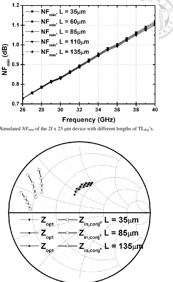
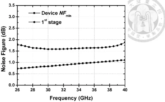
MSG/MAG and stability factor. Smaller total gate-periphery results in higher gain but lower stability. Device with the smallest gate-periphery of 2f x 25 μm has the highest MSG/MAG, but is potentially unstable, i.e., stability factor less than 1, at 38 GHz. Additional measures must therefore be adopted in order to stabilize the device if the 2f x 25 μm gate-periphery is to be used. Fig. 2.5 shows the simulated device NFmin from 26 to 40 GHz. The 2f x 25 μm and 4f x 25 μm devices have the lowest NFmin, with only small differences less than 0.1 dB from 26 to 40 GHz. Fig. 2.6 shows the input impedance for optimal noise matching (Zopt) from 30 to 40 GHz. At around 38 GHz, the Zopt of the 2f x 25 μm device is the closest to 50 Ω, which decreases the design difficulty and the impedance transformation ratio of the input matching network. A larger impedance transformation ratio requires longer transmission lines for matching, which lead to a larger insertion loss of the matching network. Insertion loss of the input matching network degrades both the gain and noise figure of the first stage, which are critical in LNA designs. Thus, considering all the performance comparisons mentioned above, the 2f x 25 μm device is selected for the proposed LNA design because of its well-suited performance and low DC power consumption.
Fig. 2.1. Simulated DC-IV curves of the device with gate periphery of 2f x 25 μm.
![Fig. 2.6. Simulated Z opt of the devices with different gate-periphery configurations at [V GS , V DS ]](https://thumb-ap.123doks.com/thumbv2/9libinfo/9603764.630071/43.892.85.813.112.1131/fig-simulated-opt-devices-different-gate-periphery-configurations.webp)