國立臺灣大學電機資訊學院電子工程學研究所 碩士論文
Graduate Institute of Electronics Engineering College of Electrical Engineering & Computer Science
National Taiwan University Master Thesis
應用於穿戴式裝置之 極低電壓無線收發機
Ultra-low-voltage Wireless Transceiver for Wearable Applications
王則惟 Tse-Wei Wang
指導教授:林宗賢 博士 Advisor: Tsung-Hsien Lin, Ph.D.
中華民國一百零五年七月 July, 2016
ii
iv
To My Dear Family
謹獻給我的家人
vi
謝辭
碩士生涯即將告一段落,這三年來的點點滴滴難以一言道盡。從換實驗室到 參加研究生協會以及小海豚舞蹈社,還有在碩士遇到了重要的人,即便最後無法 畫上完美的句點,但內心卻是充滿對各位的感謝。
首先必須感謝父母對我的支持以及關心,在碩士生涯的途中曾遇過無數次的 挫折,多虧了家人們的鼓舞以及建議才讓我能夠度過難關。
再來要感謝我的指導教授林宗賢博士這些年來的照顧,接納我這位原本不屬 於這間實驗室的研究生,同時對於我們的課外活動也樂觀其成。在電路設計上時 有突破性的觀點讓我受益良多,而且能夠容忍我時常犯的小錯誤,也給予了我許 多的機會表現,讓我的碩士生涯充實有內涵。
感謝我的口試委員曾英哲博士、黃柏鈞教授、陳信樹教授對於論文呈現的提 點,使我可以從別的角度審視自己的作品,彌補了許多曾被我遺漏的觀念細節。
感謝電二實驗室的各位成員,能與你們一同參與研究以及大大小小的活動是 我的榮幸。感謝畢業學長蔡宜霖、王邦全、陳建佑、林君豫、邱俊元奠定了實驗 室無線通訊電路的基礎,為我的低電壓無線傳輸電路題目解決了許多困難。感謝 已畢業學長翁展翔的指導,雖然研究領域與我大相逕庭,但報告時的電路觀點時 常令我收穫良多。謝謝邱茂菱學長幫忙處理實驗室網路的問題,我雖身為實驗室 的網管卻能力不足,多虧了學長的幫助才能夠度過難關。凃智展學長時有的電路 分析觀念總是能夠激發我更深層的思考,謝謝學長時常的教誨。感謝陳姿穎學姐 平日的人生觀解析,我雖然不常跟妳聊天但是很多觀念我都認同只是我沒說出來 而已。
感謝 100 級的學長姐對我的熱心關懷。還記得剛進實驗室時人生地不熟,多 虧了陳奕竹學長一開始的熱情招呼,還有魏子安學長一直很想借我錢幫忙我。劉 映辰學姐是清大時我就有耳聞的人物,原本以為會有距離感,但進來實驗室後發
現出乎我意料地活潑,也幫了我許多忙,萬分感謝。雖然在實驗室不常看到徐健 倫學長,但是覺得學長是冷面笑匠,可惜沒有能夠更進一步的認識。再來是感謝 何明諺學長一同跟我去國家晶片研究中心審查,第一次去面審的我也因為有學長 所以比較沒那麼害怕。最後當然是要謝謝周帝吉學長跟我一同畢業,因為有您的 存在讓我碩士生涯的最後一段路不會寂寞。
感謝 101 級的學長姐對我的照顧。同時身兼網管以及雲端的曾意婷學姐實在 太過強大,幫了我好多忙,可惜我連您的十分之一的戰力都沒繼承到,連兆軒科 技的電話都忘記了。如果沒有葉姿妤學姐在國科會計畫上的幫助,我無法想像我 的碩士生涯會因為這計畫過得多痛苦,也因為有您的無私奉獻,讓我理解到回饋 實驗室學弟妹的重要性。盛允楨學長的口頭禪-不行了、不行了真的是太好笑,雖 然說平時不講話看起來有些嚴肅,但是跟人交談的內容都很好笑,研究實力也有 目共睹,然後不行了這句口頭禪我已經傳下去了,別擔心會失傳。李峯文學長是 我在實驗室第一個看到的地縛靈,很難想像怎麼可以天天都那麼早來實驗室,然 後會做研究又很會打籃球真的是很厲害。何冠霖學長在最後的研究戰力大爆發令 我印象深刻,超強的每天行程就是一直用溫度箱量測、量測、量測。
感謝同屆伙伴們的陪伴,生活規律的陳冠中、我的大學同學-吳政輝、地縛靈 二號黃偉翔、效率一哥呂季桓。雖然我們這屆的畢業時間幾乎不一致,彼此在實 驗室的重疊時間也少,不過在我遇到困難需要解決的時候,你們往往有意無意間 幫了我很多忙,謝謝了。
103 級的學弟們珍重再見,能夠看著你們成長是身為學長我的福氣,尤其是 洪福聯學弟的轉變更是令人驚訝,只是口頭禪永遠都那幾個:啊我就是那麼廢啊!
死定了老師又要找我了!每天做報告就飽了啊!又怪我了!一開始遇見你們的時 候還覺得你們這屆很沉悶孤僻,應該是邊緣人,沒想到一個個都是神藏不露。有 很會煮咖啡的王鈺凱學弟,還有打 LOL 會轉性的林奕辰學弟,以及很少在實驗室 出現然後桌子很亂的李季安學弟。各位學弟加油,實驗室位子快要不夠坐了,趕 快在今年好好打包把位子讓出來吧。
viii
一群神經病之 104 級的學弟,我在實驗室好歹也有一段時間,但是從來沒看 過個性如此鮮明的一屆。陳友康是最奇特的一個,雖然電路實力很強,但真的是 很白爛。王敦儒真是有夠天才,不管學什麼都有夠快,但是平常不講話看起來有 距離感就是了。邱琛育學弟看起來很沒自信,可是身體卻出乎意外地壯,加油要 有自信一點!時常去健身的林聖穎學弟待人很和善,說話也滿有禮貌的,雖然會 抨擊我看美女圖,但念在是有事實的基礎上就不跟你計較了。很常被霸凌也很沒 自信的就是林登凱學弟,你也要加油,不要臣服於友康的惡勢力底下。還有就是 從別的實驗室轉來外表看起來很天兵,腦子更天兵會把自己反鎖在浴室的陳翰群 學弟,話說我覺得學弟你應該很受女生們的歡迎,要好好把握這個優勢。最後就 是承接我計劃的李忠容學弟,辛苦你了,學長我能夠留給你的東西不多,只能夠 靠平常嘴泡來舒緩你的壓力,你要加油,實驗室無線通訊電路的未來在你身上。
不好意思 105 級的學弟妹們雖然我都看過,但名字卻還沒辦法完全記起來,
所以我就不一個個點名了。我想對你們說的是,當年我大四的時候,你們才是剛 進大學的新鮮人。如今你們已經大學畢業準備念碩一,但你們絕對見不到碩四的 我。我真的很爽你們知道嗎?沒有啦!我開玩笑的,我只是想表達時間過得很快,
你們要好好把握時間,好好享受接下來的碩士生涯吧。
研究生協會是我碩一參加的社團,會進入這個社團是受到戴瑋珊會長的引領,
很開心可以遇到大家。曾友嶸學長十分多采多藝,而且在社會議題上的堅持令我 佩服。程巾芳學姐唱歌很好聽,陳力葦同學跟我一樣大學都是外校,所以莫名的 有話題,還有跟我同屆的盧潔人很和善笑笑地很好聊,祝妳未來研究順利。
最後的段落當然是要獻給最愛的小海豚舞蹈社。大學的時候我是空白人,從 來沒想過上研究所後能夠有機會跳到自己喜歡的舞蹈,更別提自己會變成社團那 麼重要的角色。礙於篇幅的關係,其實致謝只能夠打一頁但我現在已經超過了很 不好意思,所以就沒辦法把所有人都打出來,因為那可能有一百人以上。回正題,
我的大學課本現在有些在許凱傑學弟身上,曾經我是個課本不外借的人,不過現 在的我不太一樣,因為我覺得你滿有前途的,所以可以不用急著還我沒關係,我
相信那些書對你很有幫助。還有怪里怪氣的蔡丞昊學弟,莫名其妙變得很夯,不 過念在你很有上進心這部分我就原諒你,看著你也進步了很多,我心中也是無限 感慨,之後有空再一起練舞吧。再來是腹黑高欣妤學妹,外表看似清純善解人意,
但其實是演技一流,感謝妳某段時間一直聽我抱怨跟崩潰,要加油!看到自己喜 歡的對象的時候不要逃跑,真愛是值得追求的。我知道實驗室工作很忙,但也要 記得休息,沒錯就是在說妳彭郁茹學妹,妳已經瘦成人乾了,壓力再大真的會不 得了,要記得人生旅途上不是一昧地給自己壓力就算是成長喔。然後是身材一直 維持不變的吳駿杰,我是認真地建議要好好運動練身體,不只是為了把舞跳好,
也是為了身體的健康。還有在女生堆裡好像很吃香的洪詠翔學弟,但是好像有點 毛手毛腳,可以的話請克制一下,不然有人會吃醋,這是善意的提醒喔,好啦我 開玩笑的,祝福你變老人之後也不要鬆懈練舞,要好好地聽音樂,你的很多舞蹈 動作如果真的有對到點是很不賴的。外表看似可愛無害但其實打人很痛的李家欣 學妹請記得要好好收斂自己的殺氣,要不然會把喜歡妳的男生都嚇跑的,然後我 也很感謝妳聽我訴苦,雖然妳那時整個人都笑到翻過去了,再來我覺得妳其實可 以不用那麼焦慮,要能夠適時放下一些事情,不用力求完美,更不用因為自己做 不到一些事情就否定自己,要相信自己是很棒的人!還有我的女兒張杏瑜學妹,
妳也要好好地努力面對自己,但是切記別鑽牛角尖,要懂得接納自己的一切,唯 有如此,才能夠放開心胸,以便應付未來遇到的種種困難。最後是萌萌的徐嘉琪 學妹,感覺起來有點沒耐性有時講話會太直,但這看似是缺點的特性事實上也是 妳的優點。要加油之後別把自己搞得太忙,雖然我還是覺得妳仍然會莫名其妙答 應別人一堆事情就是了。然後感謝妳畢業舞會當天的陪伴,那是個令我難以忘懷 的美好回憶。
三年前的我從沒想到三年後的今天可以得到了這麼多的東西,如果可以,我 想再多打個十頁也不為過,真的是很謝謝各位了。
x
摘要
穿戴型裝置近年來已經成為全球業界與消費者熱烈關切的議題。為了達到長 時間操作的目的,低功率消耗將會是電路設計上最主要的考量之一。對於負責處 理傳送/接收訊號的無線收發機來說,更會是設計上的一大挑戰。
本論文提出了一個具有高能量效率,操作在 0.5V 供應電壓環境下,使用注入 式鎖定技巧之低功耗高效能無線收發機,調變方面採用差動式二元相位偏移 (D-BPSK)。
接收機部分主要是利用注入式鎖定的技巧,當接收之輸入訊號相位產生變化 時,震盪器的輸出振幅會產生暫時性的改變,即相位變化將透過注入式鎖定技巧 轉換為震盪器的振幅變化來完成解調。此架構不需閉迴路系統來完成相位同步,
可大幅簡化系統架構,進而降低功率消耗。本作品使用台積電 0.18 微米製程,系 統功耗為 0.97 毫瓦,靈敏度為-45dBm,最大資料傳輸量為 10 Mbps,在此資料 傳輸量下能量效率為 97 pJ/b。
發送機部分也是利用注入式鎖定技巧,低頻相位資訊會經由相位選擇器選取 後注入高頻振盪器,當低頻的相位發生改變,高頻振盪器便會重新鎖定並且改變 相位來完成調變。此架構因為不需產生高頻多相位的振盪訊號,因此可有效降低 整體功率消耗。本作品使用台積電 0.18 微米製程之模型來進行模擬,整體系統功 耗為 0.297 毫瓦,最大輸出功率為-9.7dBm,能量效率為 29.7 pJ/b,最大資料傳輸 量為 10 Mbps,在此資料傳輸量下誤差向量幅度為 13%。
Abstract
Wearable devices have been popular issues in recent years. Low power consumption is an important design target for the purpose of long-time usability. It’s also an enormous challenge for wireless transceivers circuit design.
This thesis proposes an energy-efficient injection-locked transceiver which operates at 0.5V voltage supply. The D-BPSK modulation and demodulation are adopted for this system.
The proposed receiver adopts injection-locked technique to demodulate received data. The injection-locked oscillator detects the input phase information and reacts on its output amplitude. In this receiver, the closed loop topology is not required for phase synchronization, which simplifies receiver design and reduce power consumption. This work is fabricated in TSMC 0.18-μm CMOS technology. The total power consumption is 0.97 mW with the sensitivity is -45 dBm at 10-Mbps data rate. The equivalent energy efficiency is 97 pJ/b.
The injection-locked technique is adopted in the transmitter design to modulate date. The injection locked oscillator will re-lock to a new phase when the phase changes at low frequency carrier. High frequency multi-phase oscillator is not required in this architecture; therefore it will reduce total power consumption significantly. This work is simulated under TSMC 0.18-μm CMOS technology. The total simulated power consumption is 0.297 mW with 13% EVM at 10-Mbps data rate. The maximum output power is -9.7 dBm, and the energy efficiency is 29.7 pJ/b.
xii
Table of Contents
List of Figures ... xv
List of Tables ... xix
Chapter 1 Introduction ... 1
1.1 Motivation ... 1
1.2 Data-rate Requirement ... 2
1.3 Operation Frequency Band ... 3
1.4 Modulation Scheme ... 3
1.5 Link Budget ... 6
1.6 Thesis Overview ... 7
Chapter 2 Introduction to Low-Power Wireless Transceiver ... 9
2.1 General Architecture of Wireless Transceiver ... 9
2.2 Low-Power Wireless Receiver ... 12
2.2.1 Super-Regenerative Receiver ... 12
2.2.2 Injection-Locked-Based Receiver ... 12
2.3 Low-Power Wireless Transmitter ... 15
2.3.1 OOK Transmitter ... 15
2.3.2 Phase-MUX-Based Transmitter ... 16
2.3.3 Injection-Locked Transmitter with Edge-Combining Technique ... 17
Chapter 3 Proposed Low-Power Injection-Locked D-BPSK Receiver ... 19
3.1 Receiver Introduction ... 19
3.1.1 Injection-Locked LC Oscillator Theory ... 19
3.1.2 Injection-Locked Oscillator as Phase-to-Amplitude Converter ... 22
3.2 System Architecture ... 24
3.2.1 The Proposed D-BPSK Receiver ... 24
3.2.2 Design Specfication of the Proposed Receiver ... 25
3.3 Circuit Implementation ... 27
3.3.1 Low Noise Amplifier and Multi-Stage Amplifier ... 27
3.3.2 Injection-Locked Dual-Conduction Digitally-Controlled Oscillator ... 30
3.3.3 Baseband Circuits ... 33
3.4 Simulation Results ... 33
3.5 Experimental Results ... 34
3.5.1 Die Photo ... 34
xiv
3.5.2 Measurement Environment Setup ... 35
3.5.3 PCB Design ... 36
3.5.4 Measured Results ... 37
Chapter 4 Proposed Low-Power Injection-Locked D-BPSK Transmitter ... 41
4.1 Transmitter Introduction ... 41
4.1.1 Motivation ... 41
4.1.2 Sub-harmonic Injection-Locked Oscillator as phase modulator ... 41
4.2 System Architecture ... 43
4.2.1 The Proposed D-BPSK Transmitter ... 43
4.2.2 Design Specfication of the Proposed Transmitter ... 44
4.3 Circuit Implementation ... 47
4.3.1 Pulse Generator ... 47
4.3.2 Sub-harmonic Injection-Locked Ring DCO ... 48
4.3.3 Power Amplifier ... 50
4.4 System Simulation Results ... 53
4.5 Experimental Results ... 53
4.5.1 Die Photo ... 53
4.5.2 Measurement Environment Setup ... 54
4.5.3 PCB Design ... 55
4.5.4 Measured Results ... 55
Chapter 5 Conclusions and Future Works ... 61
5.1 Conclusions ... 61
5.2 Future Works ... 61
References ... 63
List of Figures
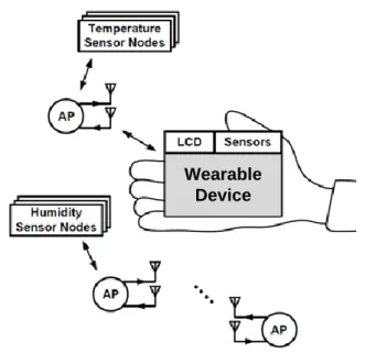
Fig. 1-1 Scenario of Wearable Mobile Device with Short-range Communication ... 1
Fig. 1-2 MedRadio Band from 401 MHz to 457 MHz ... 3
Fig. 1-3 BER versus Eb/No Graph ... 4
Fig. 1-4 Circuit implementation of (a) differential encoder (b) differential decoder ... 5
Fig. 2-1 Mixer-based Transmitter (a) Direct-conversion Transmitter [12] (b) Heterodyne Transmitter [13] ... 9
Fig. 2-2 PLL-based In-Loop-Modulation Transmitter ... 10
Fig. 2-3 Mixer-based Receiver (a) Direct-conversion Receiver [12] (b) Heterodyne Receiver [14] ... 11
Fig. 2-4 Super-Regenerative Receiver ... 12
Fig. 2-5 Injection-Locked BFSK Receiver ... 13
Fig. 2-6 Block diagram of the BPSK Demodulator/Receiver ... 14
Fig. 2-7 System Architecture of OOK Transmitter ... 15
Fig. 2-8 Injection-Locked OOK Transmitter [4] ... 16
Fig. 2-9 Phase-MUX-Based Transmitter ... 16
Fig. 2-10 Injection-Locked BFSK Transmitter with Edge-combining Technique ... 17
Fig. 2-11 Injection-Locked BPSK Transmitter with Edge-combining Technique ... 18
Fig. 3-1 Phasor diagram illustrating the phase difference between input signal and output signal in steady state ( is the steady state phase difference between Iosc and It) ... 19
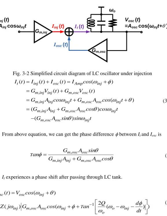
Fig. 3-2 Simplified circuit diagram of LC oscillator under injection ... 20
Fig. 3-3 Non-coherent DSPK detection using amplitude-to-phase conversion ... 22
xvi
Fig. 3-4 Simplified circuit of Injection-locked LC oscillator as phase-to-amplitude
converter ... 23
Fig. 3-5 Proposed DPSK Receiver with Phase-to-Amplitude Conversion ... 24
Fig. 3-6 Schematic of Low-Noise Amplifier ... 27
Fig. 3-7 Schematic of Multi-Stage Amplifier ... 28
Fig. 3-8 Simulated S11 of LNA ... 29
Fig. 3-9 Simulated overall voltage gain... 29
Fig. 3-10 Simulated overall noise figure ... 30
Fig. 3-11 Schematic of Dual-Conduction Digitally-Controlled Oscillator ... 31
Fig. 3-12 Simulated analog frequency tuning range of DCO ... 32
Fig. 3-13 Simulated phase noise of the DCO under different corners ... 32
Fig. 3-14 Simplified baseband circuit ... 33
Fig. 3-15 Time diagram of Proposed RX ... 34
Fig. 3-16 Die Photo of the Proposed RX ... 35
Fig. 3-17 Measurement Environment ... 35
Fig. 3-18 PCB for Testing ... 36
Fig. 3-19 Measured S11 Parameter ... 37
Fig. 3-20 Measured DCO Phase Noise ... 38
Fig. 3-21 Transient waveforms at 10-Mbps (Input power is -40 dBm) ... 38
Fig. 3-22 BER versus Input Power at 10-Mbps ... 39
Fig. 4-1 Phase-Noise Behavior of Injection-Locked VCO ... 42
Fig. 4-2 The diagram of phase modulation by sub-harmonic injection technique ... 43
Fig. 4-3 Proposed DPSK Transmitter with Sub-harmonic Injection-Locked Modulation… ... 44
Fig. 4-4 Pulse Generator ... 47
Fig. 4-5 The pulse width tuning range ... 48
Fig. 4-6 Single-ended Sub-harmonic Injection-Locked Ring Oscillator ... 49
Fig. 4-7 Simulated Phase Noise of Ring Oscillator (Carrier@430MHz) ... 49
Fig. 4-8 Class-E Power Amplifier and Output Impedance Transformation Network .... 51
Fig. 4-9 PA Output Spectrum ... 52
Fig. 4-10 Timing diagram of Proposed TX ... 53
Fig. 4-11 Die Photo of the Proposed TX ... 54
Fig. 4-12 Measurement Environments ... 54
Fig. 4-13 PCB for Testing ... 55
Fig. 4-14 TX Output Spectrum ... 56
Fig. 4-15 TX Output Power versus Frequency ... 56
Fig. 4-16 TX free-running transient waveform ... 57
Fig. 4-17 Measured TX Output Phase Noise ... 58
xviii
List of Tables
Table 1-1 Illustration of differential encoding and decoding of BPSK ... 6
Table 3-1 Designing Specifications of D-BPSK Receiver ... 26
Table 3-2 Simulated characteristics of LNA and AMP @ TT27 o ... 30
Table 3-3 Transistor size and operating point of the Gm stage under corner TT27o ... 31
Table 3-4 Simulated characteristics of the DCO @ TT27 o ... 32
Table 3-5 Power Breakdown of the D-BPSK RX ... 39
Table 3-6 Comparison Table of the Proposed RX ... 40
Table 4-1 Designing Specifications of D-BPSK Transmitter ... 47
Table 4-2 Simulated characteristics of the DCO @ TT27 o ... 50
Table 4-3 Simulated characteristics of the PA @ TT27 o ... 52
Table 4-4 Power Breakdown of the D-BPSK TX ... 58
Table 4-5 Comparison Table of the Proposed TX ... 59
1.1 Motivation
Chapter 1 Introduction
1.1 Motivation
As the information and communication technology improve, the connection between people and the world become more flourishing than before. In consideration of security and health, the traditional devices such as cell phone with camera and long-distance transmission are forbidden in many places. Therefore, the IoT applications with short-distance communication are required in many fields. Fig. 1-1 shows the scenario of wearable mobile media for IoT application. This application composes of several biomedical sensor nodes to capture biomedical data and transmits it to nearby AP node by short-range wireless transmitter. A short-range wireless receiver is also required for wearable device to obtain information outside from AP node.
Wearable Device
Fig. 1-1 Scenario of Wearable Mobile Device with Short-range Communication
Chapter 1 Introduction
2
Since the wearable device is a mobile product, the long-time usability are significant important. In wireless wearable device, the power source for the whole system is energy harvesting circuits. Therefore, low power consumption is one of the major design concerns in the system. To integrate the whole system in low voltage is needed. On the other hand, the wearable device transmits and receives information though only several meters distance, so the specification of output power for transmitter and sensitivity for receiver are much relaxed.
1.2 Data-rate Requirement
The sufficient data rate is required for the transceiver. In consideration of transmitter, it’s required to transmit biomedical information to AP node. As expressed in (1-1), data rate not only depends on the number of recording sensor (Nsensor) in wearable device, but also relies on the resolution of ADC (Nbit), and the sampling rate of ADC (fsampling). Take an 1-lead electrocardiography (ECG) recording system which is integrated in wearable device node for example, and assume that a 10-bit ADC with 10-kHz sampling frequency is adopted. The uncompressed data rate will be 1×10k×
10=100 kbps. Nevertheless, if the transmitter is designed for more complex bio-signal recording such as 128-channel electroencephalography (EEG) monitoring, the required data rate could be up to 12.8 Mbps [1].
In view of several sensors in AP nodes, the wearable device node must receive huge information. In other word, the receiver in wearable device also requires high data rate specification as that of transmitter.
sensor sampling bit
Data rate N f N (1-1)
1.3 Operation Frequency Band
1.3 Operation Frequency Band
Federal communications commission (FCC) established the Medical Implant Communication Service (MICS) and set aside 401 – 406 MHz spectrum. However either 100-kHz or 300-kHz channels is not sufficient for much sophisticate applications.
Therefore FFC combined the 413-MHz to 457-MHz MHz band with the previous MICS band as the new Medical device Radio-communications Service (MedRadio) spectrum in 2011 [2]. The illustration of the spectrum allocation is shown in Fig. 1-2.
438 444 451 457 426 432
413 419 406
… … 401 MHz
10x300k-Hz Channels
……
402 405
10x100k-Hz Channels 10x100k-Hz
Channels
6 MHz
-20 dB
MedRadio Band MICS Band
Fig. 1-2 MedRadio Band from 401 MHz to 457 MHz
MedRadio band is suitable for wearable application because of sufficient and the license is not required. Several symmetric transceivers aiming at MedRadio band have been published [1][3], achieving low-power performance but not operating efficiently.
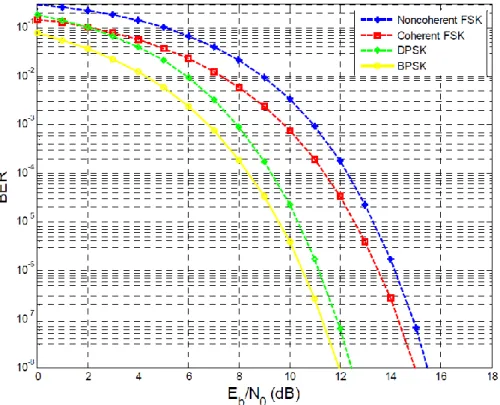
1.4 Modulation Scheme
On-off keying (OOK) modulation is the special case of amplitude-shift keying (ASK), which is widely chosen for low-power systems due to the simplicity of circuit implementation [4]-[8]. Nevertheless, OOK modulation is susceptible to interference and the bandwidth efficiency is poor than that of phase-shift keying (PSK) or frequency shift keying (FSK). Therefore OOK is not suitable for wearable application due to its poor noise performance than that of FSK/PSK. Fig. 1-3 depicts the
Chapter 1 Introduction
4
theoretical noise performance of the coherent FSK, non-coherent FSK, binary phase-shift keying (BPSK) and differential phase-shift keying (DPSK). Overall, the noise performance of PSK is superior to that of FSK. Hence it is easier to achieve energy-efficient transceiver with better sensitivity of receiver by implementing PSK modulation.
Fig. 1-3 BER versus Eb/No Graph
In low-power systems, the non-coherent demodulation such as DPSK demodulation is desirable because the phase-tracking loop is no longer needed for phase synchronization, which reduces power consumption [9]. Although the required SNR for demodulating non-coherent PSK carrier is higher than that of synchronized PSK demodulation, DPSK is an acceptable modulation based on simplified circuit architecture for low power specification.
1.4 Modulation Scheme
Differential phase shift keying such as D-BPSK is to deliver data by adding a relative phase change to the carrier signal rather than encode absolute phase for each baseband data. As shown in (1-2) and (1-3), extra 180° phase may be added to the current phase for transmitting a binary ‘1’, and no extra phase change in carrier when transmitting a binary ‘0’.
0 2 ,
, ) 2 cos(
0 , ) 2 ) cos(
0( for binary
T t T t f A
T t t
f t A
s
C C
(1-2)
1 2 ,
, ) 2
cos(
0 , ) 2 ) cos(
1( for binary
T t T t
f A
T t t
f t A
s
C C
(1-3)
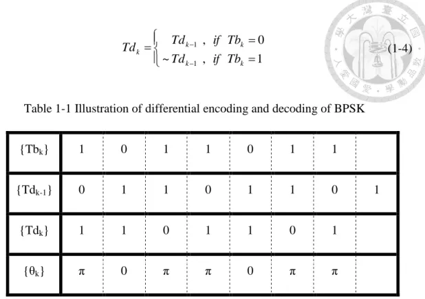
In other word, the absolute phase information is no longer important compared with traditional phase modulation, which relaxes the circuit design requirement for transceiver. The implementation of differential encoder and decoder of D-BPSK is shown in Fig. 1-4.
D Q {Tbk} {Tdk}
{Tdk-1}
CLK
{Rdk} {Rbk}
D Q {Rdk-1} CLK
(a) (b)
Fig. 1-4 Circuit implementation of (a) differential encoder (b) differential decoder The differential encoding scheme is shown in Table 1-1. {Tbk} denotes the original data sequence for transmitting, {Tdk} represents the encoded data sequence, and {θk} stands for the phase change of {Tdk}. The definition of {Tdk}is in (1-4).
Chapter 1 Introduction
6
1 ,
~
0 ,
1 1
k k
k k
k Td if Tb
Tb if
Td Td (1-4)
Table 1-1 Illustration of differential encoding and decoding of BPSK
{Tbk} 1 0 1 1 0 1 1
{Tdk-1} 0 1 1 0 1 1 0 1
{Tdk} 1 1 0 1 1 0 1
{θk} π 0 π π 0 π π
1.5 Link Budget
The RF link budget has to be estimated in order to decide the specification of TRX front-end circuit [9]. The path loss due to signal propagation can be estimated by free-space loss equation shown in (1-5).
20log 4
path
L d
(1-5)
is the wave-length, and d is the distance between the wearable device and AP node. If the operating frequency is 400 MHz and the distance is 5 meters, the path loss is about 38 dB.
recieved out antenna path
P P G L (1-6)
In (1-6), Pout is the TX output power, and Gantenna is the antenna gain of TX/RX.
To meet the standard of Med-radio band, the TX output power is -10 dBm. Assume a
1.6 Thesis Overview
chip antenna with -10-dBi antenna gain is adopted; as a result, for 5-meter distance, the received power is about -58dBm.
From the above calculation, the RX sensitivity, which is defined as detectable signal power for a certain BER of demodulated data [10][11] is -60 dBm.
1.6 Thesis Overview
This thesis presents the design of low voltage D-BPSK transceiver, including theoretical analysis, simulated and measured results.
Chapter 2 introduces the state-of-the-art low-power transceivers for WBAN applications, which covers traditional wireless transceivers and injection-locked-based transceivers.
Chapter 3 presents the proposed ultra-low-voltage D-BPSK receiver based on injection-locked technique, which includes the dynamic phase-to-amplitude conversion analysis.
Chapter 4 describes the proposed ultra-low-voltage D-BPSK transmitter. The theory of sub-harmonic injection-locked phase modulation for low-power consideration is also presented.
Finally, chapter 5 provides a conclusion and the future work.
2.1 General Architecture of Wireless Transceiver
Chapter 2 Introduction to Low-Power Wireless Transceiver
2.1 General Architecture of Wireless Transceiver
Mixer-based transmitters are widely applied in many wireless systems [12]-[14].
As shown in Fig. 2-1, there are two common mixer-based architectures. The direct-conversion transmitter uses digital-to-analog converter (DAC) and mixers for transforming baseband data to analog format and performing up-conversion task.
However, this topology suffers from injection pulling effect between power amplifier and carrier, so another type which adopts heterodyne topology for separating carrier frequency from the PA output spectrum by making the signal up-conversion in two steps had become popular. Nonetheless, these two topologies must deal with the trade-off between maximum data rate which is limited by the bandwidth of DAC and power consumption. Therefore, mixer-based transmitters are not appropriate choices for low-power applications.
DAC
Digital CLKBB Mod.
DAC
cos(ωct)
sin(ωct) Carrier Gen.
IBB
QBB
PA
TXOUT LPF
LPF
(a)
Chapter 2 Introduction to Low-Power Wireless Transceiver
10 DAC
Digital CLKBB Mod.
DAC
cos(ωct) sin(ωct)
Carrier Gen.
IBB
QBB
PA
TXOUT
LPF
LPF cos(Nωct)
cos(ωct) ÷N sin(ωct)
(b)
Fig. 2-1 Mixer-based Transmitter (a) Direct-conversion Transmitter [12] (b) Heterodyne Transmitter [13]
The PLL-based in-loop-modulation transmitter [15] is another common transmitter architecture. As depicted in Fig. 2-2, the digital data which is encoded by the digital baseband modulates the frequency divider to accomplish FSK modulation.
This modulation requires phase-locked loop (PLL), which results in much higher power consumption. In addition, the limited data rate is the primary disadvantage due to the bandwidth of PLL. To sum up, the PLL-based topology is more suitable for narrow-band applications rather than high-energy-efficient ones.
Digital CLKBB Mod.
TXOUT
LPF PFD/CP
CLKREF
PA
DIV
Fig. 2-2 PLL-based In-Loop-Modulation Transmitter
2.1 General Architecture of Wireless Transceiver
The direct-conversion receiver and heterodyne receiver shown in Fig. 2-3 play important parts in wireless communication. The former one solves the out-band interference problem and save intermediate frequency (IF) filter, but the carrier operating at higher frequency is needed in this receiver, which tightens total power budget. The latter one provides the two-step down-conversion facilitate. However, the non-zero IF down-conversion causes the image problem. Although these architectures are commonly used for different specification, power-hungry circuits such as ADCs and mixers are needed, which is the limitation for low-power system.
Digital BB.
cos(ωct)
sin(ωct)
Carrier Gen.
IBB
QBB
RFIN
LPF
LPF LNA
VGA
VGA ADC
ADC
(a)
Digital BB.
cos(ωct) sin(ωct)
Carrier Gen.
IBB
QBB
RFIN
LPF
LPF LNA
VGA
VGA ADC
cos(Nωct) ADC
÷N cos(ωct) sin(ωct)
(b)
Fig. 2-3 Mixer-based Receiver (a) Direct-conversion Receiver [12] (b) Heterodyne Receiver [14]
Chapter 2 Introduction to Low-Power Wireless Transceiver
12
2.2 Low-Power Wireless Receiver
2.2.1 Super-Regenerative Receiver (SR RX)
The signal-regeneration characteristic of super-regenerative receiver (SR RX) is suitable for demodulating OOK and FSK signal while consumes little power [7][16][17]. Fig. 2-4 shows the basic operation of SR RX. The RF carrier which is amplified by LNA injects to a periodically quenched oscillator. Then, the envelope detector (ED) detects input-dependent envelope of oscillator whose output pulse width contains the data information.
The periodically quenched oscillator operate with heavy duty-cycled and RX only requires simple mechanism to demodulate data, which makes SR RX be a famous solution for low-power application. However, the worse frequency selectivity and the requirement of high-Q passive components limit the development of the SR RX.
RFIN Envelope
Detector
LNA VED
Quench Controller
Fig. 2-4 Super-Regenerative Receiver 2.2.2 Injection-Locked-Based Receiver
Injection-locking phenomenon in an oscillator is commonly used for providing frequency division or LO generation. Moreover, the low-power receivers based on the
2.2 Low-Power Wireless Receiver
injection-locked technique develops rapidly in recent years. Fig. 2-5 shows the block diagram and operation mechanism of the injection-locked BFSK receiver architecture [18]. The key point of the FSK demodulation capability is the frequency selectivity of the ILO. The ILO acts as a band-pass filter and it transforms frequency difference between RF data into amplitude difference. The envelope detector captures and recovers input-dependent amplitude information. The major drawback is the small amplitude difference (~2mV) converted from frequency difference, which implies wider frequency deviation, hence more bandwidth is needed. Therefore, injection-locked based FSK receiver suffers from poor bandwidth-efficient performance.
Frequency
Amplitude
ωinj,1
ωinj,2
DA Dω
Envelope Detector
LNA VED
FSKData
ILO
Fig. 2-5 Injection-Locked BFSK Receiver
The synchronization between receiver and transmitter is needed for PSK demodulation in traditional receiver. Non-linear BPSK demodulation schemes using injection-locking technique were proposed [19][20] recently, which consists of two super-harmonic injection-locked oscillators (SH-ILO) and an XOR gate as shown in Fig.
2-6. The principle of non-linear BPSK demodulator depends on the dynamics of two super-harmonic injection-locked oscillators. The BPSK modulated signal is injected to the two oscillators, which makes one of the oscillators obtain a phase lead, the other
Chapter 2 Introduction to Low-Power Wireless Transceiver
14
obtain a phase lag. Then an XOR operation combines the oscillator output. The circuit is well-suited to achieve low-power consumption as a result of simplified architecture and the oscillator running at one-half the input signal frequency.
When a BPSK modulated input signal is fed to the 2nd harmonic injection-locked oscillators, its output frequency is one-half of input frequency. If the oscillator is locked with no phase change, the phases of two injection-locked oscillators are the same, which makes the output of XOR produce 0. On the other hand, an 180゜phase change of the BPSK modulated input signal leads to ±90゜output phase (D) change of the SH-ILOs as shown in (2-1).
1
2
90 , 2
90 , 2
inj
osc in
inj
osc in
D
(2-1)
180 o phase shift in the input signal results in 90 o phase lag at the output of ILO1 if
osc1 < in and 90 o phase lead at the output of ILO2 ifosc2 > in. In short word, a total phase difference is 180 o between ILO1 and ILO2, which makes output of XOR produce 1.
Frequency
Amplitude
ωin
ωosc1
Power
Divider ILO1 PSKData
XOR
ωosc2
ILO2
VBB
Fig. 2-6 Block diagram of the BPSK Demodulator/Receiver
2.3 Low-Power Wireless Transmitter
To prevent the pulling effect between two oscillators, the frequency separation between ILOs must be far enough, so that the required gain of RF front-end circuit must increase for larger injection power. Therefore, this type of receiver needs excess power for RF front-end circuit due to gain requirement. Furthermore, a tradeoff between frequency difference and data rate is significant. The pulling effect becomes severe if frequency difference decreases for data-rate requirement at fixed injection power. To sum up, this architecture is ill-suited to low-power applications at sub-GHz range.
2.3 Low-Power Wireless Transmitter
2.3.1 OOK Transmitter
The OOK transmitters are widely adopted in many low power systems [4]-[8].
The traditional implementation is to switch PA or carrier directly, which simplifies circuit architecture and relaxes system power budget. An injection-locked OOK transmitter was published to achieve higher energy efficiency, as briefly depicted in Fig. 2-8. However, the innate limit such as insufficient bandwidth efficiency burdens the usability of OOK transmitter for low-power and high-data-rate applications.
Digital CLKBB Mod.
PA TXOUT
Carrier
CLKREF Gen. CLKREF
Digital CLKBB Mod.
PA TXOUT
Carrier Gen.
Fig. 2-7 System Architecture of OOK Transmitter
Chapter 2 Introduction to Low-Power Wireless Transceiver
16 Ref OSC Power Osc
Digital CLKBB Mod.
TXOUT ωOSC
Fig. 2-8 Injection-Locked OOK Transmitter [4]
2.3.2 Phase-MUX-Based Transmitter
Phase-multiplexing (Phase-MUX) technique is greatly preferred in low-power PSK transmitter design recently [1]. The frequency carrier produces multi-phase information and is followed by a multiplexer. The encoded digital control signal modulates the multiplexer to switch the phase of carrier for accomplishing PSK modulation. This technique relaxes the trade-off between power and bandwidth, eliminating the power-hungry block such as mixer, LPF, and DAC. Nevertheless, the multi-phase carrier generators which operate at high frequency become the most power-hungry block in transmitter. Therefore, Phase-MUX based transmitter is an improper alternative for ultra-low-power applications.
Digital TXDATA Mod.
PA TXOUT
Multi-phase Generator CLKREF
MUX
Fig. 2-9 Phase-MUX-Based Transmitter
2.3 Low-Power Wireless Transmitter
2.3.3 Injection-Locked Transmitter with Edge-Combining Technique
Injection-locked transmitter with edge-combining technique has been proposed to low-power FSK/PSK transmitters [7][21][22]. The injection-locked transmitter behaves as a first-order PLL, which the free-run frequency of oscillator could be locked to the nth harmonic of the injection reference frequency [23]. Without any extra power-hungry part such as high-frequency divider, phase frequency detector (PFD), and charge pump (CP), so injection-locked oscillator (ILO) is energy-efficient circuit block to reduce power consumption.
Fig. 2-10 shows the system architecture of a low-power BFSK injection-locked transmitter for MICS/ISM band [21]. This transmitter achieves low-power performance through edge-combing technique. The edge combiner (EC) mixes low-frequency multi-phase signal to generate signals at RF frequency. Therefore, the power consumption is much less than the one of Phase-MUX based transmitter because most circuit block including multi-phase carrier operate at low frequency.
Although this transmitter relaxes power budget, the FSK modulation suffer from poor spectrum efficiency comparing with that of PSK modulation.
FSK data
ILRO2
High Frequency Low
Frequency
…
EC/PA
TXOUT ILRO1
…
Fig. 2-10 Injection-Locked BFSK Transmitter with Edge-combining Technique
Chapter 2 Introduction to Low-Power Wireless Transceiver
18
In [22], a low-power BPSK injection-locked transmitter was presented for both low-power and excellent spectrum efficiency performance. It merges the advantage of phase multiplexer and edge-combining techniques as shown in Fig. 2-11. However there’re several issues in this design. First, the number of combining path depends on the ratio between injected frequency and RF frequency. Even in simple phase modulation such as BPSK, it will require multi-path circuit due to the frequency difference between injected signal and RF carrier, which complicates the design.
Furthermore, the spurs due to the phase mismatch of edge combiner will degrade spectrum performance. The phase calibration technique is needed to address this issue.
CLKINJ
Pulse
Gen. 9-stage
Ring VCO
…
EC/PA
…
MUX … TXOUT
Digital TXDATA Mod.
Fig. 2-11 Injection-Locked BPSK Transmitter with Edge-combining Technique
3.1 Receiver Introduction
Chapter 3 Proposed Low-Power Injection-Locked D-BPSK Receiver
3.1 Receiver Introduction
3.1.1 Injection-Locked LC Oscillator Theory
Injection-locked LC oscillator is commonly used for many low-power receivers [18]-[20]. The related theories about LC oscillator under injection were published in [24][25].
An injection-locking or pulling phenomenon occurs when a periodic signal feeds to an oscillator. If injection-locked frequency inj is close to the free-running frequency
o, the output frequency will be locked to inj and the current output It will be combined with input current Iinj and free-running current Iosc as shown in Fig 3-1.
Iosc Iinj
2 -π
2 π
It
0
Fig. 3-1 Phasor diagram illustrating the phase difference between input signal and output signal in steady state ( is the steady state phase difference between Iosc and It)
Chapter 3 Proposed Low-Power Injection-Locked D-BPSK Receiver
20
The conceptual block diagram of an LC oscillator under injection is shown in Fig.
3-2, where the incoming voltage-domain signal (Vinj) is first converted to current domain signal (Iinj) by a transconductance stage, and then added with oscillator current (Iosc). The resultant current (It) is injected to a resonator whose central frequency is o
and converted back to voltage (Vosc) domain. The equations describing the injection- locking phenomenon under these conditions are derived in (3-1)-(3-9).
Vinj (t)
=Ainj cosωinjt
Gm,inj
Gm,osc
Vosc (t)
=Aosc cos(ωinjt+ ) ωo
Iinj (t)
Iosc (t)
It (t)
Fig. 3-2 Simplified circuit diagram of LC oscillator under injection
, ,
, ,
, ,
,
( ) ( ) ( ) ( )
( ) ( ) ( )
( ) (
( )
) ( )
( )
( )
t inj osc Amp inj
m inj inj m osc osc
m inj inj inj m osc osc inj
m inj inj m osc osc inj
t t
m osc osc inj
t t
I t I t I t I cos
G V t G V t
G A cos t G A cos t
G A G A c
I t I t I t I t
os cos t
G A sin sin t
(3-1)
From above equation, we can get the phase difference between It and Iosc is
,
, ,
m osc osc m inj inj m osc osc
T G A sin
an G A G A cos
(3-2)
It experiences a phase shift after passing through LC tank.
1 ,
( ) ( )
( ) ( 2 ( ) )
osc osc inj
inj m osc osc inj o inj
o T
V t V cos
Q d
Z j G A cos an
dt
(3-3)
3.1 Receiver Introduction
From (3-3), we observe the relationship between phase and phase with that
1 2
( o inj )
o
T Q d
an dt
(3-4)
The change rate of phase is close to that of phase .
d d
dt dt
(3-5)
Furthermore
,
, ,
, ,
( )
1
m inj inj
m osc osc m inj inj m inj inj inj
m osc osc osc
T G A sin Ksin
an G A G A cos Kcos
G A I
K G A I
(3-6)
Under locked condition, the phase difference remain constant with time can derive the relationship between locking range L and injection current ratio K from (3-4), (3-5), and (3-6).
( ) ( )
2 2 1 0
o
o inj
o inj o
d t T
dt Q an
Ksin Q Kcos
(3-7)
Locking range is the difference between free-running frequency and injection frequency which can be computed as shown in (3-8).
2 1
o inj o
Ksin
Q Kcos
(3-8)
The maximum locking range can be calculated by substituting [25], and we final get
Chapter 3 Proposed Low-Power Injection-Locked D-BPSK Receiver
22 2 1 2 L o injmax o
K
Q K
(3-9)
3.1.2 Injection-Locked Oscillator as Phase-to-Amplitude Converter
Envelope detection is widely applied in the non-coherent AM demodulation for its simplicity. The phase-to-amplitude conversion can be applied in order to demodulate the D-BPSK signal. Fig. 3-3 illustrates the operation of phase-to-amplitude conversion.
Envelope Detector
VED(t)
VD-BPSK(t) VSUM(t)
Delay Tb
VD-BPSK(t-Tb)
Fig. 3-3 Non-coherent DPSK detection using amplitude-to-phase conversion This phase-to-amplitude conversion demodulates data by comparing the phase difference between received signal VDPSK(t) and former received signal VDPSK(t-Tb), where Tb is one-bit period.
Assume VDPSK(t) and VDPSK(t-Tb) are in-phase in initial status, the amplitude of VSUM(t) will increase due to the summation. On the other hand, the amplitude of VSUM(t) reduces due to the summation of two anti-phase signals VDPSK(t), VDPSK(t-Tb). Then the phase-to-amplitude information will be captured by envelope detector. Moreover, this method is not a proper choice for receiver at RF frequency, because an exact delay element is difficult to be accomplished without dramatically increasing power consumption.
3.1 Receiver Introduction
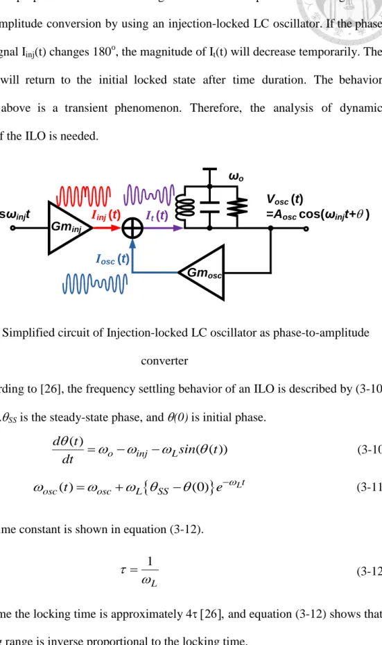
Instead a phase-to-amplitude conversion technique by using injection-locked oscillator is proposed in this work. Fig. 3-4 is a conceptual block diagram of phase-to-amplitude conversion by using an injection-locked LC oscillator. If the phase of input signal Iinj(t) changes 180o, the magnitude of It(t) will decrease temporarily. The oscillator will return to the initial locked state after time duration. The behavior described above is a transient phenomenon. Therefore, the analysis of dynamic behavior of the ILO is needed.
Vinj (t)
=Ainj cosωinjt
Gminj
Gmosc
Vosc (t)
=Aosc cos(ωinjt+ ) ωo
Iinj (t)
Iosc (t)
It (t)
Fig. 3-4 Simplified circuit of Injection-locked LC oscillator as phase-to-amplitude converter
According to [26], the frequency settling behavior of an ILO is described by (3-10) and (3-11).SS is the steady-state phase, and (0) is initial phase.
( ) o inj L ( ( ))
d t
sin t dt
(3-10)
( ) (0) Lt
osc t osc L SS e
(3-11)
The time constant is shown in equation (3-12).
1
L
(3-12)
Assume the locking time is approximately 4 and equation (3-12) shows that the locking range is inverse proportional to the locking time.
Chapter 3 Proposed Low-Power Injection-Locked D-BPSK Receiver
24
The ILO converts relative phase information to amplitude variation depending on its transient behavior, that is to say, the ILO change state between the locked state and the state. Since the locking time is an important parameter on this receiver, and the detailed analysis such as relationship between locking time and circuit specification for receiver will be discussed in the following paragraphs.
3.2 System Architecture
3.2.1 The Proposed D-BPSK Receiver
The proposed architecture of the DPSK receiver, as shown in Fig. 3-5, is composed of a matching network, a low-noise amplifier (LNA), the multi-stage amplifier (Amp), a injection-locked oscillator (ILO), an envelope detector, and a data slicer.
LNA and the following multi-stage amplifier amplify the received D-BPSK signal (RFin). Before injecting to the ILO, the amplified signal is converted from voltage domain to current domain by a transconductance stage. Therefore, the ILO performs dynamic phase-to-amplitude conversion, then the envelope detector extracts the amplitude information, and the received signal is therefore down-converted to baseband.
Finally, data slicer recovers the analog signal to a digital output.
Matching
Network ILO
AMPout
RFIN
Envelope Detector
LNA AMP Data
Slicer ILOout EDout RXout
Fig. 3-5 Proposed DPSK Receiver with Phase-to-Amplitude Conversion
3.2 System Architecture
3.2.2 Design Specifications of the Proposed Receiver
The sensitivity of RX is defined as detectable signal power for certain BER of demodulated data [11].
(dBm) No 10log( ) min
Sensitivity B NFSNR (3-13)
N0 is thermal-noise power in 1-Hz noise bandwidth, B is equivalent noise bandwidth, NF is noise figure of RX front-end circuit, and SNRmin is the minimal SNR required for DPSK demodulation. According to BER-to-SNR graph shown in Fig. 1-3, the minimal SNR of DSPK demodulation for 10-3 (0.1 %) BER is around 7 dB.
Assume the sensitivity is equal to the received power calculated in Chapter 1.6, and the equivalent noise bandwidth is 10 MHz for high-data-rate application, we can determine the NF of front-end circuit is about 23 dB, which isn’t a tight specification for receiver.
Another critical requirement is the front-end gain which affects the specification of maximal data rate for receiver. As mentioned in Chapter 3.1.1, demodulation is based on the transient characteristic of the ILO, so the locking time (4) must be less than data-transmitted time for successful demodulation..
4 4
S b
L
T T
(3-14)
Chapter 1.2 determines the maximum data rate requirement is 10 Mbps, in other word, the bit interval is 100ns. According to (3-14), the locking range L of ILO must be larger than 2*6.366 MHz. Chapter 3.1.1 analyzes the relationship between locking range and injection power ratio K. Substituting the design parameter o=405 MHz and Q is 7.6 into (3-9), the required injection ratio K can be estimated, which is about 0.83.
Chapter 3 Proposed Low-Power Injection-Locked D-BPSK Receiver
26
The injection power ratio is determined by front-end gain ARF, oscillator current IOSC, and input signal Vin as depicted in (3-15).
inj in RF m inj,
osc osc
I V A G
K I I (3-15)
Vin=316 V (-60 dBm) which is equal to the sensitivity, and assume the transconductance Gm=2 mA/V, IOSC = 400 A, the requirement of front-end gain is 151 (43dB).
To sum up, due to the injection-locking characteristic of LC-tank oscillator for dynamic phase-to-amplitude conversion, the requirement of maximal data rate determines the locking range and the front-end gain. Above analysis provides insights into the design of RX system. The specification of this work is shown in Table3-1 in the end.
Table 3-1 Designing Specifications of D-BPSK Receiver
Process TSMC 0.18-m CMOS
Supply Voltage 0.5 V
Operating Frequency 414 ~ 457 MHz
Data Rate 10 Mbps
Sensitivity < -60 dBm
Modulation D-BPSK
Power Consumption < 0.5 mW Energy Efficiency < 50 pJ/b
![Fig. 2-1 Mixer-based Transmitter (a) Direct-conversion Transmitter [12] (b) Heterodyne Transmitter [13]](https://thumb-ap.123doks.com/thumbv2/9libinfo/9605510.631571/32.892.188.785.117.404/mixer-based-transmitter-direct-conversion-transmitter-heterodyne-transmitter.webp)