行政院國家科學委員會專題研究計畫 成果報告
新穎光電半導體材料,低維度微細結構及其元件構造之光學 特性研究(3/3)
計畫類別: 個別型計畫
計畫編號: NSC93-2215-E-011-001-
執行期間: 93 年 08 月 01 日至 94 年 10 月 31 日 執行單位: 國立臺灣科技大學電子工程系
計畫主持人: 黃鶯聲
計畫參與人員: 許宏彬、黃冠賓、吳秉諭、王季霖、高嘉維、黃文彥
報告類型: 完整報告
處理方式: 本計畫可公開查詢
中 華 民 國 94 年 8 月 3 日
行政院國家科學委員會補助專題研究計畫 ■ 成 果 報 告
□期中進度報告
新穎光電半導體材料,低維度微細結構及其元件構造 之光學特性研究(3/3)
Optical Properties Study of Novel Optoelectronic Semiconductor Materials, Low Dimensional Microstructures and Device Structures
計 畫 類 別 : ■ 個 別 型 計 畫 □ 整 合 型 計 畫 計 畫 編 號 : NSC 93 - 2215 - E - 011 - 001 執行期間: 93 年 8 月 1 日 至 94 年 10 月 31 日
計 畫 主 持 人 : 黃 鶯 聲
計畫參與人員:許宏彬、黃冠賓
國立台灣科技大學電子工程所博士班研究生 吳秉諭、王季霖、高嘉維、黃文彥
國立台灣科技大學電子工程所碩士班研究生
成果報告類型(依經費核定清單規定繳交):□精簡報告 ■完整報告
本成果報告包括以下應繳交之附件:
□赴國外出差或研習心得報告一份
□出席國際學術會議心得報告及發表之論文各一份
處理方式:除產學合作研究計畫、提升產業技術及人才培育研究計畫、列管計畫 及下列情形者外,得立即公開查詢
□涉及專利或其他智慧財產權,□一年□二年後可公開查詢
執行單位:國立台灣科技大學電子工程所
中 華 民 國 94 年 7 月 30 日
I
一、中文摘要
本計畫目的主要利用調制光譜及表面光電壓 量測技巧來研究 II-VI 族 ( 如 ZnCdBeSe 等)及 III-V 族(如 GaInNP、GaInNAs)半 導體化合物材料的光學特性。另外也利用 上 述 量 測 技 巧 來 量 測 面 射 型 雷 射 二 極 體 (VCSEL)元件特性。
在ZnCdBeSe 方面,CER 及 PzR 光譜可得到 因晶格常數不匹配所造成價電帶分裂之輕電 洞(light-hole, lh)及重電洞(heavy-hole, hh)躍 遷訊號, 藉 由 PzR 光 譜 可 將 lh 分 辨 出 來 。 另 外 在 GaInNP 部 份 , 主 要 使 用 PzR 光 譜 配 合 極 化 量 測 技 巧 來 判 定 材 料 之 非 對 稱 性 。 並 探 討 上 述 化 合 物 半 導 體 不同訊號隨溫度變化之情形。
在 GaInNAs 量子井中,我們利用 PL 及 PR 量測各個躍遷位置隨溫度變化的情形,並分 析其溫度係數。
我們也利用表面光電壓量測技巧來檢測面射 型雷射二極體的元件特性,並分析元件特性 隨溫度變化的情形。
關鍵詞:非接觸式電場調制、壓電調制、II- VI 族寬能隙半導體、氮、III-V 族四元化 合物、面射型雷設二極體。
Abstract
Using contactless electroreflectance and piezo- reflectance spectroscopy to characterize II-VI wide band gap material ZnCdNeSe and III-V N-related quaternary GaInNP films.
From CER and PzR spectra, we get both the lh and hh transition energy, and the PzR spectra can identify the lh signal.
We also observed the anisotropic properties utilize polarized piezoreflectance in GaInNP films. The
different transitions energy with temperature Variation are also evaluated and discussed. GaInNAs /GaAs single quantum well (SQW) structures have been characterized by photoreflectance (PR) and photoluminescence (PL). The temperature dependence analysis yields information on the parameters that describe the temperature variations of the interband transitions.The detailed study of
vertical cavity surface emitting laser have characterized by surface photovoltage technique.
The device characteristic with temperature variation are also disscused.
Keywords : Contactless electroreflectance,
Piezoreflectance, II-VI wide band gap material, Nitrogen, III-V N-related quaternary compound semiconductor, VCSEL二、計畫緣由與目的
近幾年來, II-VI 寬能隙半導體材料 逐 漸 在 光 電 產 業 上 受 到 注 意 , 因 其 發 光 波 長 為 較 短 波 長 屬 藍 光 到 紫 外 波 段 , 可 應 用 於 照 明 光 源 系 統 、 大 型 全 彩 看 板 。 因 其 實 用 性 所 以 目 前 有 極 多 數 的 機 構 均 在 研 究 寬 能 隙 系 列 的 材 料 。 在 含 氮 化 合 物 半 導 體 方 面 , 只 要 在 化 合 物 半 導 體 中 加 入 少 量 之 氮(N) 即 可 使 能 隙 大 幅 的 降 低 , 再 加 上 成 本 較 低 和 其 它 優 點 使 得 含 氮 化 合 物 材 料 在 這 幾 年 來 受 到 相 當 大 的 注 目 , 如 氮 化 鎵(GaN) 、 氮 砷 化 銦 鎵 (GaInNAs)等材料皆是。如 GaInNAs 材 料 被 開 發 為 應 用 於 長 波 長 之 光 纖 傳 輸 系 統 之 光 源 , 亦 可 作 為 雙 異 質 接 面 電 晶 體 之 基 極 材 料 , 可 有 效 的 降 低 電 晶 體 之 導 通 電 壓(turn on voltage) 。 在 GaInP 中 加 入 少 量 之 氮 而 形 成 之 GaInNP 薄膜可
使 GaInNP 與 GaAs 晶格較為匹配,並
且 用 來 作 為 異 質 接 面 電 晶 體 合 適 之 射 極 與 集 極 材 料 。 因 此 研 究 上 述 之 新 穎 光 電 半 導 體 材 料 之 特 性 實 屬 重 要 。 由 於 近 來 光通訊需求,GaInNAs 可做為 1.3um 長 波 長 發 光 光 源 材 料 , 此 一 新 穎 材 料 值 得 探 討 。 面 射 型 雷 射 為 實 際 元 件 構 造 , 若 能 利 用 表 面 光 壓 量 測 技 巧 來 線 上 測 此 一 元件,對業界可有相當助益。
三、研究方法及計畫成果
研究方法
II
1.利用非接觸式電場調制(CER)及壓電調制 (PzR)反射光譜來得到 ZnCdBeSe 材料之 lh 和 hh 躍遷訊號。
2.比較 CER 與 PzR 光譜來分辨出 lh 訊號。
3.藉由溫度變化量測來得到 lh 和 hh 訊號位 置及展寬參數隨溫度變化的情形。
4.利用非接觸式電場調制(CER)及壓電調制 (PzR)反射光譜來得到GaInNP 薄 膜 因 非 對 稱 性 所 產 生 之 訊 號Eg, Eg+∆12 和 Eg+∆13。
5.利用不同方向偏極光的非接觸式電場調制 (CER)及壓電調制(PzR)反射光譜來觀察 GaInNP 薄膜的非對稱性。
6. 藉由溫度變化的極化壓電調制光譜來得到 Eg, Eg+∆12 和Eg+∆13三訊號隨溫度變化的 情形。
7.利用 PR 及 PL 來量測 GaInNAs 量子井之 各個躍遷訊號及展寬參數對溫度變化的情 形。
8.利用 SPS 有系統的探討 VCSEL 的光學特 性。
四、結果與討論
利用CER和PzR技巧量測不同Be含量之 ZnCdBeSe薄膜可正確地得到lh和hh的訊號,
在溫度變化(15K-450K)的量測中,發現加入 Be後使能隙隨溫度變化的程度趨緩,並且求 出lh和hh躍遷訊號的能隙位置和展寬參數,
和其它相類似之材料比較。另一方面,利用 極化的PzR光譜可觀察出一系列氮含量不同的 GaInNP薄膜的非對稱性質,證明在GaInP中 加入N仍有著非對稱性質,並正確地得到價帶 分裂的Eg, Eg+∆12 和Eg+∆13訊號。再藉由溫度 變化求出價帶分裂之三訊號之溫度參數,並 與其它含氮化合物材料作一比較,發現在低 溫區域(15K-300K)中,其溫度參數並無因加 入氮後有太大的變化。另外在GaInNAs量子 井中,探討其各個躍遷位置與展寬參數的關 係,從溫度變化的量測中可得知因為加入N之 後所有的localized現象。從以上結果中,皆能 有效且深入地加以探討新穎光電半導體材料 之特性。利用表面光電壓譜線可得到E11H及 Ecav的訊號,並利用角度變化得到兩訊號的
關連性及溫度變化量測技巧得到元件隨溫度 變化的情形。
五、計畫成果自評
在此三年中,除實驗室本身發表上述研究成 果之外也與其它研究團對合作,總共發表與 計劃相關論文 26 篇,成果豐碩。
六、參考文獻
1. L. Malikova, W. Krystek, F. H. Pollak, N.
Dai, A. Cavus and M. C. Tamargo, Phys..
Rev. B, 54 (1996) 1819.
2. F. Fisher, G. Landwehr, Th. Litz, H. J.
Lugauer, U. Zehnder, Th. Gerhard, W. Ossau and A. Wang, J. Crystal Growth, 175/176 (1997) 552.
3. Y. G. Hong, R. Andre and C. W. Tu, J. Vac.
Sci. Technol. B, 19 (2001) 1413.
4. H. P. Xin, R. J. Welty, Y. G. Yong, and C.
W. Tu, J. Crystal Growth, 227/228 (2001) 558.
5. Y. G. Hong, F. S. Juang, M. H. Kim and C.
W. Tu, J. Crystal Growth, 251 (2003) 437.
6. S. Fahy and E. P. O’Reilly, Appl. Phys. Lett.
83 (2003) 3731.
7. Y. S. Huang, J. S. Liang, S. D. Wang, L.
Malikova, F. H. Pollak, J. P. Debray, R.
Hoffman, A. Amtout, and R. A. Stall,
“Angle-dependent surface photovoltage spectroscopy study of a 1.3um InGaAlAs/InP vertical cavity surface emitting laser
structure”, Internal Quantum Electronics Conference, Moscow, USSR (2002).
研究計畫相關成果:
1. Inigo, A. R., C. C. Chang, W. Fann, J. D.
White, Y. S. Huang, U. S. Jeng, H. S. Sheu, K. Y. Peng, and S. A. Chen, “Enhanced hole mobility in MEH-PPV by elimination of nanometer sized domains,” Adv. Mater., Accepted (2005).
2. X. Zhou, M. C. Tamargo, M. Munoz, H. Liu, A. Couzis, C. Maldarelli, Y. S. Huang, L.
Malikove, “Effect of beryllium
concentration on the size of self-assembled CdSe quantum dots grown on Zn1-xBexSe by molecular-beam eptaxy,” J. Vac. Sci.
Technol. B, Vol.23, pp.1212-1216 (2005).
II
3. Lin, Y. J., Y. L. Chu, Y. S. Huang, H. C.
Chang, “Optical and electrical properties of heavily Mg-doped GaN upon (NH4)2Sx
treatment,” Appl. Phys. Lett., Vol.86, pp.202107-1~202107-3 (2005).
4. Huang, Y. S. and F. H. Pollak, “Non- destructive, room temperature, characterization of wafer-sized III-V semiconductor device structures using contactless electromodulation and
wavelength-modulated surface photovoltage spectroscopy,” phys. stat. sol. (a), Vol.202, pp.1193-1207 (2005).
5. Lin, D. Y., Y. H. Chou, Y. S. Huang, and K.
K. Tiong, “A study of the coupling effect between the exciton and cavity mode in a GaAs/GaAlAs asymmetric microcavity structure,” J. Appl. Phys., Vol.97, pp.093511-1~093511-4 (2005).
6. Chen, T. H., Y. S. Huang, D. Y. Lin, and K.
K. Tiong, “Temperature dependent photoreflectance and photoluminescence characterization of GaInNAs/GaAs single quantum well structures,” J. Appl. Phys., Vol. 96, pp. 6298-6305 (2004)
7. Wu, C. H., Y. K. Su, S. J. Chang, Y. S.
Huang, H. P. Hsu, “Device characteristics
of GaAs-based heterojunction bipolar transistors using an InGaAs/GaAsP strain- compensated layer as a base material,”Semicond. Sci. Technol., Vol. 19, pp. 828- 832 (2004).
8. Su, Y. K., C. H. Wu, Y. S. Huang, H. P.
Hsu, W. C. Chen, S. H. Hsu, S. J. Chang,
“Piezoreflectance and contactless electroreflectance spectra of an
optoelectronic material: GaInNP grown on GaAs substrates,” J. Crystal Growth, Vol.
264, pp. 357-362 (2004).
9. Lee, J., C. S. Yang, C. T. Chang, J. Liu, W.
C. Chou, C. M. Lai, G. J. Jan, and Y. S.
Huang, “Analysis of size distributions of
type II ZnTe/ZnSe quantum dots,” phys. stat.sol. (b), Vol. 241, pp. 3532-3543 (2004).
10. Munoz, M., H. Lu, S. Guo, X. Zhou, M. C.
Tamargo, F. H. Pollak, Y. S. Huang, C.
Trallero-Giner, and A. H. Rodriguez,
“Contactless electroreflectance studies of II- VI nanostructures grown by molecular beam epitaxy,” phys. stat. sol. (b), Vol. 241, pp.
546-549 (2004).
11. Hsu, H. P., Y. S. Huang, C. H. Wu, Y. K.
Su, F. S. Juang, Y. G. Hong and C. W. Tu,
“The structural and optical characterization of a new class of dilute nitride compound semiconductors: GaInNP,” J. Physics:
Conden. Matter, Vol. 16, pp. S3245-S3256 (2004).
12. Su, Y. K., C. H. Wu, S. H. Hsu, S. J. Chang, W. C. Chen, Y. S. Huang, and H. P. Hsu,
“Observation of spontaneous ordering in the optoelectronic material: GaInNP,” Appl.
Phys. Lett., Vol. 84, pp. 1299-1301 (2004).
13. Hsieh, C. H., Y. S. Huang, C. H. Ho, K. K.
Tiong, M. Munoz, O. Maksimov and M. C.
Tamargo, “Temperature dependence of the band-edge transitions of ZnCdBeSe,” Jpn. J.
Appl. Phys., Vol. 43, pp. 459-466 (2004).
14. Inigo, A. R. H. C. Chiu, W. Fann, Y. S.
Huang, U. S. Jeng, T. L. Lin, C. H. Hsu, K.
Y. Peng and S. A. Chen, “Disorder controlled hole transport in MEH-PPV,”
Phys. Rev. B, Vol. 69, pp. 075201- 8 (2004).
15. Munoz, M., S. Guo, X. Zhou, M. C.
Tamargo, Y. S. Huang, C. Trallero-Giner and A. H. Rodriguez, “Contactless
electroreflectance of CdSe/ZnSe quantum dots grown by molecular beam epitaxy,”
Appl. Phys. Lett., Vol. 83, pp. 4399-4401 (2003).
16. Huang, Y. S., F. H. Pollak, S. S. Park, K. Y.
Lee, H. Morkoc, “Contactless
electroreflectance investigation, in the range of 20K<T<300K, of freestanding wurzite GaN prepared by hydride-vapor-phase- epitaxy,” J. Appl. Phys. Vol. 94, pp. 899- 903 (2003).
17. Munoz, M., Y. S. Huang, F. H. Pollak, and H. Yang, “Optical constants of cubic GaN/GaAs(001): Experiment and modeling,” J. Appl. Phys., Vol. 93, pp.
2549-2553 (2003).
18. Liang, J. S., S. D. Wang, Y. S. Huang, L.
Mallikova, F. H. Pollak, J. P. Debray, R.
Hoffman, A. Amtout, and R. A. Stall,
“Differential surface photovoltage
spectroscopy characterization of a 1.3 µm InGaAsAs/InP vertical-cavity surface-
emitting laser structure,” J. Appl. Phys., Vol.
93, pp. 1874-1878 (2003).
19. Huang, Y. S., C. J. Lin, C. H. Wang, N. Y.
Li, C. C. Fan, and P. W. Li,
“Photoreflectance and surface photovoltage spectroscopy characterization of an
III
InGaP/InGaAsN/GaAs NpN DHBT structure,” IEE Proc.-Optoelectron., Vol.
150, pp. 99-101 (2003).
20. Liang, J. S., S. D. Wang, Y. S. Huang, C. W.
Tien, Y. M. Chang, C. W. Chen, N. Y. Li, K.
K. Tiong, and F. H. Pollak, “ Surface photovoltage spectroscopy as a valuable nondestructive characterization technique of GaAs/GaAlAs vertical-cavity surface-
emitting laser structures,” J. Phys.: Condens.
Matter, Vol. 15, pp. 55-66 (2003).
21. Ya, M. H., Y. F. Chen, and Y. S. Huang,
“Nonlinear behaviors of valence-band splitting and deformation potrntial in dilute GaNxAs1-x alloys,” J. Appl. Phys., Vol. 92, pp.1446-1449 (2002).
22. Huang, L. Y., C. H. Chen, Y. F. Chen, W. C.
Yeh, and Y. S. Huang, “Degree of ordering in Al0.5In0.5P by Raman scattering,” Phys.
Rev. B, Vol. 66, pp. 073203-1~073203-4 (2002).
23. Cheng, Y. T., Y. S. Huang, D. Y. Lin, F. H.
Pollak, and K. R. Evans, "Surface
photovoltage spectroscopy characterization of the GaAlAs/InGaAs/GaAs
pseudomorphic high electron mobility transistor structures with varied quantum well compositional profiles," Physica E, Vol.
14, pp. 313-322 (2002).
24. Wang, S. D., J. S. Liang, Y. S. Huang, C. W.
Tien, Y. M. Chang, C. W. Chen, N. Y. Li, K.
K. Tiong and F. H. Pollak, “Angle- dependent differential photovoltage spectroscopy for the characterization of a GaAs/GaAlAs based vertical-cavity surface- emitting laser structure,” J. Appl. Phys, Vol.
92, pp. 2350-2353 (2002).
25. Huang, Y. S., L. Malikova, F. H. Pollak, J.- P. Debray, R. Hoffman, A. Amtout, and R.
A. Stall, “ Surface photovoltage spectroscopy and normal-incidence reflectivity characterization of a 1.3 µm InGaAlAs/InP vertical-cavity surface- emitting laser structure,” J. Appl. Phys, Vol.
91, pp. 6203-6205 (2002).
26. Liang, J. S., S. D. Wang, Y. S. Huang, C. W.
Tien, Y. M. Chang, C. W. Chen, and N. Y.
Li, D. Y. Lin and F. H. Pollak, “Polarized edge-incident photovoltage spectroscopy and reflectance characterization of a GaAs/GaAlAs vertical-cavity surface- emitting laser structure,” Appl. Phys. Lett.,
Vol. 80, pp. 752-754 (2002).
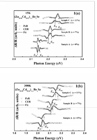
Figure 1. CER and PzR spectra for three different compositions of ZnCdBeSe samples in spectral range between 1.9 and 2.4 eV at (a) 15 K and (b) 300 K.
Figure 2. PzR spectra for E || [110] of Ga0.46In0.54N0.01P0.99
(Sample C) at several temperatures between 15 and 300 K.
The dashed lines are the experimental curves and the solid lines are least-squares fits to Lorentzian line shape.
IV
Figure 3. PzR spectra for E ||[110] of Ga0.46In0.54N0.01P0.99
(Sample C) at several temperatures between 15 and 300 K.
The dashed lines are the experimental curves and the solid lines are least-squares fits to Lorentzian line shape.
Fig 4. The temperature variations of Eg, Eg+∆12 and Eg+∆13 for(a) Ga0.46In0.54P (Sample A), (b) Ga0.46In0.54N0.005P0.995
(Sample B), and (c) Ga0.46In0.54N0.01P0.99 (Sample C) with representative error bars. The solid curves are least- squares fits to the Varshni-type semiempirical relationship and the dotted lines are fitted to the Bose-Einstein-type expression.
FIG. 5. Experimental PL spectra (close circles) and PR (open squares) at 300 K for the three
Ga0.69In0.31NxAs1−x /GaAs SQWs in the energy range 0.85–1.75 eV. Clear Franz-Keldysh oscillations above 1.4 eV are displayed in the PR spectra. The least-squares fits to the first-derivative line shape functions are shown as solid curves. The obtained intersubband energies denoted as A–I, respectively, for 11H, 12 H, 11 L, 21 H, 22 H, 21 L, 31 H, 32 H, and 34 H transitions are marked by arrows below the features.
FIG. 6. The PR spectra in the spectral range of excitonic transitions for (a) sample A and (b) sample B at 10, 30, 77, 100, 150, 200, 250, and 300 K. To facilitate comparison of spectra at different temperatures, a lateral shift of the spectra with respect to the 11H transition is performed.
The zero energy scale on the abscissa corresponds to the location of the 11H transition. The obtained intersubband energies are denoted by letters A–H and marked by arrows below the features.
V
FIG. 7. Temperature dependence of the various excitonic transition energies for sample B. The solid and dotted lines are least squares fits to Varshni and Bose-Einstein
equation, respectively. Representative error bars are shown for the experimental data.
FIG. 8. The 11H excitonic transition obtained from PR spectra and PL peak position of the three
Ga0.69In0.31NxAs1−x /GaAs SQW samples in
temperature range of 10–300 K. Representative error bars for the experimental data are indicated. The solid lines are least-squares fits.
Fig. 9. Presents room temperature angle-dependent R spectra..
Fig. 10. Presents room temperature angle-dependent SPV spectra.
VI
Fig. 11. Presents room temperature angle-dependent DSPV spectra.
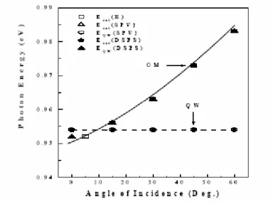
Fig. 12. Shows the results of room temperature angle- dependent DSPS, SPS and R measurements
Fig. 13. Shows the results of the temperature-dependent DSPS, SPS and R measurements
VII
![Figure 3. PzR spectra for E || [ 1 1 0 ] of Ga 0.46 In 0.54 N 0.01 P 0.99](https://thumb-ap.123doks.com/thumbv2/9libinfo/9126125.410462/7.892.474.787.95.470/figure-pzr-spectra-e-ga-n-p.webp)