Digital-Controlled Power Factor Corrector with Transition Current Mode Control without Zero
Current Detection
Chia-An Yeh, Kung-Min Ho, Yen-Shin Lai Center for Power Electronics Technology, National Taipei University of Technology
Taipei, Taiwan, R.O.C.
Fumikazu Takahashi, Masahiro Hamaogi Hitachi Computer Peripheral Co. Ltd., Japan
Japan
Abstract -It is well known that transition current mode
control for power factor corrector can reduce the reversal recovery loss for the diode. This method can be realized using discrete control integrated circuit which requires zero-crossing detection circuit. In this paper, a novel control technique for digital-controlled power factor corrector to achieve transition current mode control is proposed. The switching period to retain zero current switching is predicted and the turn-on period is determined by the voltage controller.
Experimental results derived from a DSP-based controller are presented for confirmation. The power factor corrector is with 100 V/AC input and 400 V/DC output. Its power rating is 250 W. Experimental results show that the power factor is higher than 0.98, efficiency is greater than 94% and current total harmonics distortion (THDi) is smaller than 4% under full load condition and confirms the above-mentioned claims very well.
Keywords-
power factor corrector; transition current mode
;digital control
I. I
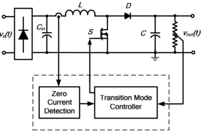
NTRODUCTIONPower factor correction technique has been widely used in AC to DC switching mode power system to meet the requirement of international standards. The PFC can reduce the harmonics of line current and improve power factor by unity power factor control. In order to achieve unity power factor and high efficiency, several topologies and control methods are analyzed [1-9]. The reduction of reversal recovery loss of diode is one of the most intensive research topics. One way is to use silicon carbide diode at the expense of more cost [3-4]. An alternative approach is to turn-on the power device with zero current switching by transition current mode control [5-8]. For conventional transition current mode control as shown in Fig. 1, zero-current detection is required in conventional analog implementation. Zero-crossing detection can be achieved using in-series resistor, Hall sensor, or coupled inductor. For transition current mode control method, the inductor current and duty are shown in Fig 2. As shown in Fig.2, the power device is turned on as inductor
current equal to zero and thereby reducing the reversal recovery loss of diode. The power device is turned at the beginning of every switching period, retained during the on-time period which is controlled by voltage loop controller, and turned off when the inductor current becomes zero.
Fig.1Conventional transition current mode controlled PFC converter
Fig. 2 Typical inductor current and duty waveforms
Digital control is with some advantages, including less discrete-component count, no aging issue for the compensator components, higher flexibility and fast time-to-market.
Therefore, digital power has received more and more attention for research and industrial applications [9]. In this paper, a novel control technique for digital-controlled power factor corrector to achieve transition current mode control without zero-current detection is proposed. The switching period to achieve zero current switching is predicted and the turn-on period is determined by the voltage controller. Experimental results derived from a DSP-based controller are presented for confirmation.
II. P
ROPOSEDD
IGITAL-C
ONTROLLEDT
RANSITIONC
URRENTM
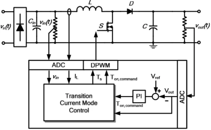
ODEFigure 3 shows the proposed digital-controlled transition current mode PFC boost converter system. As shown in Fig.3, the voltage error between the reference and its feedback value gives the on-time command via PI controller. The switching period will be predicted by proposed control method and the duty cycle can be determined according to predicted switching period and on-time command.
Fig. 3 Digital controlled PFC converter
Fig.4 shows the relationship among sampled current ( I
L[n] ),sampling instant and duty. As shown in Fig. 4, an error between the reference and inductor current (solid line) under transient condition can be removed by controlling the switching period properly. More details of the deduction of the predictive duty are as follows. Under steady state, the (n+1)
thon-time command is the same as that of its previous one as shown by:
[ 1] [ ]
on on
T n + = T n (1)
Since the switching frequency for PFC control is greater than the line frequency, the following condition can be assumed as:
[ 1] [ ]
s s
T n + ≅ T n (2)
By (1) and (2), the (n+1)
thoff-time is the same as that of the
(n)
thoff-time shown in (3).
[ 1] [ ]
off off
T n + ≅ T n (3)
In order to achieve zero current switching, the control function can be derived from Fig.4:
1 2
[ ] [ ] [ ] 0
2
on
L off
I n + m T n − m T n = (4)
where
th th
th
1 2
[ ] the n sampled average inductor current [ ] the n on time
[ ] the n off time on-time current slope
off-time current slope
L on off
I n T n T n m m
=
=
=
=
=
The (n)
thoff-time can be obtained by (4) as:
1
2 2
[ ] 1 [ ] [ ]
off L
2
onT n I n m T n
m m
= + (5)
According to (3) the (n+1)
thoff-time can be derived as:
1
2 2
[ 1] 1 [ ] [ ]
off L
2
onT n I n m T n
m m
+ = + (6)
The (n+1)
thswitching period can be determined by:
1
2 2
[ 1] 1 [ ] (1 ) [ ]
s L
2
onT n I n m T n
m m
+ ≅ + + (7)
In PFC boost converter, the current slopes are:
1
ˆ sin
in in[ ] V t V n
m L L
= ω = (8)
2
ˆ sin [ ] [ ]
out in out in
V V t V n V n
m L L
ω
− −
= = (9)
Where
ˆ
inpeak value of input voltage V =
[ ] n sampled input voltage
thV n
in=
[ ] n sampled output voltage
thV
outn =
input inductor L =
By (7)-(9), the switching period for transition current mode
control is given by:
[ 1] [ ] [ ] [ ]
[1 [ ] ] [ ]
2( [ ] [ ])
s L
out in
in
on
out in
T n L I n
V n V n
V n T n
V n V n
+ = −
+ + ⋅
−
(10)
As shown in (10), the predictive switching period is determined by input voltage ( V
in), output voltage ( V
out), input inductor ( L ) and average inductor current ( I
L).
1 Vin
m=L m2 Vout Vin L
− = − −
Fig. 4 Relationship between sampled current ( IL[n] ) and sampling instant under transition current mode
IV. DSP-
BASEDI
MPLEMENTATION OFP
ROPOSEDC
ONTROLT
ECHNIQUEIn this section, the maximum value of carrier will be defined. Fig.5 shows the relationship among carrier, duty, inductor current and sampling instant under transition current mode. As shown is Fig.5, triangular modulation is used to produce the duty cycle and the peak value of carrier for triangular modulation is:
[ ] [ ]
2
s m
CLK T n
V n = ⋅ (11)
The on-time command derived from the voltage loop control is:
_
[ ] [ ]
2
on on com
CLK T n
T n = ⋅ (12)
Where
_
[ ] on-time value, the sample [ ] on-time command, the sample [ ] DPWM counter peak value, the sample
DSP clock frequency = 150MHz
th on
th on com
th m
T n n
T n n
V n n
CLK
=
=
=
=
For DSP-based implementation, the carrier command, V
m, and on-time command, T
on_com, should be calculated by the restart
instant of carrier counter, t
n+1, as shown in Fig.5. Therefore, the carrier command, V
m[n+1], derived by (10)-(12) can berewritten as:
_
[ 1]
[ 1]
2
2( [ ] [ ]) [ ]
(1 [ ] ) [ ]
2( [ ] [ ])
s m
L
out in
in
on com
out in
CLK T n V n
CLK L V n V n I n
V n T n
V n V n
⋅ +
+ =
= ⋅
−
+ + ⋅
−
(13)
L( ) i t
Fig.5 Relationship between carrier, duty, inductor current and sampling instant under transition current mode
V. E
XPERIMENTALS
YSTEM ANDR
ESULTSThe specifications of the digital-controlled AC/DC converter are shown in Table I. The input voltage is 100 V AC and the output voltage is 400 V DC. The switching frequency varies from 30 kHz to 100 kHz. Fig. 6 shows the block diagram of the experimental system and the photo of the experimental system. A digital signal processor is used as the digital controller to realize the transition current mode PFC control in software.
Table I Specifications of PFC converter Specification
Input Voltage 100Vac/50Hz
Output Voltage 400Vdc
Output Power 250W
Switching Frequency 30kHz ~ 100kHz
Inductor value 410μH
Capacitor value 330μF
Control device TMS320F2812
(A) Block diagram
(B) Photo of experimental system
Fig. 6 Experimental system
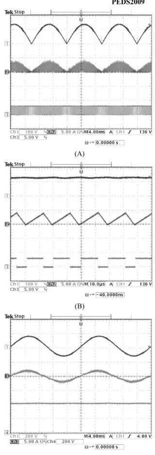
Fig. 7(A) shows the experimental results, including input voltage, inductor current and PWM signal waveforms under half load condition. As shown in Fig. 7 (B), the main switch is turned on as inductor current is zero. As shown in Fig. 7 (C), the input current and voltage are in phase confirming good power factor. Similarly, Fig. 8 shows the experimental results under full load condition confirming the effectiveness of the proposed digital-controlled TCM PFC. The measured power factor is shown in Fig. 9 (A). As shown in Fig. 9 (A), the power factor is greater than 0.99 under full load condition. Fig.
9 (B) shows the measured results of efficiency. The efficiency is greater than 93% under various kinds of load conditions.
Fig. 9(C) shows the measured results of current THD. The current THD is smaller than 4% under full load condition.
These experimental results demonstrate the effectiveness of the proposed digital-controlled TCM PFC converter.
(A)
(B)
(C)
Fig.7 Experimental results, Ch1: Input voltage, Ch2: Inductor current, Ch3:
Switching signal for (A) and (B); Ch1: Input voltage, Ch3: Input current, Ch4:
Output voltage for (C) (Vin=100V, Vout=400V, Pout=125W)
(A)
(B)
(C)
Fig.8 Experimental results, Ch1: Input voltage, Ch2: Inductor current, Ch3:
Switching signal for (A) and (B); Ch1: Input voltage, Ch3: Input current, Ch4:
Output voltage for (C) (Vin=100V, Vout=400V, Pout=250W)
0.9 0.92 0.94 0.96 0.98 1 1.02
50 100 150 200 250
Output power (W)
Power factor
(A) Power factor
90 91 92 93 94 95 96 97 98
50 100 150 200 250
Output power (W)
Efficiency (%)
(B) Efficiency
0 2 4 6 8 10 12 14 16
50 100 150 200 250
Output power (W)
THDi(%)
(C) THDi
Fig.9 Experimental results
VI. CONCLUSION
This paper proposes a predictive control technique for
digital-controlled power factor corrector to achieve transition
current mode control. The special features of the proposed
predictive control technique includes not requiring
zero-crossing detection of current and no need of fast A/D converter and sampling of current for current sensing.
Moreover, an on-time compensation technique is also proposed in this paper to cope with the current sharing issue caused by the parameter variation between interleaved TMCPFC.
Experimental results derived from a DSP-based controller are presented for confirmation. The power factor corrector is with 100 V/AC input and 400 V/DC output. Experimental results show that for single phase, the power factor is higher than 0.98, efficiency is greater than 94% and current total harmonics distortion (THDi) is less than 4% under full load condition.
A
CKNOWLEDGEMENTThis work is sponsored by Hitachi Computer Peripheral Co.
Ltd. and Hitachi Research Lab., Japan.
R
EFERENCE[1] B. Singh, B.N. Singh, A. Chandra, K. Al-Haddad, A. Pandey and D.P.
Kothari, “A review of single-phase improved power quality AC-DC converters,” IEEE Trans. on Industrial Electronics, Vol. 50, No.5, pp.962 – 981, OCT., 2003
[2] M. M. Jovanovic´, and Y. Jang, “State-of-the-Art, Single-Phase, Active Power-Factor-Correction Techniques for High-Power Applications—An Overview.” IEEE Trans. on Industrial Electronics, Vol. 52, No.3, pp.701 – 708, June, 2005
[3] P. Das, A. Mousavi, G. Moschopoulos and P. Jain, “A study of ac-dc ZVS-PWM boost converters with silicon carbide diodes,” IEEE APEC, pp.1158 – 1164, Feb., 2009.
[4] M. Janicki, D. Makowski, P. Kedziora, L. Starzak, G. Jablonski and S. Bek,
“Improvement Of PFC Boost Converter Energy Performance Using Silicon Carbide Diode,” IEEE MIXDES, pp.615 – 618, June, 2006.
[5] T.F. Wu, J.R. Tsai, Y.M. Chen and Z.-H. Tsai, “Integrated Circuits of a PFC Controller for interleaved critical mode boost converters,” IEEE APEC, pp.1347-1350, Mar., 2007.
[6] L. Huber, B. T. Irving and M. M. Jovanovic, “Open-loop control methods for interleaved DCM/CCM boundary boost PFC converters,” IEEE Trans.
on Power Electronics, Vol. 23, No. 4, pp. 1649 – 1657, July, 2008.
[7] J. W. Kim, S. M. Choi and K. T. Kim, ”Variable on-time control of the critical conduction mode boost power factor correction converter to improve zero-crossing distortion, ” IEEE PEDS, pp.1542-1546, Nov., 2005.
[8] J. Zhihong and L. Hui, “DSP Control of interleaving critical PFC module for high power application,” IEEE IECON, pp. 712-716, Nov., 2008.
[9] Z. Z. Ye and M. M. Jovanovic, ”Implementation and performance evaluation of DSP-based control for constant-frequency discontinuous-conduction-mode boost PFC front end,” IEEE Trans. on Industrial Electronics, Vol. 52, pp.98 – 107, Feb., 2005.
![Fig. 4 Relationship between sampled current ( I L [n] ) and sampling instant under transition current mode](https://thumb-ap.123doks.com/thumbv2/9libinfo/9124242.408736/3.892.469.827.142.615/fig-relationship-sampled-current-sampling-instant-transition-current.webp)