國
立
交
通
大
學
電子工程學系 電子研究所
博 士 論 文
電感耦合電漿氮化製程與氟化製程對鉿系高介電常數材料薄
膜之效果
The Effect of Inductively-Coupled Plasma Nitridation and Fluorination Process to
Hf-based Dielectric Thin Films
研 究 生:陳柏寧
指導教授:張國明 教授
電感耦合電漿氮化製程與氟化製程對鉿系高介電常數材料薄
膜之效果
The Effect of Inductively-Coupled Plasma Nitridation and Fluorination Process to
Hf-based Dielectric Thin Films
研 究 生:陳柏寧 Student:Bwo-Ning Chen
指導教授:張國明 Advisor:Kow-Ming Chang
國 立 交 通 大 學
電子工程學系 電子研究所
博 士 論 文
A DissertationSubmitted to Department of Electronics Engineering and Institute of Electronics
College of Electrical and Computer Engineering National Chiao Tung University
in partial Fulfillment of the Requirements for the Degree of
Doctor of Philosophy in
Electronics Engineering
July 2010
Hsinchu, Taiwan, Republic of China
中華民國九十九年七月
電感耦合電漿氮化製程與氟化製程對鉿系高介電常數材料
薄膜之效果
學生: 陳柏寧 指導教授: 張國明 博士 國立交通大學 電子工程學系電子研究所中文摘要
在這篇論文中,我們致力於討論應用電感耦合電漿源對鉿系高介電常數材料作電漿 氮化處理的應用,以期達到改善鉿系高介電常數材料之電特性,可靠度與熱穩定性之目 的,然後再我們嘗試加入電感耦合電漿氟化處理的製程,以期進一步改善之前電漿氮化 處理的效果,在我們的研究中,在調整到適合的實驗條件之下,電漿氮化與氟化製程的 結合可以改善二氧化鉿(HfO2)與及氧化鉿鋁(HfAlOx)的電特性與可靠度。 首先,我們先專注於討論電感耦合電漿氮化製程對二氧化鉿高介電常數材料薄膜的 效果,為了阻止雜質擴散,改善熱穩定度和增加鉿系閘極介電層介電常數之目的,利用 氮化製程將氮摻雜入閘極介電質材料,這類的技術已被廣泛的研究,我們利用電感耦合 電漿氮化製程以完成將氮摻雜進入二氧化鉿薄膜,實驗結果顯示二氧化鉿薄膜的電特 性,可靠度與熱穩定度可以藉由電漿氮化製程而得到改善,在我們實驗步驟中,電漿製 程之後整合了一個熱退火製程以減少由於電漿製程所帶給閘極介電層薄膜的傷害。 其次,因為二氧化鉿的熱穩定性不足以適應一般互補式金氧半導體元件製程,所以 半導體元件製程中的熱製程,如源極/汲極的活化,將會使二氧化鉿作為閘極介電層材料時發生漏電流增加以及橫向不均勻等問題,為了增加二氧化鉿材料的熱穩定性,將鋁 摻雜進入二氧化鉿形成氧化鉿鋁是一個有效的方法,因此我們嘗試應用相似的電感耦合 電漿氮化技術於氧化鉿鋁薄膜上,實驗結果,氧化鉿鋁的薄膜可以因為氮化而進一步改 善其電特性,可靠度與熱穩定度。 最後,摻雜氟進入二氧化鉿閘極介電層可以改善金屬氧化物半導體元件結構的種種 特性,如臨界電壓不穩,閘極漏電流,崩潰電壓和電容-電壓曲線的磁滯現象,沈積後 電漿處理技術已被研究用來摻雜氟進入二氧化鉿薄膜,在我們的研究中,我們結合了電 感耦合電漿氮化技術和電感耦合電漿氟化技術兩者,以氟化製程進一步改善氮化製程對 二氧化鉿和氧化鉿鋁的製程效果,增強其薄膜的電特性與可靠度。
The Effect of Inductively-Coupled Plasma Nitridation and
Fluorination Process to Hf-based Dielectric Thin Films
Student: Bwo-Ning Chen Advisor: Kow-Ming Chang Department of Electronics Engineering
& Institute of Electronics National Chiao-Tung University
Hsinchu, Taiwan R.O.C.
Abstract
In this dissertation, we concentrate our effect on applying plasma nitridation treatment in order to improve the electrical characteristics, the reliabilities and the thermal stability of Hf-based dielectric layers. Then we have tried to applied ICP fluorination process to enhance the improvement effect of the plasma treatment. The electrical characteristics and the reliabilities of HfO2 thin films and HfAlOx thin films could be modified in adequate process
conditions.
First, we are focus on the effect of ICP plasma nitridation process to the HfO2 thin films.
The incorporation of nitrogen into gate dielectrics by nitridation has been investigated with the aim of preventing dopant penetration, improving the thermal stability and enlarging the dielectric constant of Hf-based dielectrics. We use the plasma nitridation process to incorporate nitrogen into HfO2 thin films. The experimental result indicates that the electrical
characteristic, the reliability and the thermal stability of HfO2 thin films could be improved by
the plasma nitridation process. The post-nitridation annealing is integrated into the experimental steps for decreasing the plasma damage caused by the plasma treatment.
Secondly, since the thermal stability of the HfO2 dielectric layers is quite low, so the
thermal process, such as Source/Drain activation, would cause the high leakage current and lateral nonuniformity associated with grain boundaries after the deposition of HfO2 thin films.
In order to increase the crystallization temperature, Al could be added to HfO2 to form Hf
aluminates. We use similar plasma nitridation process to HfAlOx dielectric layers in order to
incorporate nitrogen. The electrical characteristic, the reliability and the thermal stability of HfAlOx thin films could be improved by the plasma nitridation process.
Finally, the incorporation of fluorine into the HfO2 gate dielectrics could improve the
MOS structure characteristics including threshold voltage instability, gate leakage current, breakdown voltage and C-V hysteresis. The post-deposition plasma fluorination has been used to incorporate fluorine into the HfO2 gate dielectrics. In our research, we combine the ICP
nitridation process and the ICP fluorination process to enhance the electrical characteristics and the reliability of HfO2 thin films and HfAlOx thin films.
致謝
首先在此感謝我的指導老師張國明教授,張國明老師在我這些年博士班以及碩士班 學習生涯中,在研究方面與待人處事方面上都給予許多的指導與幫助,本論文得以完成 首先要感謝老師不斷給我的支持。 在我這些日子的研究生活中,實驗室的學長同學與學弟們都給了我許多的幫助,特 別在此先感謝實驗室的楊文誌學長在這幾年的指導與關心,另外感謝陳巨峰學長,鄧一 中學長,曾明豪學長,游凱翔學長,王敬業學長,王漢邦學長,賴瓊惠學姐,林稔杰學 長,趙高毅學長,林俊銘學長,朱俊宜學長,林志祥學長,陳在泩學長,郭俊銘學長等 人在學術生活中前前後後的建議與關懷,感謝林建宏同學這些年大力地幫助與鼓勵,感 謝黃士軒學弟,張知天大哥,曾文賢學弟,黃菘宏學弟,張庭嘉學弟,何伯慶學弟的支 持,感謝葉星輝學弟,黃士銘學弟,湯鈞凱學弟,蘇明紳學弟,吳汶錦學弟,林協佑學 弟在實驗操作上的鼎力相助,還有許多實驗室學長同學與學弟在這本論文一點一滴的建 立中慷慨地給予了我很多的鼓勵,在此感謝。 另外感謝交通大學奈米中心以及國家奈米實驗室在實驗器材上的大力支持,感謝兩 個機構中許倬綸先生等許許多多的研究人員這些年提供的幫助。交通大學電子工程所的 各位教師與及林明霓小姐,李清音小姐等許多的行政人員,這些年來也不斷給予我許多 的指導,在這裡謹向各位致意。 感謝我的家人,我的母親,我的姊姊,我的妹妹,以及我的姊夫和外甥女,還有所 有不斷給予我幫助的各位家族成員與父執長輩,他們對我的耐心與支持是我能夠持續研 究以及完成博士論文的最重要動力,感謝他們一直以來無間斷地關懷與包容,最後,感 念我的父親,希望我所有的喜悅都與他共享。Contents
Chinese Abstract………...………...i English Abstract………..………...iii Acknowledgment………..………..v Contents………... vi Figure Captions……….………...ix Chapter 1 Introduction……….………...11.1 Background and Motivation………...1
1.1.1 The Application of High-k Dielectric in Modern IC Process……….………1
1.1.2 The Hf-based High-k Dielectric……….………...1
1.1.3 The Problems about Integration of High-k Dielectric………2
1.1.4 The Nitrogen Incorporation into Hf-based Thin Films……….………..2
1.1.5 The Different Ways of Incorporating Nitrogen into Hf-based Thin Films………….…3
1.1.6 The Fluorine Incorporation into Hf-based Thin Films……….………...3
1.1.7 Motivation……….………...4
1.2 Dissertation Organization………...4
Chapter 2 The Improvement Effect of the Plasma Nitridation Process to the Electrical Properties, the Reliability and the Thermal Stability of HfO2 thin films…………..…………12
2.1 Introduction……….………....12
2.2 Experimental……….………..13
2.3 Results and Discussion……….………...14
2.3.2 Reliability……….………....17
2.3.3 Thermal Stability……….……….…19
2.4 Summary……….………....20
Chapter 3 The Improvement Effect of the Plasma Nitridation Process to the Electrical Properties, the Reliability and the Thermal Stability of HfAlOx thin films……….36
3.1 Introduction……….………...36
3.2 Experimental……….………..37
3.3 Results and Discussion……….………...…38
3.3.1 The Most Suitable Process Time……….38
3.3.2 Reliability……….………40
3.3.3 Thermal Stability……….……….42
3.4 Summary……….………....43
Chapter 4 The Improvement Effect of the Plasma Nitridation Process and the Plasma fluorination Process to HfO2 thin films………57
4.1 Introduction………..……….………..57
4.2 Experimental……….………..58
4.3 Results and Discussion……….………...59
4.3.1 The Electrical Characteristics………..59
4.3.2 Reliability……….………61
4.3.3 Physical Analysis………62
4.4 Summary……….………....63
Chapter 5 The Improvement Effect of the Plasma Nitridation Process and the Plasma Fluorination to HfAlOx thin films………81
5.1 Introduction……….………....81
5.2 Experimental……….………..82
5.3 Results and Discussion……….………...…83
5.3.1 The Electrical Characteristics………..83
5.3.2 Reliability……….………85
5.3.3 Physical Analysis………87
5.4 Summary……….………87
Chapter 6 Conclusion and Future Work………104
6.1 Conclusion………104
6.2 Future Work……….……….105
References………107
Figure Captions
Chapter 1
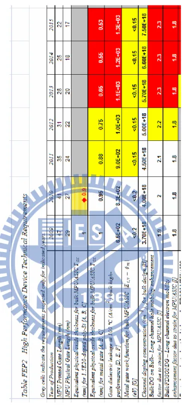
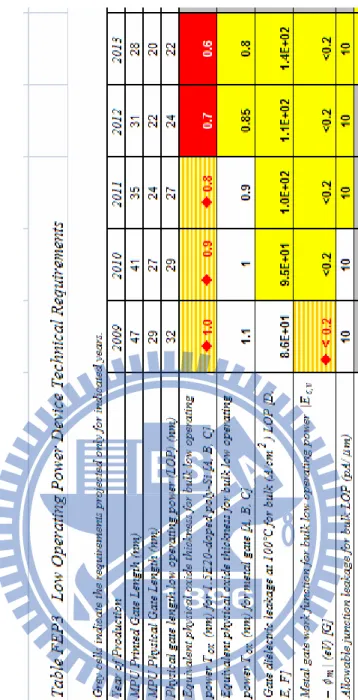
Fig. 1.1 The partial table from ITRS 2009, which indicates the predicted standard for high performance (HP) device technical requirements. ……….6 Fig. 1.2 The partial table from ITRS 2009, which indicates the predicted standard for low
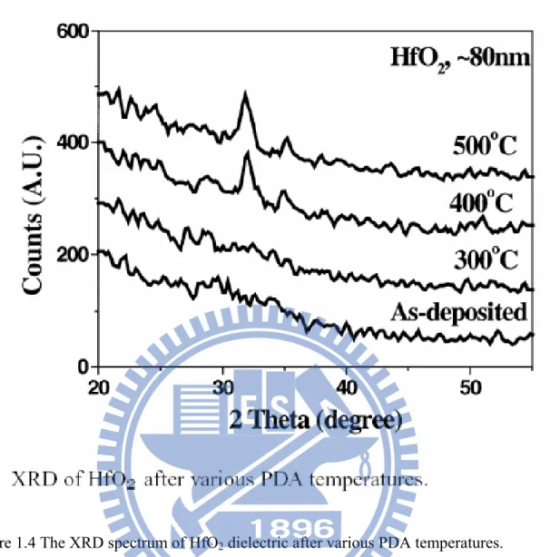
operating power (LOP) device technical requirements. . ………...7 Fig. 1.3 The partial table from ITRS 2009, which indicates the predicted standard for low standby power (LSTP) device technical requirements…...………..8 Fig. 1.4 The XRD spectrum of HfO2 dielectric after various PDA temperatures………9
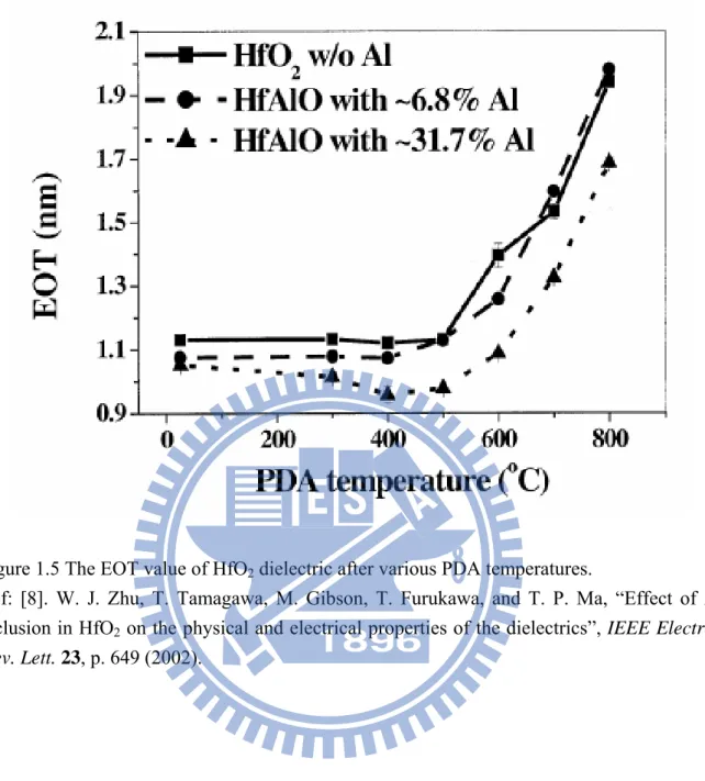
Fig. 1.5 The EOT value of HfO2 dielectric after various PDA temperatures..………...……10
Fig. 1.6 The plasma source of the plasma enhanced chemical vapor deposition (PECVD) system and inductively-coupled plasma (ICP) system…...………...………11
Chapter 2
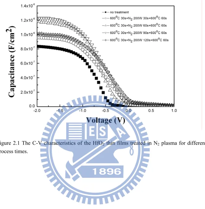
Fig. 2.1 The C-V characteristics of the HfO2 thin films treated in N2 plasma for different process
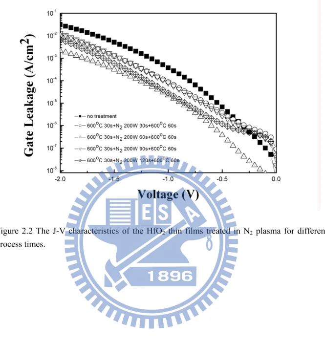
times..………....21 Fig. 2.2 The J-V characteristics of the HfO2 thin films treated in N2 plasma for different process
times..………....22 Fig. 2.3 The C-V characteristics of the HfO2 thin films treated in NH3 plasma for different
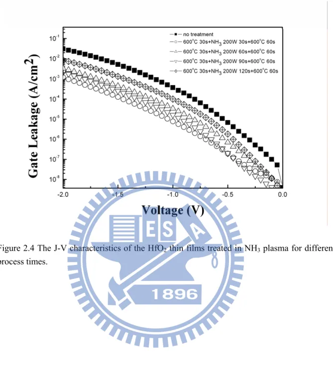
process times.………....23 Fig. 2.4 The J-V characteristics of the HfO2 thin films treated in NH3 plasma for different process
times..………....24 Fig. 2.5 The C-V characteristics of the HfO2 thin films treated in N2O plasma for different
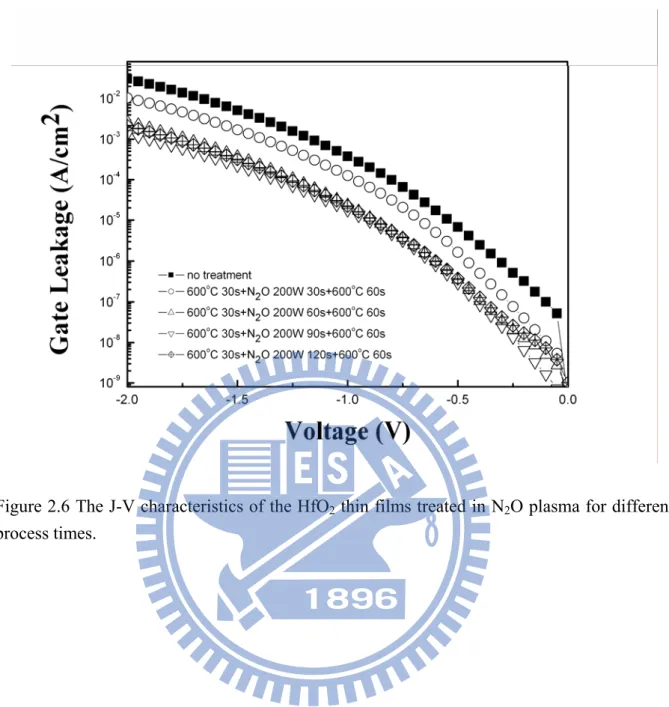
Fig. 2.6 The J-V characteristics of the HfO2 thin films treated in N2O plasma for different process
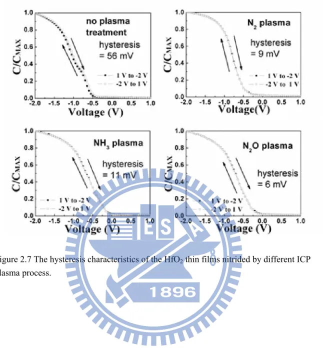
times..………....26 Fig. 2.7 The hysteresis characteristics of the HfO2 thin films nitrided by different ICP plasma
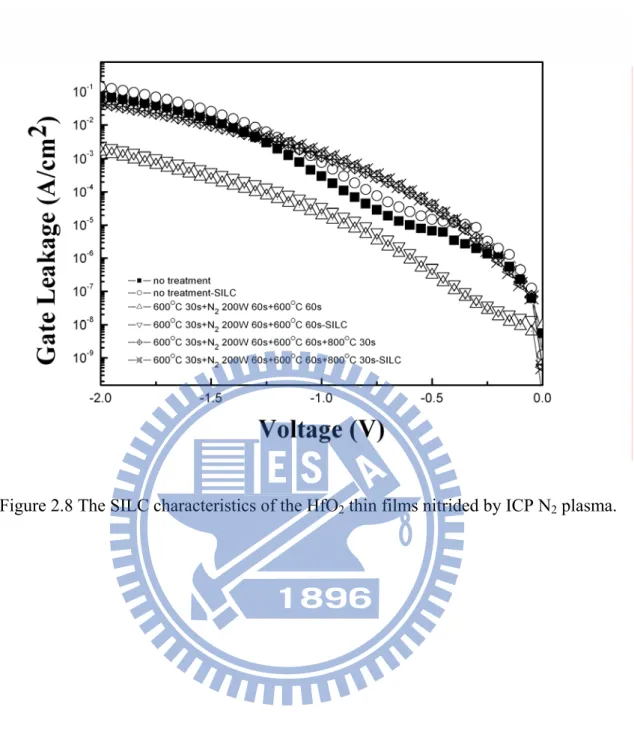
process..………....27 Fig. 2.8 The SILC characteristics of the HfO2 thin films nitrided by ICP N2 plasma...28
Fig. 2.9 The SILC characteristics of the HfO2 thin films nitrided by ICP NH3 plasma………….29
Fig. 2.10 The SILC characteristics of the HfO2 thin films nitrided by ICP N2O plasma………….30
Fig. 2.11 The leakage current shift curves of the HfO2 thin films nitrided by ICP N2 plasma……31
Fig. 2.12 The leakage current shift curves of the HfO2 thin films nitrided by different plasma…..32
Fig. 2.13 The C-V characteristics of the HfO2 gate dielectrics treated by different plasma
nitridation process and PDA……….33 Fig. 2.14 The J-V characteristics of the HfO2 gate dielectrics treated by different plasma
nitridation process and PDA……….34 Fig. 2.15 The XPS analysis of the Hf 4f electronic spectra of the samples treated in ICP N2 plasma
for 60 sec. ..………...35
Chapter 3
Fig. 3.1 The C-V characteristics of the HfAlOx thin films treated in N2 plasma for different
process times………...44 Fig. 3.2 The J-V characteristics of the HfAlOx thin films treated in N2 plasma for different
process times. ..………..………...45 Fig. 3.3 The C-V characteristics of the HfAlOx thin films treated by different kinds of plasma...46
Fig. 3.4 The J-V characteristics of the HfAlOx thin films treated by different kinds of plasma…47
Fig. 3.5 The hysteresis characteristics of the samples nitrided by different kinds of plasma containing nitrogen….………...48 Fig. 3.6 The SILC characteristics of the HfAlOx thin films nitrided by N2 plasma………...49
Fig. 3.7 The SILC characteristics of the HfAlOx thin films nitrided by NH3 plasma………50
Fig. 3.8 The SILC characteristics of the HfAlOx thin films nitrided by N2O plasma………51
Fig. 3.9 The leakage current shift curves of the HfAlOx thin films nitride by N2 plasma……….52
Fig. 3.10 The leakage current shift curves of the HfAlOx thin films nitride by NH3 plasma……..53
Fig. 3.11 The leakage current shift curves of the HfAlOx thin films nitride by N2O plasma……..54
Fig. 3.12 The C-V characteristics of the HfAlOx gate dielectrics treated by different plasma
nitridation process, PDA and high temperature process…...………55 Fig. 3.13 The J-V characteristics of the HfAlOx gate dielectrics treated by different plasma
nitridation process, PDA and high temperature process………...56
Chapter 4
Fig. 4.1 The C-V characteristics of the HfO2 thin films treated in N2 plasma for 60 sec and then in
CF4 plasma for different process times. ..……….…65
Fig. 4.2 The J-V characteristics of the HfO2 thin films treated in N2 plasma for 60 sec and then in
CF4 plasma for different process times...………..66
Fig. 4.3 The C-V characteristics of the HfO2 thin films treated in NH3 plasma for 90 sec and then
in CF4 plasma for different process times...………67
Fig. 4.4 The J-V characteristics of the HfO2 thin films treated in NH3 plasma for 90 sec and then
in CF4 plasma for different process times....……….68
Fig. 4.5 The C-V characteristics of the HfO2 thin films treated in N2O plasma for 90 sec and then
in CF4 plasma for different process times...………..69
Fig. 4.6 The J-V characteristics of the HfO2 thin films treated in N2O plasma for 90 sec and then
in CF4 plasma for different process times. ...………70
Fig. 4.7 The hysteresis characteristics of the HfO2 thin films without plasma treatment………..71
Fig. 4.8 The hysteresis characteristics of the HfO2 thin films treated in N2 plasma for 60 sec and
Fig. 4.9 The hysteresis characteristics of the HfO2 thin films treated in NH3 plasma for 90 sec and
then in CF4 plasma for 60 sec...………...73.
Fig. 4.10 The hysteresis characteristics of the HfO2 thin films treated in N2O plasma for 90 sec and
then in CF4 plasma for 60 sec. ...………..74
Fig. 4.11 The leakage current shift curves of the HfO2 thin films that were nitrided by ICP N2
plasma for 60 sec then fluorinated by ICP CF4 plasma for different time………75
Fig. 4.12 The leakage current shift curves of the HfO2 thin films that were nitrided by ICP NH3
plasma for 90 sec then fluorinated by ICP CF4 plasma for different time………76
Fig. 4.13 The leakage current shift curves of the HfO2 thin films that were nitrided by ICP N2O
plasma for 90 sec then fluorinated by ICP CF4 plasma for different time………77
Fig. 4.14 The SIMS profile of the HfO2 thin films treated in ICP N2 plasma for 60 sec and treated
in ICP CF4 plasma for 60 sec. ...………...78
Fig. 4.15 The XPS F 1s electronic spectra of the HfO2 thin films treated in ICP N2 plasma for 60
sec and treated in ICP CF4 plasma for 60 sec...………79
Fig. 4.16 The XPS analysis of the Hf 4f electronic spectra of the samples treated in ICP CF4
plasma for 60 sec………...80
Chapter 5
Fig. 5.1 The C-V characteristics of the HfAlOx thin films treated in N2 plasma for 30 sec and then
in CF4 plasma for different process times. ...………89
Fig. 5.2 The J-V characteristics of the HfAlOx thin films treated in N2 plasma for 30 sec and then
in CF4 plasma for different process times. ...………90
Fig. 5.3 The C-V characteristics of the HfAlOx thin films treated in NH3 plasma for 30 sec and
then in CF4 plasma for different process times...………..91
Fig. 5.4 The J-V characteristics of the HfAlOx thin films treated in NH3 plasma for 30 sec and
Fig. 5.5 The C-V characteristics of the HfAlOx thin films treated in N2O plasma for 30 sec and
then in CF4 plasma for different process times. ...………93
Fig. 5.6 The J-V characteristics of the HfAlOx thin films treated in N2O plasma for 30 sec and
then in CF4 plasma for different process times. ...………94
Fig. 5.7 The hysteresis characteristics of the HfAlOx thin films without plasma treatment……..95
Fig. 5.8 The hysteresis characteristics of the HfAlOx thin films treated in N2 plasma for 30 sec
and then in CF4 plasma for 60 sec. ...………96
Fig. 5.9 The hysteresis characteristics of the HfAlOx thin films treated in NH3 plasma for 30 sec
and then in CF4 plasma for 60 sec...………..97
Fig. 5.10 The hysteresis characteristics of the HfO2 thin films treated in N2O plasma for 30 sec and
then in CF4 plasma for 60 sec. ...………..98
Fig. 5.11 The leakage current shift curves of the HfAlOx thin films that were nitrided by ICP N2
plasma for 30 sec then fluorinated by ICP CF4 plasma for different time………99
Fig. 5.12 The leakage current shift curves of the HfAlOx thin films that were nitrided by ICP NH3
plasma for 30 sec then fluorinated by ICP CF4 plasma for different time………..100
Fig. 5.13 The leakage current shift curves of the HfAlOx thin films that were nitrided by ICP N2O
plasma for 30 sec then fluorinated by ICP CF4 plasma for different time………..101
Fig. 5.14 The SIMS profile of the HfAlOx thin films treated in ICP N2O plasma for 30 sec and
treated in ICP CF4 plasma for 30 sec………..102
Fig. 5.15 The XPS F 1s electronic spectra of the HfAlOx thin films treated in ICP N2O plasma for
Chapter 1
Introduction
1.1 Background and Motivation
1.1.1 The Application of High-k Dielectric in Modern IC Process
The continuing downsizing of silicon device has significantly reduced the thickness of the gate dielectric film. However, dielectric layer scaling companies the excessive off-state leakage current that would cause intolerable power consumption and overheat of the devices. To solve the issue about leakage current, a major resolution is to replace the silicon dioxide with a thicker dielectric layer that has a higher dielectric constant and maintains relatively low equivalent oxide thickness (EOT) [1.1]. Fig. 1.1 is the partial table from ITRS 2009, which indicates the predicted standard for high performance (HP) device technical requirements. According to this table, EOT of 0.75 nm is essential for 22 nm HP device technical CMOS technology. Fig. 1.2 and Fig 1.3 are also partial tables from ITRS 2009, which indicate the predicted standard for low operating power (LOP) device technical requirements and low standby power (LSTP) device technical requirements, respectively. In the LOP and LSTP device standard of 2012, even with integration of metal gate process, the EOT of dielectric layers would at least shrink to 1.0 nm. The above fact indicates the necessary to apply high-k dielectrics in CMOS process flow.
1.1.2 The Hf-based High-k Dielectric
dielectrics have emerged as the promising candidates to replace the ultrathin silicon dioxide dielectrics for the advanced CMOS technologies [1.2-1.5]. Among these dielectrics, HfO2 is
considered as a suitable gate dielectric material because of the acceptable band gap (~ 5.7 eV), the large dielectric constant (~ 25) and relatively high free energy of reaction with Si (47.6 kcal/mole at 727 oC) [1.6].
1.1.3 The Problems about Integration of High-k Dielectric
However, there are still several challenges which have to be considered in order to integrate these high-k dielectrics into a conventional CMOS process flow such as the interface SiO2 regrowth and the thermal stability of these dielectrics [1.7]. The crystallization
temperature of HfO2 is quite low, so the thermal process, such as Source/Drain activation,
would cause the high leakage current and lateral nonuniformity associated with grain boundaries after the deposition of HfO2 thin films. The incorporation of Al in Hf-based
dielectrics has been proven as an effective solution to the issue of thermal stability [1.8]. Fig. 1-4 shows that crystallization of pure HfO2 dielectric would happen between 300 oC to 400 oC.
Fig. 1-5 presents that with incorporation of Al in HfO2 thin films, the EOT change of
Hf-based dielectrics through thermal processes could be suppressed. The above experimental results prove the thermal stability of HfO2 thin films could be improved by inducing Al in to
thin films.
1.1.4 The Nitrogen Incorporation into Hf-based Thin Films
In high-k dielectrics, there is a high density of charge traps that could cause instability of the threshold voltage, Coulomb scattering of carriers in the channel and reliability problems. The main part of the charge traps is thought to be from oxygen vacancy in the hafnium-based
dielectric [1.9]. Nitrogen incorporation is the widely accepted technique to passivate those defects [1.10-1.11]. In the meantime, nitridation was also beneficial because nitridation decreased hot electron degradation, perhaps because nitrogen lessens the diffusion of hydrogen in the oxide [1.12]. The incorporation of nitrogen into gate dielectrics by nitridation also has been investigated with the aim of preventing dopant penetration [1.13-1.14]. Recently, the various nitridation processes have been shown to improve the thermal stability and the dielectric constant of Hf-based dielectrics [1.15-1.20]. Besides, the nitridation process also has been shown to improve the thermal stability of Hafnium-silicate thin films [1.21].
1.1.5 The Different Ways of Incorporating Nitrogen into Hf-based Thin Films
Thermal nitridation is usually performed at high temperature and hydrogen-containing species that act as electron traps could be added into the thin film. On the other hand, nitrogen could be incorporated into the dielectric layer by plasma nitridation process at lower temperature than by thermal nitridation process [1.22-1.23]. The source of plasma is various, in this dissertation, the inductively-coupled plasma (ICP) technology is used to incorporate nitrogen into Hf-based thin films. From Fig. 1-6, comparing to traditional plasma enhanced chemical vapor deposition (PECVD) system, the radical is firstly produced by ICP system then transport to surface of sample. So the radical density upon surface of sample in ICP system is higher than in traditional PECVD system. We could predict the effect of ICP plasma would be more apparent. The high density plasma effect is why we apply ICP technology in this dissertation.
1.1.6 The Fluorine Incorporation into Hf-based Thin Films
improve the MOS structure characteristics including threshold voltage instability, gate leakage current, breakdown voltage and C-V hysteresis [1.10]. After the incorporation of fluorine, fluorine could effectively passivate charge trapping sites at HfO2/SiO2 interface. Strong
hafnium-fluorine and silicon-fluorine bonds could be formed by fluorination [1.24-1.27]. Fluorine was found to substitute at the oxygen vacancy site and substitutional fluorine creates a shallow donor state [1.28-1.29]. As a result, the oxygen vacancy site could be passivated and the charged traps in high-k dielectric could be in stable state.
1.1.7 Motivation
In this research, firstly, we have tried to examine the plasma nitridation effect to the electrical properties, the reliabilities and the thermal stability of pure HfO2 thin films.
Secondly, we tried to apply the same plasma nitridation technology to HfAlOx thin films to
see if the electrical properties, the reliabilities and the thermal stabilities of HfAlOx thin films
could be modified by this plasma technology. Furthermore, we have tried to apply the plasma fluorination process to improve the characteristic of the nitrided HfO2 and HfAlOx thin films.
1.2 Dissertation Organization
In this dissertation, we concentrated our effort to examine the effect of the plasma nitridation process and the plasma fluorination process to the electrical characteristics, the reliability and the thermal stability of pure HfO2 and HfAlOx thin films.
In the chapter 1 of this dissertation, we describe the background and the motivation of our research. In the chapter 2, we apply the inductance-coupled plasma (ICP) nitridation technology to pure HfO2 thin films in order to improve the electrical characteristics, the
reliabilities and the thermal stability of pure HfO2 thin films. In the chapter 3, we examine the
similar ICP nitridation process to HfAlOx thin films to observe the process effect to the
electrical characteristics, the reliabilities and the thermal stability of HfAlOx thin films.
Furthermore, in the chapter 4, we use the ICP fluorination process to improve the electrical characteristic and the reliabilities of the plasma-nitrided HfO2 thin films. In the chapter 5, we
use the similar plasma fluorination process to improve the electrical characteristic and the reliabilities of the plasma-nitrided HfAlOx thin films.
Finally, in the chapter 6, a conclusion is given, and the future work about this dissertation is proposed.
Figure 1.1 The partial table from ITRS 2009, which indicates the predicted standard for high performance (HP) device technical requirements.
Ref: [1]. International Technology Roadmap for Semiconductors, presented at public.itrs.net (2009).
Figure 1.2 The partial table from ITRS 2009, which indicates the predicted standard for low operating power (LOP) device technical requirements.
Ref: [1]. International Technology Roadmap for Semiconductors, presented at public.itrs.net (2009).
Figure 1.3 The partial table from ITRS 2009, which indicates the predicted standard for low standby power (LSTP) device technical requirements.
Ref: [1]. International Technology Roadmap for Semiconductors, presented at public.itrs.net (2009).
Figure 1.4 The XRD spectrum of HfO2 dielectric after various PDA temperatures.
Ref: [8]. W. J. Zhu, T. Tamagawa, M. Gibson, T. Furukawa, and T. P. Ma, “Effect of Al inclusion in HfO2 on the physical and electrical properties of the dielectrics”, IEEE Electron
Figure 1.5 The EOT value of HfO2 dielectric after various PDA temperatures.
Ref: [8]. W. J. Zhu, T. Tamagawa, M. Gibson, T. Furukawa, and T. P. Ma, “Effect of Al inclusion in HfO2 on the physical and electrical properties of the dielectrics”, IEEE Electron
Figure 1.6 The plasma source of the plasma enhanced chemical vapor deposition (PECVD) system and inductively-coupled plasma (ICP) system.
Chapter 2
The Improvement Effect of the Plasma Nitridation Process
to the Electrical Properties, the Reliability and the
Thermal Stability of HfO
2thin films
2.1 Introduction
The rapid advancement of complementary metal oxide semiconductor (CMOS) field effect transistor process during the past few years has forced the microelectronics industry to face serious technological challenges. According to the predictions of the International Technology Roadmap for Semiconductor, the equivalent oxide thickness (EOT) and gate leakage currents of conventional gate dielectrics will reach their physical limits [1]. To solve the challenge about the excessive leakage current, many kinds of high-k dielectrics have emerged as the promising candidates to replace the ultrathin silicon oxynitride dielectrics for the advanced CMOS technologies [2-5]. The pure HfO2 is considered as a suitable gate
dielectric material because of the acceptable band gap, which is wide enough to avoid the gate leakage forming the unacceptable power consumption, and the large dielectric constant, which is big enough to increase the physical thickness of the gate dielectric and maintain the relatively low EOT. However, there are several issues which have to be considered in order to integrate these Hf-based dielectrics into a conventional CMOS process flow such as the reliability and the thermal instability of these dielectrics [7, 30-31]. The incorporation of nitrogen into gate dielectrics by nitridation has been investigated with the aim of preventing dopant penetration [13-14]. Recently, the various nitridation processes have been shown to improve the thermal stability and the dielectric constant of Hf-based dielectrics [15-18, 21].
However, thermal nitridation is usually performed at high temperature and hydrogen-containing species that act as electron traps could be introduced into the thin film by thermal nitridation process. On the other hand, nitrogen could be incorporated by plasma nitridation process into the dielectric layer at lower temperature than by thermal nitridation process [22, 32]. The objective of this report is to examine the effect of different ICP plasma nitridation process to the electrical characteristics, the reliability and the thermal stability of HfO2 thin films [33]. According to this study, the plasma nitridation process could be an
effective technology to improve the electrical characteristics, the reliability and the thermal stability of pure HfO2 thin films.
2.2 Experimental
In this research, Al/Ti/HfO2/Si structures were fabricated to investigate the effect of the
plasma nitridation to HfO2 dielectrics. A Si wafer with standard initial RCA cleaning was
placed into the chamber and a 6-nm HfO2 layer was deposited on the wafer by the MOCVD
system. Then the samples were annealed at 600 ℃ for 30 sec in pure N2 gas by rapid
temperature annealing (RTA) process and nitrided by an ICP plasma treatment at the substrate temperature of 300 ℃, the process pressure of the plasma nitridation process was set as 1.33 × 10⁻⁴ bar. Ar gas was added into the ICP chamber for activating the plasma while the nitridation process was performed. The flow rate of Ar was set as 10 sccm and the flow rate of the gas containing nitrogen, which is N2, NH3 or N2O, was set as 100 sccm. In an ICP system,
a rf current in the coils generates a changing magnetic field, then the magnetic field induces a changing electric field through inductive coupling. Therefore, the inductively coupled electric field accelerates electrons. The electronic mean free path might be shorter than the distance between the anode and the cathode, so there are enough ionizing collisions to produce high density plasma [34]. After the plasma nitridation, there was an annealing process whose
condition was at 600 ℃ for 30 sec in pure N2 to eliminate the plasma damage [35-36]. A Ti
film of 40 nm was deposited on the top side of the samples by sputtering. Then an Al film of 500 nm was thermally evaporated on the top side of the samples. The top electrodes were defined by a lithography process. Finally, the backside native oxide was stripped with diluted HF solution and the backside aluminum electrodes were evaporated by a thermal evaporation. The top area of the Al/Ti/HfO2/Si MOS capacitors is 5000 μm2. The capacitance-voltage
(C-V) and the current density-voltage (J-V) characteristics of the MOS structures were measured by semiconductor parameter analyzer (HP4156C) and C-V measurement (HP4284) in order to evaluate the improvement effect of the plasma nitridation process and the best process condition. The experimental condition of the stress induced leakage current (SILC) measurement that was carried out in this study was set as constant voltage of 3 V for 180 sec. The stress condition of constant voltage stress (CVS) measurement carried out in this study was set as constant voltage of 3 V to observe the change of the gate leakage current while the stress was applied.
2.3 Results and Discussion
In the beginning of this work, different process time was tested to decide the most suitable process condition for various plasma nitridation processes. After the process time had been determined, the improvement effect of the plasma nitridation process to the reliability of pure HfO2 thin films would be examined.
2.3.1 The Most Suitable Process Time
Figure 2.1 shows the C-V characteristics of the HfO2 gate dielectrics treated in ICP N2
measurement was set as 50 kHz. The capacitors treated for 90 sec perform the maximum capacitance density among these samples with different process times. The EOT of HfO2 thin
films decrease from 3.6 nm to 2.3 nm after N2 plasma nitridation. In addition, the capacitors
treated for 30 sec and 60sec also present the larger values than the capacitors without whole plasma nitridation process. The factor of improvement might be from that the PDA process [37-39] and the nitrogen incorporation in the HfO2 dielectrics, which could enhance the
electronic polarization as well as the ionic polarization, so the dielectric constant of the HfO2
thin films increases just as Hf-silicate thin films [20, 40] and SiO2 thin films [41]. Besides, the
capacitance density of the samples treated for 120 sec is degraded. The reason could be the damage caused by the N2 plasma.
The J-V characteristics of the HfO2 capacitors treated by ICP N2 plasma with different
process times from 0 V to -2 V are described in Fig. 2.2. The gate leakage current density is suppressed while the treatment condition was 60 sec. The reduction of the leakage current could be attributed to the post-deposition annealing process [37-38]. The gate leakage current density of the samples not treated in ICP N2 plasma at Vg of -1 V is about 3.74 × 10⁻⁴ A/cm2
and the gate leakage current density of the capacitors treated in ICP N2 plasma for 60 sec at
Vg of -1 V is about 2.22 × 10⁻⁵ A/cm2. Moreover, the leakage current densities of the samples
treated in N2 plasma for shorter or longer time are larger than the one treated for 60 sec. The
effect of the nitridation process with shorter process time might be not enough. On the other hand, while the nitridation process time is longer than 60 sec, the plasma damage from the plasma nitridation could cause the increase of the gate leakage density. In summary, the best process time of the plasma nitridation in N2 plasma is set as 60 sec. This appears that the
samples treated in N2 plasma for 60 sec display the most excellent value (the EOT of the
In Fig. 2.3 and Fig. 2.4, the C-V and the J-V characteristics of the HfO2 gate dielectrics
treated in ICP NH3 plasma for different process times are presented. As mentioned before, the
reason of the improvement effect in the NH3 plasma nitridation process could be the same as
the one in the N2 plasma nitridation process [20, 37]. From the similar analysis, the best
process time of the plasma nitridation in NH3 plasma is set as 90 sec. The EOT of HfO2 thin
films decrease from 3.6 nm to 2.3 nm after NH3 plasma nitridation. The gate leakage current
density of the capacitors treated in ICP NH3 plasma for 90 sec at Vg of -1 V is about 1.62 ×
10-5 A/cm2. This indicates that the samples treated in NH3 plasma for 90 sec displays the most
excellent value (the EOT of the samples is about 2.3 nm).
In Fig. 2.5 and Fig. 2.6, the C-V and the J-V characteristics of the HfO2 gate dielectrics
treated in ICP N2O plasma for different process times are demonstrated. There could be other
reasons for the improvement effect of the N2O plasma nitridation process. Since a high
concentration of oxygen vacancies causes electrons to be generated and a large leakage current to flow, treatment with plasma that contains oxygen could yield active oxygen atoms and reduce oxygen vacancies to improve the quality of dielectric films [34]. The EOT of HfO2
thin films decrease from 3.6 nm to 2.7 nm after N2O plasma nitridation. The gate leakage
current density of the samples treated in ICP N2O plasma for 60 sec at Vg of -1 V is about
2.37 × 10⁻⁵ A/cm2 and the gate leakage current density of the capacitors treated in ICP N2O
plasma for 90 sec at Vg of -1 V is about 2.22 × 10⁻⁵ A/cm2. So when the process time is set as
90 sec, the reduction of the gate leakage density of the nitrided sample would be more obvious. The decrease in the leakage current from nitridation process might be believed to be caused by electron trapping [42-43]. As mentioned above, the best process time of the plasma nitridation in N2O plasma is set as 90 sec. The samples treated in N2O plasma for 90 sec
treated by N2O plasma was bigger than the ones treated by N2 or NH3 plasma could be the
excess oxygen in N2O plasma to make the HfO2 thin films become thicker.
2.3.2 Reliability
Figure 2.7 shows the hysteresis characteristics of the HfO2 gate dielectrics treated in
different ICP plasma. Hysteresis measurement was started from positive to negative bias (negative sweeping, 1 to −2 V), and then swept back from negative to positive bias (positive sweeping, −2 to 1 V) at a frequency of 50 kHz. The hysteresis phenomenon of the C-V curves can be observed for all samples, which is caused by the existence of negative charges trapped in the dielectric defect states when the capacitors are stressed [44]. These defect states are called slow trapping sites [45]. The hysteresis characteristic could be improved by various ICP plasma nitridation process as presented in Fig. 2.7. The C-V curve shift of the sample nitrided by N2O plasma is about 6 mV and the voltage shift in the C-V curve of the sample
nitrided by N2 plasma is about 9 mV. That is, the hysteresis phenomenon of pure HfO2
dielectrics could be restrained to be less than 10 mV by both N2 and N2O nitridation
processes.
Figure 2.8 displays the SILC curve of p-type HfO2 gate dielectrics treated with N2 plasma
process. After the samples stressed by constant voltage of 3 V for 180 sec, the degree of leakage current degradation could reflect the reliability of the samples. First, Fig. 2.8 presents that the degradation could be improved by N2 plasma nitridation process. The increase of gate
leakage current at -1 V of HfO2 thim film changes from 159.06 % to 79.19 % after N2 plasma
nitridation. Secondly, since HfO2 dielectric would recrystallize when suffering a high
process (800 ℃ for 30 sec in N2). Even so, the degradation of the gate leakage would be
slighter with N2 plasma nitridation process.
As shown in Fig. 2.9, the SILC characteristics of p-type HfO2 gate dielectrics nitrided by
NH3 plasma process present that the shift of leakage current because of the constant voltage
stress could also be restrained by NH3 plasma nitridation. The increase of gate leakage current
at -1 V of HfO2 thim film changes from 159.06 % to 50.00 % after NH3 plasma nitridation.
Furthermore, even when nitride sample suffered an additional high temperature RTA process (800 ℃ for 30 sec in N2), the increase of the gate leakage current would be still suppressed.
Figure 2.10 describes the SILC curves of p-type HfO2 gate dielectrics treated with N2O
plasma process. As Fig. 2.10 presents, the shift of leakage current due to the constant voltage stress could also be restrained by N2O plasma nitridation. The increase of gate leakage current
at -1 V of HfO2 thim film changes from 159.06 % to 87.80 % after N2O plasma nitridation.
But the improvement effect of the N2O plasma nitridation process to the SILC phenomenon of
the HfO2 thin films seems unapparent in comparison with other plasma nitridation process.
Figure 2.11 demonstrates the gate current shift of p-type HfO2 gate dielectrics treated with
N2 plasma for different annealing process during CVS of 3 V. Figure 2.11 indicates that the
gate current shift of the thin film treated with N2 plasma for 60 sec is smaller than the one
without nitridation. After N2 plasma nitridation 60 sec, the gate leakage shift shrinks as
3.76 %. Besides, the sample with N2 plasma treatment for 60 sec that suffered an additional
thermal process of 800 ℃ also has smaller current shift. In other word, for substrate injection, the gate current shift could be suppressed by N2 plasma nitridation.
The CVS characteristics of samples nitride by miscellaneous kinds of ICP plasma are described in Fig. 2.12. All the gate current shifts of the samples with nitridation could be decreased. The gate leakage shift shrinks as 11.64 % after 90 sec NH3 plasma nitridation and
the gate leakage shift shrinks as 14.36 % after 60 sec NH3 plasma nitridation. Among all
nitrided process, the ICP N2 plasma nitridation process presents the best result. In summary,
the improvement effect of the ICP N2 plasma nitridation would be most obvious to the
reliability of HfO2 thin films.
2.3.3 Thermal Stability
The nitrogen was incorporated into the dielectric could maintain an amorphous homogeneous film without phase separation at high temperature [21]. The nitridation effect to the thinner HfO2 thin films (the EOT of the samples was about 1.5 nm) was also corroborated
in other experimental result.
In Figure 2.13 and Figure 2.14, the C-V and the J-V characteristics of the HfO2 gate
dielectrics treated by different plasma nitridation processes and thermal treatments have been shown. As demonstrated in Figure 2.14, for the samples which were just deposited in the ALD system and not nitrided, the C-V characteristic of the samples without the high temperature annealing (in N2 at 850 ℃ for 30 sec) was very different from the samples with
the annealing. So from the electrical characteristic, the original samples could not sustain the high temperature annealing. In the meantime, for the samples which were nitrided in N2
plasma for 90 sec, the C-V characteristic of the samples without the high temperature annealing was very similar to the samples with the annealing. So it seemed to prove that the nitridation process could improve the thermal stability of the HfO2 thin films. If the
not enough either. Just like the samples treated in N2 plasma for 30 sec could not sustain the
high temperature annealing. In Figure 2.14, we observed that the J-V curve of the sample with nitridation which suffered high temperature annealing could maintain a lower value than the one without nitridation. The above electrical characteristics could also confirm the improved effect of the plasma nitridation to the thermally stability of the HfO2 thin films.
2.3.4 Physical Analysis
Fig. 2.15 is XPS analysis of the Hf 4f electronic spectra of the samples treated in ICP N2
plasma for 60 sec. For the nitrided HfO2 thin films, the Hf 4f peaks of the XPS spectra would
shift to lower binding energy because the binding energy of Hf-N bonds is lower than Hf-O bonds [60]. So it indicates that the presence of Hf-O-N bonds in HfO2 thin films after ICP N2
plasma nitridation.
2.4 Summary
According to above research, after the best process time was decided from the C-V and J-V characteristics, the improvement effect of the ICP plasma process to the reliability of pure HfO2 thin films was verified from the hysteresis, SILC and CVS characteristics. For different
ICP plasma nitridation process, the influence would be diverse. In conclusion, the ICP N2
plasma nitridation process could achieve the best performance to the reliability of HfO2 thin
films. The EOT of HfO2 changes from 3.6 nm to 2.3 nm and the gate leakage current density
changes from 3.74 × 10⁻⁴ A/cm2 to 2.22 × 10⁻⁵ A/cm2 after N
2 plasma nitridation.
Furthermore, the plasma nitridation could be also used to improve the thermal stability of the HfO2 thin films to bear the high temperature process at 850 ℃ for at least 30 sec.
Figure 2.1 The C-V characteristics of the HfO2 thin films treated in N2 plasma for different
Figure 2.2 The J-V characteristics of the HfO2 thin films treated in N2 plasma for different
Figure 2.3 The C-V characteristics of the HfO2 thin films treated in NH3 plasma for different
Figure 2.4 The J-V characteristics of the HfO2 thin films treated in NH3 plasma for different
Figure 2.5 The C-V characteristics of the HfO2 thin films treated in N2O plasma for different
Figure 2.6 The J-V characteristics of the HfO2 thin films treated in N2O plasma for different
Figure 2.7 The hysteresis characteristics of the HfO2 thin films nitrided by different ICP
Figure 2.12 The leakage current shift curves of the HfO2 thin films nitrided by different
-2.0 -1.5 -1.0 -0.5 0.0 0.0 2.0x10⁻⁷ 4.0x10⁻⁷ 6.0x10⁻⁷ 8.0x10⁻⁷ 1.0x10⁻⁶ 1.2x10⁻⁶
Voltage (V)
Ca
pac
itance
(F/cm
2)
HfO2 Origin after 8500C N2 30 s after 8500C N2 90 s Original sample N2 90 s after 8500CFigure 2.13 The C-V characteristics of the HfO2 gate dielectrics treated by different plasma
-2.0 -1.5 -1.0 -0.5 0.0 10-10 10-8 10-6 10-4 10-2 100 102 104 106
Origin after 8500C Original sample N 2 30 s after 850 0 C N 2 90 s after 850 0 C N2 90 s
Gate L
e
akag
e (A/
c
m
2)
Voltage (V)
Figure 2.14 The J-V characteristics of the HfO2 gate dielectrics treated by different plasma
26 25 24 23 22 21 20 19 18 17 16 0 2000 4000 6000 8000 10000 12000 14000 16000 18000 20000 18.7
Binding energy (eV)
Cou
n
ts
intensity HfO 2 peak 1 HfO 2 peak 2 HfOxNy peak 1 HfOxNy peak 2plasma nitridation
HfO
2-Hf 4f
5/2&4f
7/2 20.3Figure 2.15 The XPS analysis of the Hf 4f electronic spectra of the samples treated in ICP N2
Chapter 3
The Improvement Effect of the Plasma Nitridation Process
to the Electrical Properties, the Reliability and the
Thermal Stability of HfAlO
xthin films
3.1 Introduction
Gate dielectric scaling of complementary metal-oxide-semiconductor (CMOS) structure accomplishes increase in speed and pack density for modern integrated circuits. However, dielectric layer scaling companies the excessive off-state leakage current that could cause intolerable power consumption and overheat of the devices. To solve the issue about leakage current, a major resolution is to replace the silicon dioxide with a thicker dielectric layer that has a higher dielectric constant and maintains relatively low equivalent oxide thickness (EOT) [1]. There are many kinds of high-k dielectrics have been considered to substitute as the gate dielectrics for the advanced CMOS technologies [2-4]. Among these dielectrics, HfO2 is
considered as a suitable gate dielectric material because of the acceptable band gap (~ 5.7 eV), the large dielectric constant (~ 25) and relatively high free energy of reaction with Si (47.6 kcal/mole at 727 oC) [2-4, 6]. However, there are still some issues which have to be solved in order to integrate these Hf-based dielectrics into an industrial CMOS process flow like the thermal instability and the reliability of these dielectrics [7, 30]. The crystallization temperature of pure HfO2 is quite low, so the thermal process, such as Source/Drain activation,
would cause the high leakage current after the deposition of HfO2 thin films. In order to
Recently, several studies have used nitrogen incorporation in high-k gate stacks to improve thermal stability and increase dielectric constant [16, 38, 46]. However, thermal nitridation is usually performed at high temperature and hydrogen-containing species that act as electron traps could be added into the thin film. On the other hand, nitrogen could be incorporated into the dielectric layer by plasma nitridation process at lower temperature than by thermal nitridation process [22]. The objective of this study is to discuss the effect of different ICP plasma nitridation processes to the electrical properties, the reliability and the thermal stability of HfAlOx thin films.
3.2 Experimental
After a standard initial RCA cleaning, a 6-nm HfAlOx layer was deposited on the p-type
wafers by the MOCVD system. The samples were then annealed at 800 ℃ for 60 sec in pure N2 gas by rapid temperature annealing (RTA) process and nitrided by an ICP process at the
substrate temperature of 300 ℃. The process pressure of the plasma nitridation process was set as 1.33 × 10⁻⁴ bar. Ar was added into the chamber to activating the plasma containing
nitrogen while the nitridation process was carried out. The flow rate of Ar was set as 10 sccm and the flow rate of the gas containing nitrogen, which is N2, NH3 or N2O, was set as 100
sccm. After the plasma nitridation, there was an annealing process whose condition was at 600 ℃ for 60 sec in pure N2 to eliminate the plasma damage caused by nitridation process
[35]. A 40-nm Ti film was deposited by dual e-gun evaporation and an Al film of 400 nm was thermally evaporated. The top electrodes were defined by a lithography process. Finally, the backside native oxide was stripped with diluted HF solution and the backside aluminum electrodes were evaporated by a thermal evaporation. The gate area of the Al/Ti/HfAlOx/Si
MOS capacitors is 5000 μm2. The capacitance-voltage (C-V) and the current density-voltage (J-V) characteristics of the MOS structures were measured by using a C-V measurement (HP
4284) and an Agilent 4156C semiconductor parameter analyzer. The experimental condition of the SILC measurement that was carried out in this study was set as constant voltage of -3 V for 180 sec. The stress condition of CVS measurement implemented in this study was set as -3 V.
3.3 Results and Discussion
In the beginning of this study, different process times were tested to determinate the most suitable process condition to the C-V and the J-V characteristics of the samples for various plasma nitridation processes. After the process time had been decided, we would examine the effect of the plasma nitridation process to the reliability of HfAlOx thin films.
3.3.1 The Most Suitable Process Time
Figure 3.1 presents the C-V characteristics of the HfAlOx gate dielectrics nitrided in ICP
N2 plasma for different process times. The frequency used in the high frequency C-V
measurement was set as 50 kHz. The capacitors treated for 10 and 30 sec perform the larger capacitance density among these samples. The factor of improvement might be from that the nitrogen incorporation in the HfAlOx dielectrics. First, the incorporated nitrogen could
enhance the electronic polarization as well as the ionic polarization, so the dielectric constant of the HfAlOx thin films increases just as Hf-silicate thin films and SiO2 thin films [40-41].
Secondly, the growth of the interfacial layer between HfAlOx thin film and silicon could be
suppressed by incorporated nitrogen [47]. A properly nitrided Hf-based dielectric could act as an oxygen diffusion barrier, perhaps by filling grain boundaries or vacancies [20]. Besides, the capacitance density of the samples treated for 60 sec and 90 sec is degraded because of the damage caused by the N2 plasma.
The J-V characteristics of the HfAlOx capacitors nitrided by ICP N2 plasma with different
process times from 0 V to -2 V are shown in Fig. 3.2. The gate leakage current density is restrained apparently while the treatment condition was 30 sec. The reduction of the leakage current could be attributed to that the defects in Hf-based dielectric could be passivated in nitridation process and the post deposition annealing (PDA) [37-38]. The gate leakage current density of the samples not treated in ICP N2 plasma at Vg of -1 V is about 2.5 × 10⁻⁴ A/cm2
and the gate leakage current density of the capacitors treated in ICP N2 plasma for 30 sec at
Vg of -1 V is about 1.36 × 10⁻⁵ A/cm2. Moreover, the leakage current densities of the samples
treated in N2 plasma for shorter or longer time are larger than the one treated for 30 sec. The
improvement effect of the nitridation process with shorter process time might be not enough. On the other hand, while the nitridation process time is longer than 30 sec, the plasma damage from the plasma nitridation could be obvious. In summary, the best process time of the plasma nitridation for ICP N2 process is set as 30 sec. The samples treated in N2 plasma for 30
sec display the best value (the EOT of the samples is about 2.6 nm).
For ICP NH3 and ICP N2O nitridation process, the best process time of the plasma
nitridation could be set as 30 sec from similar analysis process.
In Fig. 3.3 and Fig. 3.4, the C-V and the J-V characteristics of the HfAlOx gate dielectrics
treated by three kinds of ICP plasma are demonstrated. The EOT of HfAlOx thin films
changes from 3.7 nm to 2.9 nm after NH3 plasma nitridation and changes from 3.7 nm to 2.6
nm after N2O plasma nitridation. For the N2O plasma nitridation process, a high concentration
of oxygen vacancies would cause electrons to be generated and a large leakage current to flow, so treatment with plasma that contains oxygen could reduce oxygen vacancies to improve the quality of dielectric films [34]. As mentioned above, the gate leakage current density of the
samples treated in ICP N2O plasma for 30 sec would be the smallest among all samples. It is
about 4.40 × 10⁻⁶ A/cm2 at Vg of -1 V. Besides, the gate leakage current density of HfAlOx
thin films changes from 2.50 × 10⁻⁴ A/cm2 to 7.98 × 10⁻⁶ A/cm2 at -1 V after NH3 plasma
nitridation. In summary, the C-V and the J-V characteristics of the samples with various ICP nitridation processes are better than the one with simply PDA.
3.3.2 Reliability
Figure 3.5 displays the hysteresis characteristics of the HfAlOx gate dielectrics treated in
different kinds of plasma containing nitrogen. Hysteresis measurement was started from positive to negative bias, and then swept back from negative to positive bias at a frequency of 50 kHz. The hysteresis phenomenon of the C-V curves is caused by the existence of negative charges trapped in the dielectric defect states when the samples are stressed. These defect states are called slow trapping sites [45]. The reason for the lower hysteresis is the thin film has lower number of defects, and consequently there is less charge trapped. The voltage shift in the C-V curve of the samples nitrided by N2 or N2O plasma is about 6 mV and the voltage
shift in the C-V curve of the sample nitrided by NH3 plasma is about 7 mV. That is, the
hysteresis phenomenon of pure HfAlOx dielectrics could be restrained to be less than 10 mV
by various nitridation processes.
The SILC curves of p-type HfAlOx gate dielectrics treated with N2 plasma process are
shown in Fig. 3.6. After the sample was stressed by constant voltage of -3 V for 180 sec, the degradation of the leakage current could reflect the reliability of the MOS structures. Figure 3.6 performs that the degradation could be suppressed effectively by N2 plasma nitridation
process with suitable process time. The increase of gate leakage current at -1 V of HfAlOx
when the nitridation process time is too long, the leakage current would increase and the variation of leakage current caused by the stress voltage would be apparent again due to the plasma damage.
The SILC curves of p-type HfAlOx gate dielectrics nitrided with NH3 plasma process and
N2O plasma process are displayed in Fig. 3.7 and Fig. 3.8. As shown in Fig. 3.7, the SILC
characteristics of p-type HfAlOx gate dielectrics nitrided by NH3 plasma process present that
the shift of leakage current because of the CVS could also be restrained by NH3 plasma
nitridation. But the improvement effect of the NH3 plasma nitridation process to the SILC
phenomenon of the HfAlOx thin films seems unapparent in comparison with other plasma
nitridation process. Figure 3.8 describes the SILC curves of p-type HfAlOx gate dielectrics
treated with N2O plasma process. As Fig. 3.8 demonstrates, the shift of leakage current due to
the CVS could also be restrained obviously by N2O plasma nitridation.
The CVS characteristics of samples nitrided by N2 plasma are described in Fig. 3.9. The
stress voltage was set as -3 V. All the gate current shifts of the samples with nitridation could be decreased. Among several process times, the N2 plasma nitridation process for 30 sec
performs the best result. After N2 plasma nitridation 30 sec, the gate leakage shift shrinks as
7.71 %. This result could correspond to the electrical characteristics that have been discussed above.
Figure 3.10 demonstrates the gate current shift of p-type HfAlOx capacitors treated with
NH3 plasma for different process time. Comparing to other samples, the gate current shift of
the sample treated for 30 sec is the smallest. After NH3 plasma nitridation 30 sec, the gate
leakage shift shrinks as 8.86 %. This result is consistent with the above discussion about the C-V and the J-V characteristics. Figure 3.11 presents the gate current shift of p-type HfAlOx
thin films treated with N2O plasma for different process time. The current shift of the sample
nitrided for 30 sec is the slightest and shrinks as 7.29 %. This result is also consistent with the C-V and the J-V characteristics.
In summary, the improvement effect of the various ICP nitridation processes to the reliability of HfAlOx thin films has been verified. According the above discussions, although
there is not enormous difference, the improvement effect of the ICP N2O nitridation process
would be the most obvious to both the electrical characteristics and the reliability of HfAlOx
thin films.
3.3.3 Thermal stability
The nitrogen was incorporated into the dielectric could maintain an amorphous homogeneous film without phase separation at high temperature [21]. In Figure 3.12 and Figure 3.13, the C-V and the J-V characteristics of the HfAlOx gate dielectrics treated by
different plasma nitridation processes and thermal treatments are shown. As demonstrated in Figure 3.12, for the samples which were just deposited and not nitrided, the C-V characteristic of the samples with the high temperature process (in N2 gas at 900 ℃ for 30 sec)
degenerated because of the recrystallization of the HfAlOx thin films. So from the electrical
characteristic, the original samples could not sustain the high temperature annealing. In the meantime, for the samples which went through the PDA, N2 plasma nitridation and the
post-nitridation annealing (PNA), the C-V characteristic of the samples without the high temperature process was very similar to the ones with the process. So it seemed to prove that the nitridation process could improve the thermal stability of the HfAlOx thin films. In Figure
3.13, we observed that the J-V curve of the sample with nitridation which suffered high temperature annealing could maintain a lower value than the one without nitridation. Besides,
while the capacitance density of the samples nitrided by ICP plasma was close to the one of the samples just went through the PDA process, the gate leakage density of the nitrided samples was smaller than the one of the samples without nitridation. The above electrical characteristics could also confirm the improved effect of the plasma nitridation to the thermally stability of the HfAlOx thin films.
3.4 Summary
Based on above results, the nitridation effect and the plasma damage might need to be traded off to achieve the optimum result. According to our study, the whole plasma nitridation process, which includes the post-deposition annealing and the post-nitridation annealing, could be used to strengthen the HfAlOx thin films in order to enhance the C-V characteristic and suppress the gate leakage from the as-deposited samples. After the process time was decided from the C-V and the J-V characteristics, the improvement effect of the ICP nitridation process to the reliability of HfAlOx thin films was verified from the hysteresis, the
SILC and the CVS characteristics. For different kinds of ICP plasma nitridation processes, the influence would be diverse. In conclusion, for the electrical characteristics and the reliability of HfAlOx thin films, the ICP N2O process could be a suitable nitridation process. The EOT
of HfAlOx changes from 3.7 nm to 2.6 nm and the gate leakage current density changes from
2.50 × 10⁻⁴ A/cm2 to 4.40 × 10⁻⁶ A/cm2 after N
2 plasma nitridation. Moreover, the plasma
nitridation could be used to improve the thermal stability of the HfAlOx thin films to bear the
Figure 3.1 The C-V characteristics of the HfAlOx thin films treated in N2 plasma for different
Figure 3.2 The J-V characteristics of the HfAlOx thin films treated in N2 plasma for different
Figure 3.3 The C-V characteristics of the HfAlOx thin films treated by different kinds of
Figure 3.4 The J-V characteristics of the HfAlOx thin films treated by different kinds of
Figure 3.5 The hysteresis characteristics of the samples nitrided by different kinds of plasma containing nitrogen.
1.0 0.5 0.0 -0.5 -1.0 0.0 2.0x10⁻⁷ 4.0x10⁻⁷ 6.0x10⁻⁷ 8.0x10⁻⁷ 1.0x10⁻⁶ 1.2x10⁻⁶
Capacitance (F/cm
2)
Voltage(V)
HfAlOx original + 6000C 30 s original + 8000C 30 s N2 N2 + 9000C 30 s original + 9000C 30 sFigure 3.12 The C-V characteristics of the HfAlOx gate dielectrics treated by different plasma
2.0 1.5 1.0 0.5 0.0 10-14 10-11 10-8 10-5 10-2 101
Gate Leakage (A/cm
2
)
HfAlOx original + 6000C 30 s original + 8000C 30 s N 2 N2 + 9000C 30 s original + 9000C 30 sVoltage(V)
Figure 3.13 The J-V characteristics of the HfAlOx gate dielectrics treated by different plasma
Chapter 4
The Improvement Effect of the Plasma Nitridation Process
and the Plasma fluorination Process to HfO
2thin films
4.1 Introduction
To solve the problem of the excessive leakage, Hafnium-based dielectrics have emerged as the promising high-κ candidates to replace the SiON dielectrics for the advanced CMOS technologies [1, 3-4]. The pure HfO2 is considered as a suitable gate dielectric material
because of the acceptable band gap (6 eV) and the large dielectric constant (about 25). The band gap of Hafnium-based dielectrics is not too small to cause the large gate leakage which forms the large power consumption. In the meantime, the dielectric constant of hafnium-based dielectrics is large enough to increase the physical thickness of the gate dielectric and maintain the relatively low effective oxide thickness (EOT). However, there are several challenges which have to be considered in order to integrate these high-κ dielectrics into a conventional CMOS process flow such as the interface SiO2 regrowth and the thermal
stability of these dielectrics [7]. The nitridation process has been shown to improve the thermal stability of hafnium-silicate thin films [21]. On the other hand, there are some recent studies show that fluorine passivation could be use to improve the reliability of high-k dielectric MOS field effect transistors [25, 27, 48]. Plasma fluorination could be an effective method to make incorporation of fluorine into the hafnium-based high-k dielectrics [49-50].
The plasma nitridation effect to pure HfO2 thin films has already been examined in the
chapter 2 of this dissertation. In this chapter, we would try to apply plasma fluorination process to improve the plasma nitridation effect of pure HfO2 thin films.