Ultraviolet band-pass Schottky barrier photodetectors formed
by Al-doped ZnO contacts to n-GaN
J. K. Sheua兲
Institute of Electro-Optical Science and Engineering, National Cheng Kung University, Tainan 70101, Taiwan
M. L. Lee
Department of Electro-Optical Engineering, Southern Taiwan University of Technology, No.1, Nantai St, Yung-Kang City, Tainan 710, Taiwan
C. J. Tun and S. W. Lin
Institute of Optical Science, National Central University, Jhongli 32001, Taiwan
共Received 26 September 2005; accepted 10 December 2005; published online 24 January 2006兲 This work prepared Al-doped ZnO共AZO兲 films using dc sputtering to form Schottky contacts onto GaN films with low-temperature-grown GaN cap layer. Application of ultraviolet photodetector showed that spectral responsivity exhibits a narrow bandpass characteristic ranging from 345 to 375 nm. Moreover, unbiased peak responsivity was estimated to be around 0.12 A/W at 365 nm, which corresponds to a quantum efficiency of around 40%. In our study, relatively low responsivity can be explained by the marked absorption of the AZO contact layer. When the reverse biases were below 5 V, the study revealed that dark currents were well below 5⫻10−12A even though the samples were annealed at increased temperatures. © 2006 American Institute of Physics. 关DOI:10.1063/1.2167796兴
Gallium nitride共GaN兲 and related alloys have great po-tential for application in field-effect transistors operating at high power, high temperature, and high frequency. The po-tential can largely be attributed to the wide band gap. How-ever, high gate leakage current that occurs at a high tempera-ture or high bias, limits the performance of the device. The leakage current of Schottky contacts共SCs兲 strongly depends on the barrier height. A Schottky barrier of a metal/ semiconductor interface must be high in order to reduce the leakage current in the SCs. Thus, different metals1–4 and transparent conducting oxide共TCO兲 films5,6 were deposited onto GaN to produce high-performance SCs. The barrier height and/or reverse leakage current of SBDs also largely depends on the properties of the semiconductor surface.7,8 Studies have demonstrated that the dark current in Schottky-based GaN photoconductors 共PDs兲 can be reduced signifi-cantly by applying a low-temperature-grown共LTG-GaN兲 cap layer.9Transparent Schottky contacts, such as indium tin ox-ide 共ITO兲 have been used as electrodes to enhance the re-sponsivity of PDs.10 In this study, an LTG-GaN layer was deposited on top of an undoped GaN layer to produce a surface state different from conventional high-temperature-grown-GaN films.9 GaN SBDs were fabricated using Al-doped ZnO共AZO兲 films as Schottky contacts. Next, thermal annealing was also implemented to investigate the thermal stability of AZO SCs on GaN films.
The wafers used herein were grown on the c-face共0001兲 sapphire共Al2O3兲 substrates by applying organometallic va-por phase epitaxy. First, a 30 nm thick GaN nucleation layer was deposited onto the sapphire substrate at temperature of 550 C. The temperature was then increased to 1060 ° C in order to grow 3m thick Si-doped n+-GaN 共n=3 ⫻1018cm−3兲 layer. Next, a 2m thick undoped GaN
共i-GaN兲 followed by a 30 nm thick LTG-GaN cap layer were consecutively grown on top of the n+-GaN layer. The growth temperature of the LTG-GaN cap layer was equal to 550 ° C. It should be noted that the LTG-GaN cap layer behaves like an insulator with sheet resistivity greater than 109⍀/䊐.7To fabricate GaN SBDs, a Cl2-based plasma etching process was initially performed to expose the n+-GaN layer.11
After the exposure, 220 nm thick AZO films were deposited onto the LTG-GaN layer, which served as SCs and then a series of N2-ambient thermal annealing procedures were performed at different temperature levels. The AZO films were deposited onto GaN samples using a ZnO target containing 2% Al2O3 with an Ar discharge. Ti/ Al 共20/100 nm兲 bilayer metals were placed on the exposed n+-GaN surface as n-type Ohmic contacts. Finally, Ti/ Au bilayer metals were deposited on the AZO contacts and the n-type Ohmic contacts to serve as bonding pads. The diameter of the fabricated circular devices was maintained at 500m. The room-temperature current-voltage 共I-V兲 characteristics of the fabricated SBDs were then measured using an HP4156C semiconductor parameter analyzer. Spectral responsivity of the Schottky barrier PDs was measured using a Xe arc lamp and a calibrated mono-chromator used as a light source. The output power of the monochromatic light was measured with a calibrated Si photodiode and then illuminated onto the front side of
n-GaN / AZO PDs.
Figure 1 shows the typical I-V characteristics of the
n-GaN / AZO SBDs featuring LTG-GaN cap layer. In order
to analyze the thermal stability of devices, thermal annealing was performed on the n-GaN / AZO structures in a nitrogen ambience for 1 min. When the reverse biases were below 5 V, the study revealed that dark currents were well below 5⫻10−12A even though the samples were annealed at in-creased temperatures. Low reverse current that was measured in our study, can be attributed to the highly resistive LTG-GaN cap layer between AZO and the undoped LTG-GaN layer, a兲Electronic mail: [email protected]
APPLIED PHYSICS LETTERS 88, 043506共2006兲
0003-6951/2006/88共4兲/043506/3/$23.00 88, 043506-1 © 2006 American Institute of Physics Downloaded 22 Oct 2009 to 140.116.208.44. Redistribution subject to AIP license or copyright; see http://apl.aip.org/apl/copyright.jsp
which may have increased the potential barrier above that of conventional SBDs without a LTG-GaN cap layer. Reported results showed that the LTG-GaN cap layer can effectively reduce the reverse current of n-GaN / Ni/ Au SBDs.12 On the other hand, one can see that the forward currents observed in annealed samples are almost identical, as shown in Fig. 1. However, the as-deposited samples exhibit lower forward current as compared to the other annealed samples. The ob-servation is especially distinct at the higher forward bias. The behavior of current can be explained by the resistivity prop-erties of AZO that can further be reduced by post deposition thermal annealing.13Consequently, the annealed samples can have lower series resistance as compared to as-deposited samples. To drive clarity and better illustrate the behavior of the study samples, AZO films were deposited on sapphire substrates and were then thermally annealed in nitrogen am-bience for one minute. Next, the resistivity of these samples was measured by the Hall effect method. Table I shows the typical resistivity of as-deposited AZO films and annealed AZO films. One can see that typical resistivity of the as-deposited AZO films was as high as 9⫻10−3⍀ cm. After thermal annealing, the resistivity were as low as 6 – 7 ⫻10−4⍀ cm thus implying that annealing at high tempera-ture could improve the crystal quality of AZO films. Such results can be explained by the recrystallization that occurred during the annealing process. Small crystallites coalesced to-gether to form larger crystallites.14As shown in Table I, the mobility was increased significantly in line with annealing temperature. However, there were no notable changes in car-rier concentration. These observations are consistent with the x-ray photoelectron spectroscopy results 共not shown here兲 indicating that the oxygen ratio did not change after the ther-mal annealing procedure. The results of the study imply that the reduction in resistivity is not attributed to the increase in
VO共oxygen vacancy兲 concentration, but is rather a result of increase in mobility, resulting from the increase in grain size after thermal annealing. On the other hand, preliminary re-sults revealed herein show that no significant difference in resistivity is observed between the as-grown LTG-GaN and the annealed LTG-GaN films.12The effective barrier heights of n-GaN / AZO SBDs can be tentatively determined from the forward I-V characteristics. In addition to the as-deposited samples, the average values of the effective barrier heights were around 1 eV. The effective Schottky barrier heights of as-deposited samples were estimated to be around 1.2 eV. The higher barrier height could be due to the high series resistance caused by the high-resistivity AZO films without thermal annealing.
Figure 2 shows the typical bias-dependent spectral re-sponse of the n-GaN / AZO Schottky barrier PDs featuring a LTG-GaN cap layer. The AZO films used in the PDs were annealed at 700 ° C for 1 min. As shown in Fig. 2, the unbi-ased peak responsivity was estimated to be 0.12 A / W at 365 nm, corresponding to a quantum efficiency of around 40%. We also found that the responsivity curves exhibited an narrow bandpass characteristics from 345 to 375 nm. Ob-served spectral response was very different from the typical Schottky-based PDs, which have a flat spectral response at the short-wavelength region 共incident photon energy above the band gap兲, incorporating semitransparency metal contact such as Ni/ Au bilayer metal included herein.15 The
n-GaN / AZO PDs behaved similar to a p-i-n PD with thick p-type top layer. In other words, the occurrence of a
short-wavelength cutoff could be attributed to the enhanced ab-sorption of AZO top contact layer. When incident photon energy was higher than the band gap of AZO, photon pen-etration depth in AZO layer decreased sharply, and the re-combination of photogenerated carriers in the AZO layer be-FIG. 1. Typical dark I-V characteristics of the n-GaN / AZO Schottky barrier
PDs with LTG-GaN cap layer.
TABLE I. Typical result of Hall-effect measurement of AZO films annealed at various temperatures. As-deposited 400 ° C 500 ° C 600 ° C 700 ° C Resistivity共⍀ cm兲 9⫻10−3 2⫻10−3 9⫻10−4 6⫻10−4 7⫻10−4 Mobility 共cm2/ c-v兲 3.3 9.9 13 16 19 Concentration 共1/cm3兲 −2⫻1020 −2⫻1020 −5⫻1020 −6⫻1020 −3⫻1020
FIG. 2. Typical bias-dependent spectral response of the n-GaN / AZO Schottky barrier PDs with LTG-GaN cap layer.
043506-2 Sheu et al. Appl. Phys. Lett. 88, 043506共2006兲
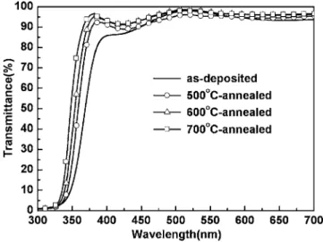
came the dominant factor reducing the responsivity. Figure 3 shows the typical light transmittance of the AZO films on sapphire before and after thermal annealing at different tem-peratures. In addition to the as-deposited samples, all an-nealed AZO samples exhibited high transparency共⬎90%兲 in the wavelength range of 400 nm to 700 nm. On the other hand, one can see that the transmittances were lower than 10% when the incident wavelength was shorter than 345 nm. The absorption band edge observed in the transmittance spectroscopy of AZO films was consistent with the short-wavelength cutoff shown in the spectral response of n -GaN / AZO PDs. Although the absorption band edges, all measuring around 370 nm, could shift to higher energy with an increase of annealing temperature, the improvement in transparency in ultraviolet 共UV兲 region was rather limited. Therefore, observed width of the spectral response was al-most the same even though thermal annealing process was applied to n-GaN / AZO PDs. Therefore, our study suggests that wider spectral response should be dominated by the thickness of AZO layer. Similar phenomenon is observed in a thin p-type layer of a p-i-n PD resulting in wider spectral response and higher peak responsivity, which occur due to absence of so-called ”optical dead space,” where carriers re-combine without being collected.16 Hence, both the low-resistivity and wide-band-gap TCO layers are useful in ex-panding the depletion region into the n-type i layer, thus resulting in a higher responsivity and wider spectral sponse. The study suggests that the width of spectral re-sponse can be manipulated by application of the AZO top contact layer with a different thickness.
Summarizing the findings, we should note that GaN Schottky barrier PDs featuring an AZO top contact layer were successfully fabricated. The research showed that spec-tral responsivity exhibited a narrow bandpass characteristic with a full width at half maximum of around 12 nm. More-over, the unbiased peak responsivity was estimated to be 0.12 A / W at 365 nm, corresponding to a quantum efficiency of 40%. In turn, low peak responsivity could be attributed to the absorption of the thick AZO top contact layer. Addition-ally, the dark currents of all samples including the as-deposited and the annealed samples showed almost the same order. Typically, all dark currents were well below 5 ⫻10−12A when reverse biases were below 5 V, thus imply-ing that present GaN Schottky barrier PDs with AZO top contact exhibit good thermal stability.
The authors would like to acknowledge the Center for Micro/Nano Technology Research, National Cheng Kung University, Tainan, Taiwan, for equipment access and tech-nical support and the financial support, from the National Science Council and Ministry of Economic Affairs from their Research Grant Nos. of 2118-E-218-010, NSC-94-2215-E-006-015, and MOEA-94-EC-17-A-07-S1-043.
1X. A. Cao, S. J. Pearton, G. Dang, A. P. Zhang, F. Ren, and J. M. Van Hove, Appl. Phys. Lett. 75, 4130共1999兲.
2Q. Z. Liu, L. S. Yu, S. S. Lau, J. M. Redwing, N. R. Perkins, and T. F. Kuech, Appl. Phys. Lett. 70, 1275共1997兲.
3L. Wang, M. I. Nathan, T.-H. Lim, M. A. Khan, and Q. Chen, Appl. Phys. Lett. 68, 1267共1996兲.
4C. T. Lee, Y. J. Lin, and D. S. Liu, Appl. Phys. Lett. 79, 2573共2001兲. 5J. Kyu Kim, H. W. Jang, C. M. Jeon, and J.-L. Lee, Appl. Phys. Lett. 81,
4655共2002兲.
6J. K. Sheu, Y. K. Su, G. C. Chi, M. J. Jou, and C. M. Chang, Appl. Phys. Lett. 72, 3317共1998兲.
7J. K. Sheu, M. L. Lee, and W. C. Lai, Appl. Phys. Lett. 86, 052103共2005兲 and references therein.
8C. J. Kao, J. K. Sheu, W. C. Lai, M. C. Chen, M. L. Lee, and G. C. Chi, Appl. Phys. Lett. 85, 1430共2004兲.
9S. J. Chang, M. L. Lee, J. K. Sheu, W. C. Lai, Y. K. Su, C. S. Chang, C. J. Kao, G. C. Chi, and J. M. Tsai, IEEE Electron Device Lett. 24, 212 共2003兲.
10N. Biyikli, I. Kimukin, B. Butun, O. Aytur, and E. Ozbay, IEEE J. Sel. Top. Quantum Electron. 10, 759共2004兲.
11J. K. Sheu, Y. K. Su, G. C. Chi, M. J. Jou, C. M. Chang, C. C. Liu, and W. C. Hung, J. Appl. Phys. 85, 1970共1999兲.
12M. L. Lee, J. K. Sheu, W. C. Lai, S. J. Chang, Y. K. Su, M. G. Chen, C. J. Kao, J. M. Tsai, and G. C. Chi, J. Appl. Phys. 94, 1753共2003兲. 13J. O. Song, K. K. Kim, S. J. Park, and T. Y. Seong, Appl. Phys. Lett. 83,
479共2003兲.
14V. Gupta and A. Mansingh, J. Appl. Phys. 80, 1063共1996兲.
15M. L. Lee, J. K. Sheu, W. C. Lai, S. J. Chang, Y. K. Su, M. G. Chen, C. J. Kao, J. M. Tsai, and G. C. Chi, Appl. Phys. Lett. 82, 2913共2003兲. 16D. J. H. Lambert, M. M. Wong, U. Chowdhury, C. Collins, T. Li, H. K. Kwon, B. S. Shelton, T. G. Zhu, J. C. Campbell, and R. D. Dupuis, Appl. Phys. Lett. 77, 1900共2000兲.
FIG. 3. Typical light transmittances of the AZO films deposited on sapphire before and after thermal annealing at different temperatures.
043506-3 Sheu et al. Appl. Phys. Lett. 88, 043506共2006兲