國
立
交
通
大
學
光電工程學系碩士班
碩
士
論
文
硼摻雜效應於超高密度矽量子點薄膜之研究
Boron Doping Effect on the Super-High Density Si Quantum
Dot Thin Films
研 究 生
:陳佑政
指導教授:李柏璁 教授
硼摻雜效應於超高密度矽量子點薄膜之研究
Boron Doping Effect on the Super-High Density Si Quantum
Dot Thin Films
研 究 生:陳佑政 Student:You-Jeng Chen
指導教授:李柏璁 Advisor:Prof. Po-Tsung Lee
國 立 交 通 大 學
光電工程學系碩士班
碩 士 論 文
A Thesis
Submitted to Department of photonics
College of Electrical Engineering and Computer Science National Chiao Tung University
in partial Fulfillment of the Requirements for the Degree of Master
in
Electro-Opticals Engineering September 1997
Hsinchu, Taiwan, Republic of China
i
硼摻雜效應於超高密度矽量子點薄膜之研究
研究生:陳佑政
指導教授:李柏璁 博士
國立交通大學光電工程學系碩士班
摘要
為了縮短矽量子點間距以提升載子穿隧機率,我們之前已提出並成功開發 以漸變矽過多氧化矽多層膜(Gradient Si-rich oxide multilayer, GSRO-ML)結構製 作出超高密度矽量子點薄膜。在此篇論文中,我們則針對硼摻雜效應與量子點 尺寸效應對於此超高密度矽量子點薄膜特性之影響做更進一步探討與研究。在 硼摻雜效應下,隨著硼濺鍍功率增加,我們觀察到高結晶率矽量子點保持與些 微縮小的能隙變化,而在硼濺鍍功率從 0 增加至 25W 時,由於有效活化硼摻雜 原子增加,可使薄膜電性與元件光伏特性皆有明顯提升,但當硼濺鍍功率高於 30W 時,則會受限於非有效活化硼摻雜原子增加與硼原子於界面過度擴散導致 薄膜與元件的整體效益皆明顯下降。然而,我們也驗證藉由插入一低硼摻雜濃 度的 GSRO-ML 可大幅改善此界面過度擴散的問題並有效提升元件效益。在量 子點尺寸效應下,藉由增加 GSRO-ML 的成核層厚度,從薄膜的光學吸收與元 件的量子效率響應譜圖皆清楚觀察到紅移現象,證實了矽量子點尺寸效應的貢 獻。因此,在此篇論文中,我們驗證了硼摻雜與量子點尺寸效應對矽量子點薄 膜特性的顯著影響,未來將針對薄膜厚度和硼摻雜濃度與分佈等關鍵因素做更 進一步的優化,以更提升元件工作效益。ii
Boron Doping Effect on the Super-High Density Si
Quantum Dot Thin Films
Student:You-Jeng Chen
Advisor:Dr. Po-Tsung Lee
Institute of Electro-Optical Engineering
National Chiao Tung University
Abstract
In order to further reduce quantum dot (QD) separation, we had proposed and successfully developed the gradient Si-rich oxide multilayer (GSRO-ML) structure for the super-high density Si QD thin films with larger carrier tunneling probability. In this study, we investigate the B-doping and QD size effects on the super-high density Si QD thin films by using a GSRO-ML structure. Under B-doping effect, the preserved high crystallinity of Si QDs and the slightly reduced Eg with increasing PB
are observed, besides, the electrical and PV properties are enhanced with increasing PB from 0 to 25W due to the increased active B-doped atoms but degraded at the
higher PB than 30 W due to the increased inactive B-doped atoms and the interfacial
over-diffusion of B-doped atoms. The decreased VOC with increasing PB due to the
interfacial over-diffusion is efficiently improved by inserting the lowly B-doped GSRO thin films as buffer layers. Under QD size effect, the red-shift effect is clearly confirmed in the absorption band edge and quantum efficiency response with
increasing NL thickness. Therefore, our results had demonstrated the feasibility and great potential for the higher efficiency Si-based solar cells integrating Si QDs by using a GSRO-ML structure.
iii
Acknowledgement
兩年的研究所生涯就要在這邊結束,在這期間不論是在實驗上或是生活上 都受到了很多身邊的人的幫助,沒有他們的幫助我不可能會這麼順利的完成我 的研究,所以我很感謝能夠讓我遇到這些老師、學長姐、同學、學弟妹。 首先是李柏璁教授,感謝教授在我的研究期間提供的幫助與建議以及平常 生活的關心,讓我覺得研究室充滿了親切的氛圍。接著要感謝郭光揚學長對於 我的研究提出的建議以及實驗上的探討,也持續的教導我關於量子點的知識, 沒有學長的幫忙我沒有辦法順利完成我的實驗。感謝林佳裕學長、黃品睿學姊、 劉權政學長在實驗上的幫助,大幅的減輕了在實驗上的負擔。感謝盧贊文學長、 蔡家揚學長、林品佐學長、張開浩學長對於我的生活的關照以及關心。感謝劉 權政學長、蔡為智學長、吳哲嶢學長在實驗室裡一起活動解悶。感謝朱恒沂小 朋友每次都在跟我互相吐槽,讓我在這段時間裡不會太無聊。感謝學弟張家瑞、 鐘坤達幫我負擔一些實驗減輕我的壓力。感謝學弟許澤恩、鄭聖諺陪我一起打 球運動。還要感謝那些實驗機台正常運作讓我能夠完成我的研究,感謝我在碩 士班期間遇到的所有同學,讓我的碩士生涯充滿回憶! 最後要感謝我的家人這麼的支持我,讓我完成我的碩士學位又沒有生活上 的顧慮,感謝我的爸媽、姊姊、妹妹,我愛你們! 陳佑政 2013 年 10 月 謹誌於 新竹交通大學 交映樓iv
Content
摘要 ... i Abstract ... ii Acknowledgement... iii Content ... iv List of Figures ... viList of Tables ... viii
CH.1 Introduction ... 1
1.1 Background of Solar Cells ... 1
1.2 Tandem Si-based Solar Cells ... 3
1.2.1 Energy Loss in Single Junction Solar Cells ... 3
1.2.2 Quantum Confinement Effect ... 5
1.2.3 Tandem Si-based SCs Integrating Si QD thin films ... 6
1.3 Paper Review ... 8
1.4 Motivation ... 12
CH.2 Fabrication of B-doped Si QD Thin Films ... 13
2.1 Substrate Clean ... 14
2.2 Deposition of Gradient Si-rich Oxide Multilayer (GSRO-ML) Thin Films ...15
2.2.1 Principle of Radio Frequency (RF) Magnetron Sputtering . 15 2.2.2 B-doped GSRO-ML Thin Film ... 16
2.3 Post-annealing Process ... 17
2.4 Thermal Oxide Layer Remove ... 17
2.5 Deposition of Electrode Layer ... 18
CH.3 Experimental Measurement ... 19
3.1 Raman Scattering Spectrum ... 19
3.2 Ultraviolet/Visible/Near-infrared (UV/VIS/NIR) Spectrum ... 21
3.3 Photoluminescence (PL) Spectrum ... 22
3.4 Current-Voltage (I-V) Curve and Hall Measurement ... 23
3.5 Quantum Efficiency (QE) Spectrum ... 23
3.6 Photoelectric Conversion Efficiency ... 24
CH.4 Result and Discussion ... 25
4.1 High Density Si QD Thin Films under Different B Sputtering Powers ... 25
4.1.1 Nano-crystalline Properties ... 25
v
4.1.3 Photoluminescence (PL) Properties ... 28
4.1.4 Electrical Properties ... 30
4.1.5 Photovoltaic (PV) Properties ... 32
4.1.6 Internal Quantum Efficiency (IQE) Spectra ... 34
4.2 Si QD Thin Films under Different Nucleation Layer (NL) Thickness ...35
4.2.1 Optical Absorption Properties ... 36
4.2.2 Internal Quantum Efficiency (IQE) Spectra ... 37
4.3 Si QD Thin Films under Different B-doped Distribution ... 38
4.3.1 PV Properties with and without Lowly B-doped GSRO-ML Thin Films Inserted ... 39
4.3.2 PV Properties under Different Inserted Pairs of Lowly B-doped GSRO-ML Thin Films ... 40
4.4 Summary ... 42
CH.5 Conclusion and Future Work ... 43
5.1 Conclusion ... 43
5.2 Future Work ... 44
vi
List of Figures
Fig. 1-1 Efficiency and cost projections for first- (I), second- (II), and third
generation (III) PV technologies [1]. ... 2
Fig. 1-2 Loss processes in a standard solar cell: non-absorption of below bandgap photons; lattice thermalization loss; and junction and contact voltage losses; recombination loss (radiative recombination is unavoidable). ... 3
Fig. 1-3 Illustration of 3-D time-independence Schrödinger's equation and boundary condition [3]. ... 5
Fig. 1- 4 (a) Illustration of Si QD embedded in materials with different QD size. (b) Experimental bandgaps of Si QDs embedded in SiO2 and SiNx from other groups [4]. ... 6
Fig. 1-5 Scheme of Si-based tandem solar cell [5]. ... 7
Fig. 1-6 (a) Illustration of p-Si QDs/n-Si heterojunction solar cell and representative TEM micrographs of the (b) as-deposited and (c) annealed [B-doped SiO1.0/SiO2]25 SL films at 1100◦C for 10 min. (d) Current–voltage (IV) characteristics under air mass 1.5 (AM 1.5G) illumination of 100 mW cm−2. ... 8
Fig. 1-7 Schematic of diode with self-aligned contacts. ... 9
Fig. 1-8 Measured (a) dark and (b) under a simulated 1-Sun illumination IV characteristics of a 2.2mm2 diode. ... 9
Fig. 1-9 (a) High-resolution TEM images of samples [SiO2/SRO]-ML and GSRO-ML. (b) The corresponding QD size distributions. ... 10
Fig. 1-10 Absorption spectra of samples GSRO-ML and [SiO2/SRO]-ML. Inset shows the corresponding Tauc plots for the indirect allowed transition. ... 10
Fig. 1-11 Dark I–V curves of samples GSRO-ML and [SiO2/SRO]-ML. Inset shows the corresponding light I–V curves under halogen lamp illumination. ... 11
Fig. 2-1 Fabrication process of Si QD thin films. ... 13
Fig. 2-2 Clean process chart of (a) Si wafer and (b) quartz substrates. ... 14
Fig. 2-3 Illustration of operation of magnetron sputtering deposition method. ... 15
Fig. 2-4 (a) Schematic diagram of varied sputtering power and (b) as-deposited GSRO-ML. ... 16
Fig. 2-5 Scheme of as-deposited and annealed Si QD thin films with GSRO-ML structure. ... 17
Fig. 2-6 Schemes of top electrodes of (a) square, (b) finger and (c) top electrode for Hall measurement... 18
Fig. 3-1 Diagram of Raman energy transition. ... 19 Fig. 3-2 Three components decomposd from Raman spectra of Si QD thin films [13].
vii
... 20
Fig. 3-3 Scheme of electronic transition. ... 22
Fig. 4-1 Raman spectra of the B-doped Si QD thin films under different PB. Inset shows the corresponding crystallinity of Si QDs. ... 26
Fig. 4-2 (a) Absorption coefficient spectra of the B-doped Si QD thin films under different PB and (b) the corresponding optical bandgaps. ... 27
Fig. 4-3 (a) PL spectra under different PB. ... 29
Fig. 4-4 Optical bandgaps obtained from quantum confinement effect for the Si QD thin films under different PB. ... 29
Fig. 4-5 (a) Hole concentration, mobility, and (b) conductivity of the Si QD thin films under different PB. ... 31
Fig. 4-6 (a) Illustration of the distribution of B-doped atoms in Si QD and the atomic bond structure for the (b) active and (c) inactive B atoms []. ... 31
Fig. 4-7 Light I-V curves of samples under different PB. ... 33
Fig. 4-8 Parameters of VOC, JSC, F.F., and η for samples under different PB. ... 33
Fig. 4-9 IQE spectra of samples under different PB. ... 34
Fig. 4-10 Scheme of fabrication process for the Si QD thin films under different NL thicknesses. ... 35
Fig. 4-11 (a) Absorption coefficient spectra of the Si QD thin films under different NL thickness and (b) the corresponding optical bandgap from Tauc plot. ... 36
Fig. 4-11 (a) Full and (b) short-wavelength ranged IQE spectra of samples under different NL thickness. ... 37
Fig. 4-12 Comparison of SIMS profiles for the as-deposited and annealed Si QD thin films fabricated by Eun-Chel Cho et al..[] ... 38
Fig. 4-13 Schematic diagram of the heavily and lowly B-doped GSRO-ML thin films on n-type Si substrate. ... 39
Fig. 4-14 Schematic diagram of sample B30 inserted by different pairs of B0 layers. ... 40
Fig. 4-15 PV parameters of VOC, JSC, F.F. and for sample B30 inserted by different pairs of B0 layers. ... 41
Fig. 4-16 Shunt resistance (Rsh) for sample B30 inserted by different pairs of B0 layers. ... 41
viii
List of Tables
Table 1-1 Theoretical efficiencies and corresponding bandgap combination
depending on the active cell layers [6]. ... 7
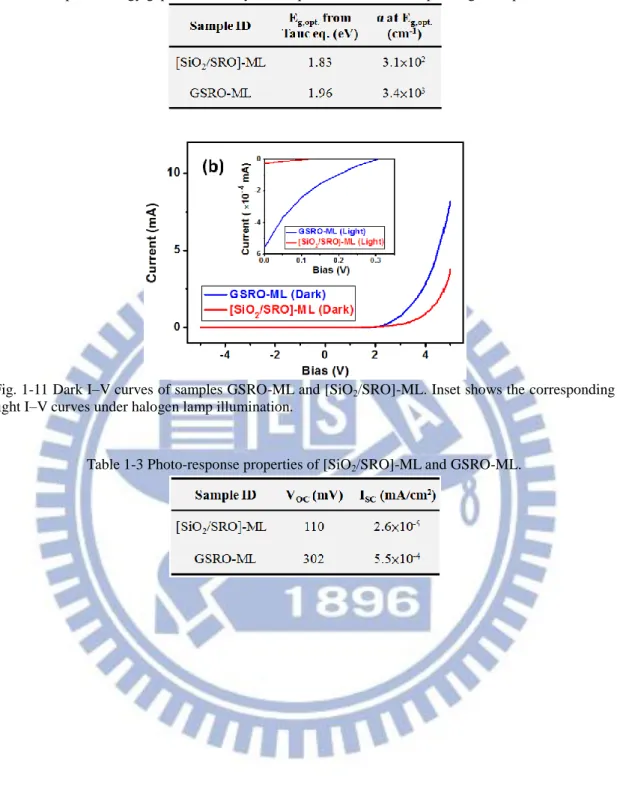
Table 1-2 Optical energy gap calculated by Tauc equation and the corresponding absorption coefficient. ... 11
Table 1-3 Photo-response properties of [SiO2/SRO]-ML and GSRO-ML. ... 11
Table 4-1 Parameters of the B-doped Si QD thin films under different PB. ... 25
Table 4-2 Absorption coefficients of different structures for Si materials []. ... 27
Table 4-3 VOC values of the heavily and heavily/lowly GSRO-ML thin films on n-Si substrates under 20 and 30 W of PB. ... 39
1
CH.1 Introduction
1.1
Background of Solar Cells
Energy shortage, global warming and population growth are the three main factors that affect people’s goals for sustainable development. In contemporary society, fossil fuels are the major world’s supply of energy source, and they are also the primary culprit behind climate change. Beside, the shortage in fossil fuel and increase of world energy consumption will lead to an energy crisis in the foreseeable future. These problems mentioned above lead us to find out the substitute energies, which generating energy from renewable sources are paramount for sustaining future energy supplies. Solar energy that converts light energy directly into electricity by the photovoltaic (PV) effect is among a number of promising renewable energy technology that is being pursued.
The solar cells can be classified into three generations as shown in Fig. 1-1. The first generation solar cells are silicon wafer-based solar cells which perform the high efficiency but high cost, like crystalline silicon (c-Si) bulk solar cell. For reducing the cost, second generation solar cells like amorphous silicon (a-Si) and organic cells have been developed. The cost of second generation solar cells is quiet cheaper than that of first generation solar cells. On the contrary, the efficiency of second generation solar cells is less than that of first generation solar cells. For achieving solar cells with high efficiency which is potential to be larger than efficiency limit of solar cells with single bandgap (33.7%) and low cost, the third generation solar cells such as polymer solar cells, nanocrystalline solar cells and multi-junction solar cells are being studied. Even if the third generation solar cell is superior to the others, they are still in research phase.
2
Fig. 1-1 Efficiency and cost projections for first- (I), second- (II), and third generation (III) PV technologies [1].
3
1.2
Tandem Si-based Solar Cells
1.2.1
Energy Loss in Single Junction Solar Cells
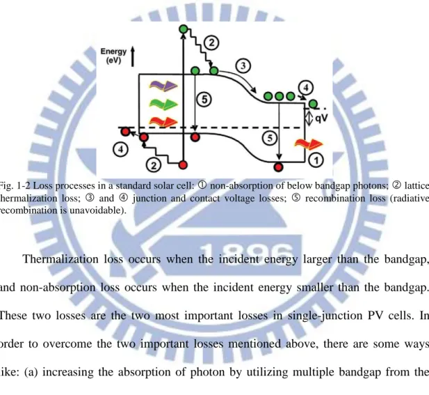
In the standard single junction solar cell, there exist five loss paths of energy, including junction loss, contact loss, recombination loss, non-absorption loss (low-energy loss) and thermalization loss (high-energy loss) as shown in Fig. 1-2 [2].
Fig. 1-2 Loss processes in a standard solar cell: non-absorption of below bandgap photons; lattice thermalization loss; and junction and contact voltage losses; recombination loss (radiative recombination is unavoidable).
Thermalization loss occurs when the incident energy larger than the bandgap, and non-absorption loss occurs when the incident energy smaller than the bandgap. These two losses are the two most important losses in single-junction PV cells. In order to overcome the two important losses mentioned above, there are some ways like: (a) increasing the absorption of photon by utilizing multiple bandgap from the wide-range spectrum; (b) capturing carrier before thermalization; (c) multiple carrier pair generation per high energy photon or single carrier pair generation with multiple low energy photons. Among these, tandem solar cells, stacking sub-cells from large to small bandgap in turn, are the reliable structure to achieve a high efficiency SC. There are several nanostructured cell proposals that aim at higher efficiency. The nanocrystalline Si can be made less than 7 nm in diameter and behave as quantum
4
dots (QDs), e.g. bandgap control with nanocrystal size, very fast optical transition, and multiple carrier generation, owing to the three-dimensional quantum confinement of carrier [3]. Nanocrystalline Si embedded in dielectric material cascaded with silicon-based solar cells is one of the proposed solar cell structures to achieve super high conversion efficiency due to its ability in energy bandgap engineering.
5
1.2.2
Quantum Confinement Effect
Behavior of particle waves confined in an infinite quantum well can be explained by three-dimensional (3-D) time-dependence Schrödinger's equation expressed as
We can obtain that allowance energy states are discrete and they dependent on the width of the quantum well. The phenomenon comes from the quantum confinement effect. For particle-waves confined in nanoparticles covered in materials with finite barrier height, similar energy states can be obtained, as expressed by Eq. (1-2)
Where nx, ny, nz are integers and equal to 1 for the ground state square box.
Discrete energy levels depend on the dimension of nanoparticles and barrier height between nanoparticles and materials which cover around them. Fig. 1-4 shows the wave functions of different nanoparticles sizes with a fixed barrier height and those of different barrier with a fixed nanoparticle size. As a result, we can control effective bandgap by tuning the QD's size and changing the matrix material.
6
1.2.3
Tandem Si-based SCs Integrating Si QD thin films
According to quantum theory, when the QD's size is approached to nanoscale, the quantum confinement effect will occur. It will relax the K-space conservation requirement and transform the Si bandgap properties from indirect to quasi-direct and modify the effect bandgap of Si. Fig. 1-4(a) shows the Si QDs embedding in a wide bandgap material can lead to a highly-tunable effective bandgap, and Fig. 1-4(b) shows the effective bandgap of Si QD can be widely modified by tuning the QD's size in SiO2 or Si3N4 matrix. This indicated that it's feasible to achieve the wide bandgap
which is larger than c-Si and a-Si material by using Si QD thin films. Hence, we can integrate Si QDs into Si-based solar cells to reduce energy losses from mismatch bandgap.
(a) (b)
Fig. 1- 4 (a) Illustration of Si QD embedded in materials with different QD size. (b) Experimental bandgaps of Si QDs embedded in SiO2 and SiNx from other groups [5].
In order to achieve high efficiency and low cost solar cell, the third generation solar cells have been studied. One of the promising candidates is the tandem solar cell using Si QD thin films as shown in Fig. 1-5 [6]. The concept of the tandem solar cell is stacking different bandgap of solar cells from large to small ones for the absorbing different energy of photons. The uppermost cell has the largest bandgap and lets the
7
photon which energy less than its bandgap passing through to lower bandgap cells underneath.
Tandem solar cell using Si QD thin films stacking materials with different energy bandgap can utilize the wide solar spectrum more effectively. Table 1-1 shows the best bandgap combinations under different numbers and their theoretical efficiencies [7].
Fig. 1-5 Scheme of Si-based tandem solar cell [6].
Table 1-1 Theoretical efficiencies and corresponding bandgap combination depending on the active cell layers [7].
8
1.3
Paper Review
Recently, the fabrication and study of nanostructure silicon systems have been largely developed due to the potential for optoelectronic applications. Most of the studies were devoted to QD structures and to multilayered configurations for the fabrication of optoelectronic devices. The QD structure consists in the elaboration of composite materials made of nanocrystalline Si embedded in a transparent and insulating matrix (SiO2). They are commonly fabricated by ion implantation of Si+ [8,
9], plasma enhanced chemical vapor deposition [10, 11] or by magnetron sputtering [12, 13, 14], and they have commonly been deposited by a [silicon dioxide/silicon-rich oxide] multilayer ([SiO2/SRO]-ML) structure.
Since the Si QD thin films integrated in PV devices, it shows the feasibility and great potential. For example, K. J. Kim et al. proposed integrating Si QD thin films with Si-based SCs with high efficiency in 2011 [15]. In this study, they achieved the heavily B-doped Si QD thin films by co-sputtering B with Si and SiO2 targets, and
they demonstrated a p-type Si QD solar cell with a high energy conversion efficiency of 13.4% was realized from a [B-doped SiO1.0 (2nm)/SiO2 (2nm)] 25-period
superlattices film (Fig. 1-6 (c)) with a B doping concentration of 4×10²⁰ atoms cm-3.
(a) (b) (c) (d)
Fig. 1-6 (a) Illustration of p-Si QDs/n-Si heterojunction solar cell and representative TEM micrographs of the (b) as-deposited and (c) annealed [B-doped SiO1.0/SiO2]25 SL films at 1100
◦
C for 10 min. (d) Current–voltage (IV) characteristics under air mass 1.5 (AM 1.5G) illumination of 100 mW cm−2.
9
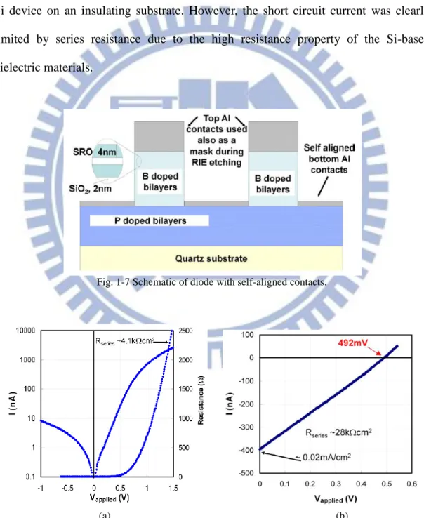
In 2012, the all Si QD thin film solar cell had been fabricated on a quartz substrate by I. Perez-Wurfl et al. [16]. They fabricated p-i-n diodes (Fig. 1-7) by sputtering alternating layers of SiO2 and SRO with in situ boron for p-type and
phosphorus for n-type doping. The dark and illuminated I–V characteristics of the fabricated diodes showed a rectifying behavior with an open circuit voltage (VOC) of
492 mV (Fig. 1-8(b)), and this is the largest VOC reported to date for nanocrystalline
Si device on an insulating substrate. However, the short circuit current was clearly limited by series resistance due to the high resistance property of the Si-based dielectric materials.
Fig. 1-7 Schematic of diode with self-aligned contacts.
(a) (b)
Fig. 1-8 Measured (a) dark and (b) under a simulated 1-Sun illumination IV characteristics of a 2.2mm2 diode.
10
In order to improve the carrier transportation efficiency in Si QD thin films, we had proposed a new gradient Si-rich oxide multilayer (GSRO-ML) deposition structure in 2013 [17]. Without using SiO2 barrier layer, the Si QD thin film using a
GSRO-ML deposition structure showed excellent capabilities, not only a higher QD density but also a good QD size control, as shown in Fig. 1-9. Compared with a [SiO2/SRO]-ML structure, sample GSRO-ML has improved carrier transport
efficiency and a larger optical absorption coefficient resulting from the formation of QDs with higher density, as shown in Fig. 1-10 and Table 1-2. The enhancements on electro-optical properties in sample GSRO-ML are also obtained, as shown in Fig. 1-11 and Table 1-3. However, the PV properties in this study are still not high enough for achieving high-efficiency solar cells. It can be improved by other ways with using GSRO-ML deposition structure.
(a) (b)
Fig. 1-9 (a) High-resolution TEM images of samples [SiO2/SRO]-ML and GSRO-ML. (b) The corresponding QD size distributions.
Fig. 1-10 Absorption spectra of samples GSRO-ML and [SiO2/SRO]-ML. Inset shows the corresponding Tauc plots for the indirect allowed transition.
11
Table 1-2 Optical energy gap calculated by Tauc equation and the corresponding absorption coefficient.
Fig. 1-11 Dark I–V curves of samples GSRO-ML and [SiO2/SRO]-ML. Inset shows the corresponding light I–V curves under halogen lamp illumination.
12
1.4
Motivation
The efficiency of Si QD solar cell is not high enough even using the GSRO-ML structure. According to studies, higher B doping will move the Fermi level to the valence band, thereby increasing the potential difference at the p-n heterojunction of p-type QDs/ n-type Si wafer. Hence, in order to improve the PV characteristic of Si QD thin film, achieving the heavily doping in Si nanocrystals is necessary.
In this study, we proposed the B doped Si QD thin films with GSRO-ML structure. Here we expect the built-in electrical field and carrier concentration can be enhanced effectively by heavily B doping in Si QD. We will discuss the characteristic about crystalline, optical, electrical and PV properties in this thesis.
13
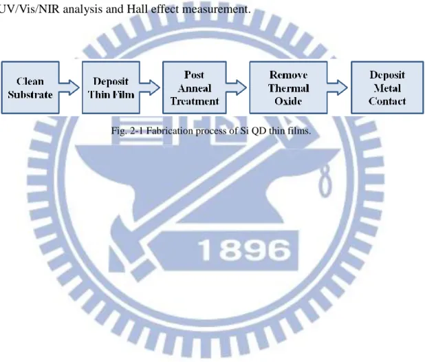
CH.2 Fabrication of B-doped Si QD Thin Films
In this chapter, we introduce the fabrication process of our samples. The process is shown in Fig. 2-1. In this study, we use two different substrates to analysis the characterization of Si QD thin films. One is n-type Si(100) wafer for photoluminescence (PL) analysis, X-ray diffraction, quantum efficiency (QE) and electrical measurement. The other one is quartz for Raman scattering analysis, UV/Vis/NIR analysis and Hall effect measurement.
14
2.1
Substrate Clean
The cleaning procedures for substrate are shown as Fig. 2-2. Si wafers are cleaned by standard RCA cleaning as shown in Fig. 2-2(a). The main purpose of RCA cleaning is to remove the particles, organic contaminates and native oxide on the wafer. And we clean quartz in acetone and ethanol for 10min by ultrasonic cleaner to remove organic contaminates on the quartz surface. The process is shown in Fig. 2-2(b).
(a) (b) Fig. 2-2 Clean process chart of (a) Si wafer and (b) quartz substrates.
15
2.2
Deposition of Gradient Si-rich Oxide Multilayer
(GSRO-ML) Thin Films
2.2.1
Principle of Radio Frequency (RF) Magnetron Sputtering
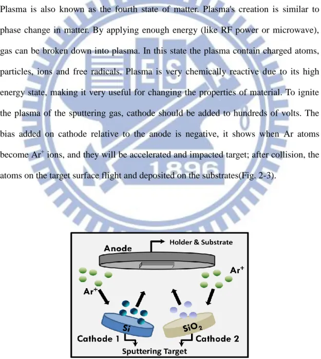
The basic principle of sputtering is to accelerate the ion to bombard the target surface, after ion and atomic in solid surface exchange the momentum, atoms will spill from the solid surface, this phenomenon called sputtering.
Sputtering mainly depends on the state of the plasma ions and free radicals. Plasma is also known as the fourth state of matter. Plasma's creation is similar to phase change in matter. By applying enough energy (like RF power or microwave), gas can be broken down into plasma. In this state the plasma contain charged atoms, particles, ions and free radicals. Plasma is very chemically reactive due to its high energy state, making it very useful for changing the properties of material. To ignite the plasma of the sputtering gas, cathode should be added to hundreds of volts. The bias added on cathode relative to the anode is negative, it shows when Ar atoms become Ar+ ions, and they will be accelerated and impacted target; after collision, the atoms on the target surface flight and deposited on the substrates(Fig. 2-3).
16
2.2.2
B-doped GSRO-ML Thin Film
To deposit B-doped GSRO-ML thin films, we use the sputtering system which is co-sputtering lowly B-doped Si, B and SiO2 targets alternatively. During deposition,
we modulate Si sputtering power from 30 to 110 W and back to 30 W with rate of 1W per second for 20 periods while the SiO2 sputtering power are fixed at 30 W. In each
center region, we replace the SiO2 by injecting the oxygen gas, and co-sputter the Si
and B target with the Si sputtering power are held at 110 W and fixed B sputtering power at 0, 10, 20, 30, 40 and 50W respectively to form 1nm B-doped highly Si-rich oxide layer as nucleation layer. The schematic diagram is shown in Fig. 2-4(a). By this method, we obtain a periodical GSRO distribution (Fig. 2-4(b)).
(a) (b)
17
2.3
Post-annealing Process
After deposition, the GSRO-ML thin films were treated with high temperature annealing process to precipitate Si atoms due to phase separation of Si and SiO2
according to the following equation:
Here we annealed all samples in a nitrogen atmosphere at 1100°C for 1hour in a quartz-tube furnace to form Si QDs.
Fig. 2-5 Scheme of as-deposited and annealed Si QD thin films with GSRO-ML structure.
2.4
Thermal Oxide Layer Remove
After annealing process, a thin thermal oxide layer was formed on the top and bottom of samples due to residual oxygen in the furnace. The thermal oxide layers make an influence on the collection efficiency of photo-generated carriers. In order to reduce the influence of the thermal oxide layers, we remove top side oxide layer by CHF3:O2 reactive ion etching (RIE) and bottom oxide layer by buffered oxide etch
18
2.5
Deposition of Electrode Layer
To measure the electrical properties, the contact electrodes were deposited on sample by thermal evaporation coater at the final process. We deposited Al layers on both top and bottom sides to form ohmic contact. The top electrodes are designed to square for the current-voltage measurement and finger for the efficiency measurement by solar simulator, as shown in Fig. 2-6 (a) and (b). The sample for Hall measurement was deposited only on top side, as shown in Fig. 2-6 (c). After the growth of Al electrode, the devices were heated at 200°C for 20 minutes to improve the contact properties at the interface of QD layers/electrodes.
(a) (b) (c)
19
CH.3 Experimental Measurement
3.1
Raman Scattering Spectrum
Confocal-Raman microscope is a powerful characterization technique to study materials vibration modes in a material. It is based on the Raman Effect [18], which is a form of light scattering; a photon excites the molecule from the ground state to a virtual energy state. When the molecule relaxes it to emit a photon, it returns to a different rotation or vibration state. The energy difference between the original state and the new state leads to a shift in the emitted photon's frequency away from the excitation wavelength. If the final vibrational state of the molecule is more energetic than the initial state, then the emitted photon will be shifted to a lower frequency in order to remain the balanced energy of the system. This shift in frequency is designated as a Stokes shift. If the vibration state is less energetic than the initial state, then the emitted photon will be shifted to a higher frequency, and this is designated as an Antie-Stokes shift. Raman scattering is an example of inelastic scattering because of the energy transfers between the photons and the molecules during their interaction. Fig. 3-1 shows the diagram of Raman energy transition.
20
We analyzed the samples by high-resolution confocal-Raman microscope (HORIBA LabRAM HR Raman Microscope), and used a 488-nm diode-pumped solid-state laser. The illuminated spot size is about 10um in diameter and the power of laser is about 7mW. Si substrate was used to calibrate the crystalline Si signal at 520cm-1 before measuring our samples.
Generally, three peaks can be detected in Si QD thin films, including amorphous phase (~480cm-1), intermediate phase (500~510cm-1) and crystalline phase (510~520cm-1), as shown in Fig. 3-2 [13]. The crystallinity (χc) can be estimated by
the following equation:
χ
where Ic, Ii and Ia are the intensity of crystalline, intermediate and amorphous phases
respectively.
21
3.2
Ultraviolet/Visible/Near-infrared (UV/VIS/NIR)
Spectrum
We used UV/VIS/NIR spectrophotometer (Hitachi U-4100, Japan) to measure the transmittance (T) and reflectance (R) of Si QD thin films, and calculate the absorbance (A) by
Thus, we can understand the optical properties of the thin films. And, the absorption coefficient ( ) can be obtained by the following relation:
where t represents the thickness of thin films. The optical bandgap (Eg,opt) of the thin
films are determined by the intercept of linear part of the absorption edge to =0 in the relationship as tauc's equation :
where h is Plank's constant, is the frequency of the radiation, and B is the edge width parameter [20]. The value of is dependent on the Eg,opt behavior, =1/2 for
22
3.3
Photoluminescence (PL) Spectrum
PL spectroscopy is a contactless, nondestructive method of probing the electrical structure of materials. Light is incident directly onto samples where it is absorbed and imparts excess energy into the material in a process called photo-excitation as shown in Fig. 3-3.
Fig. 3-3 Scheme of electronic transition.
The samples were analyzed by micro-PL measured on high-resolution Raman microscope (HORIBA LabRAM HR Raman Microscope). We used a laser on diode-pumped solid-state (DPSS) with a 488nm wavelength. The illuminated spot size is about 10um in diameter and the power of laser is about 7mW. Si substrate is used to calibrate the laser signal at 488nm before PL spectroscopy measurement. All PL spectra were measured at room temperature.
23
3.4
Current-Voltage (I-V) Curve and Hall Measurement
The electrical properties of Si QD thin films can be understood by I-V characteristics and Hall measurement. In addition, we can use the I-V characteristics to estimate the vertical resistivity from the linear trend in the high bias region. We can calculate the resistivity by combining the resistance as equation:
where is the resistivity, A is the cross-sectional area and L is the length. The cross-sectional area can be decomposed into the width W and the thickness t. The I-V curves in this study were measured by the E5270B 8 slot precision measurement mainframe (Agilent Technologies) and a halogen lamp illumination with power density of 3mW/cm2 was applied to photo-response measurements. The carrier concentration, mobility and resistivity were measured by the Hall effect measurement system (Swin HALL8800).
3.5
Quantum Efficiency (QE) Spectrum
QE measurement is a standard method to observe the percentage of incident photon converted to electron. We measured the external quantum efficiency (EQE) and reflectance (R), and calculated the internal quantum efficiency (IQE) by EQE and R. The samples in this study were measured by the solar cell quantum efficiency measurement system (Titan Electro-Optics, Hitachi QE-3000).
24
3.6
Photoelectric Conversion Efficiency
To confirm the PV properties, the standard measurement of sample under illumination is necessary. In this study, the samples with finger electrode for PV properties were measured by the solar simulator measurement system (Newport, Solar Simulator 91192A). To define the illuminated area, we measured the samples with covering a mask which have a 0.2cm2 empty area equal to the finger electrode area.
25
CH.4 Result and Discussion
4.1
High Density Si QD Thin Films under Different B
Sputtering Powers
In section 4-1, we discuss the high density Si QD thin films under different B sputtering powers (PB) from 0 to 50W by using a GSRO-ML deposition structure. The
parameters of the B-doped Si QD thin films under different PB are listed in Table 4-1.
The nano-structural, optical, electrical, and PV properties are investigated to understand the characteristics of the B-doped high density Si QD thin films.
Table 4-1 Parameters of the B-doped Si QD thin films under different PB.
4.1.1 Nano-crystalline Properties
Raman spectra, a well-known technique for the examinations of nano-crystalline properties of Si QDs, are performed. Generally, the signals can be decomposed into three components, including amorphous- (a-), intermediate- (i-) and crystalline- (c-) Si phases and the crystallinity of Si (fc-Si) is obtained by the following equation [19]:
where Inc, Ii and Ia are the integrated intensity of nc-, i- and a-Si phases respectively.
The higher fc-Si means the better crystal quality of Si QDs formed. Hence, to
investigate the nano-crystalline properties of Si QDs affected by the B-doped concentration, Raman spectra of the Si QD thin films under different PB are measured,
26
as shown in Fig. 4-1, and its inset shows the corresponding fc-Si. The close and high
(~75%) fc-Si of Si QDs under different PB means the B-doped concentration has no
significant influence on the crystal quality. Therefore, the high crystallinity for the Si QD thin films can be well maintained under the heavily B-doped concentration by using a GSRO-ML structure.
Fig. 4-1 Raman spectra of the B-doped Si QD thin films under different PB. Inset shows the corresponding crystallinity of Si QDs.
4.1.2 Optical Absorption Properties
To investigate the optical absorption properties of the B-doped Si QD thin films, the absorption coefficient (α) spectra and the corresponding optical bandgaps (Eg,opt)
obtained from Tauc plot for the Si QD thin films under different PB are examined, as
shown in Fig. 4-2. The red-shift effect on the absorption edge and the corresponding Eg,opt is observed while increasing the PB, which may be contributed from the effective
doping state due to the B-doped effect [21]. The α values at Eg,opt for the Si QD thin
films under different PB can be kept at ~2×103 cm-1, which is significantly larger α
27
material, as shown in Table 4-2. Hence, our results indicate that the higher B-doped concentration in the Si QD thin films using a GSRO-ML structure can lead to the slightly lower Eg,opt while the large α values are maintained.
(a) (b)
Fig. 4-2 (a) Absorption coefficient spectra of the B-doped Si QD thin films under different PB and (b) the corresponding optical bandgaps.
28
4.1.3 Photoluminescence (PL) Properties
In addition to optical absorption, the PL emission properties are also a commonly-used method to understand the characteristics of the Si QD thin films. According to literatures, the main PL emission of the Si QD thin films can be attributed to three recombination mechanisms, including the yellow emission from the defect states inside SiO2 matrix (PLD-SiO2) [23, 24], the near-infrared emission from
the interface states at the interfacial region between QDs and matrix (PLD-interface) [25,
26], the tunable visible emission from the quantum confinement (PLQC) effect inside
QDs [3, 27]. Fig. 4-3 shows the PL spectra of the Si QD thin films under different PB
and the curve-fitting result for sample B0. In our previous work, it had been demonstrated that more photo-generated carriers can transport through QDs rather than recombine inside QDs and matrix by using a GSRO-ML [17], hence, a lower PL intensity from QC effect is a reasonable result. In Fig. 4-3(a), the significantly decreased PL intensity by increasing PB from 0 to 20W is observed, which may due to
more nonradiative Auger recombination processes via three-holes interaction contributed from more efficient B-doped atoms [28-31]. However, the overall PL intensity is clearly increased by the higher PLD-SiO2 intensity with increasing PB when
PB is higher than 20W, it means the higher PB than 20W will produce more excess B
atoms and lead to more defects form in SiO2 matrix, and the over-high defect density
will degrade the carrier transport efficiency in the Si QD thin films. Fig. 4-4 also shows the corresponding Eg from QC effect for the Si QD thin films under different
PB, the decreased Eg with increasing PB clearly agrees with the results from optical
absorption properties, which may due to the effective doping state due to the B-doped effect [21]. Therefore, it represents the B-doped concentration can significantly influence the Eg of the Si QD thin films.
29 (a)
Fig. 4-3 (a) PL spectra under different PB.
Fig. 4-4 Optical bandgaps obtained from quantum confinement effect for the Si QD thin films under different PB.
30
4.1.4 Electrical Properties
In order to understand the electrical properties, the Si QD thin films deposited on quartz substrates under different PB were measured by Hall effect measurement, the
hole concentration, mobility, and conductivity were obtained and shown as Fig. 4-5. From Fig. 4-5 (a), the hole concentration is increased with increasing PB from 10 to
25 W and saturated at the higher PB, and the mobility is increased with increasing PB
from 10 to 15 W and saturated at 15 to 25 W then but obviously decreased at the higher PB. According to literatures, there are two possibilities for the B-doped atoms
in the Si QD thin films; one is the electrically active B atoms located inside Si QDs, the other one is the electrically inactive B atoms located at SiO2/Si QDs interface and
SiO2 matrix, as shown in Fig. 4-6 [15]. The excess B-doped atoms will diffuse into
SiO2/Si QDs interface and SiO2 matrix and cause the inactive B atoms, which are the
ineffective doping result for the holes contribution. Besides, the inactive B atoms will also induce more defects at the interface and inside the matrix and decrease the mobility due to the larger scattering effect. Hence, the variation of hole concentration, observed in Fig. 4-5(a), indicates that the amount of active B atoms is increased with increasing PB from 10 to 25 W and saturated at the higher PB, and the decreased
mobility when PB higher than25 W means the excess inactive B atoms produced.
Fig. 4-5(b) also shows the conductivity of the Si QD thin films under different PB.
The conductivity for samples with PB of from 10 to 50W were obtained from Hall
effect measurements, and that for sample B0 is calculated from the slope of the lateral I-V curve due to the larger resistance. The conductivity is largely increased from 0 to 15 W and saturated from 15 to 25 W, then decreased at the higher PB, which well
31
atoms are increased with increasing PB and saturated at 25 W, and the inactive B
atoms will be largely increased when PB is higher than 25 W. Therefore, the results
represent the B-doped concentration has the great effect on the electrical properties of the Si QD thin films, and a suitable doping concentration is required for the better electrical properties.
(a) (b)
Fig. 4-5 (a) Hole concentration, mobility, and (b) conductivity of the Si QD thin films under different PB.
(a) (b) (c)
Fig. 4-6 (a) Illustration of the distribution of B-doped atoms in Si QD and the atomic bond structure for the (b) active and (c) inactive B atoms [15].
32
4.1.5 Photovoltaic (PV) Properties
To understand the B-doping effect on PV properties, the light I-V curves of the Si QD thin films on n-Si substrates under different PB were measured under air-mass
1.5 global (AM 1.5G) illumination, as shown in Fig. 4-7, and Fig. 4-8 summarizes the corresponding parameters of open-circuit voltage (VOC), short-circuit current density
(JSC), fill factor (F.F.), and conversion efficiency (η). The VOC values are slightly
reduced with increasing PB from 10 to 25 W and further decreased at higher PB than
25 W. The JSC and F.F. values are obviously increased with increasing PB from 10 to
25 W but decreased at higher PB. Based on the variations on VOC, JSC, and F.F., the η
reveals the optimized value of 4.37 % at 25W of PB. According to references, the
doped atoms over-diffusing into Si substrates have been observed in the heavily doped Si QD thin films after annealing [32]. Hence, the decreased VOC while
increasing PB is considered as the degraded built-in electric field due to the
over-diffusion production of the excess B-doped atoms. The variations of JSC and F.F.
under different PB well agree with the films’ conductivity, which are increased with
increasing PB from 10 to 25W and decreased at higher PB, it means a suitable B-doped
concentration can efficiently improve the conductivity of the Si QD thin films, and then, lead to the enhanced JSC and F.F.. From these results, it represents that the
optimized B-doped concentration for the Si QD thin films can be obtained at 25 W of PB, and a higher PB than 25 W will cause the degraded PV properties due to the
33
Fig. 4-7 Light I-V curves of samples under different PB.
(a) (b)
(c) (d) Fig. 4-8 Parameters of VOC, JSC, F.F., and η for samples under different PB.
34
4.1.6 Internal Quantum Efficiency (IQE) Spectra
To confirm the photoresponse properties, samples under different PB were
characterized by internal quantum efficiency (IQE) spectra, as shown in Fig. 4-9. The IQE is largely increased from 10 to 20W but decreased from 20 to 30W. From our above results, it indicates the increased IQE from 10 to 20 W is contributed from the improved film’s electrical properties, and the decreased IQE from 20 to 30 W is due to the interfacial over-diffusion and excess inactive B atoms. Hence, we demonstrate the obviously B-doping effect on the super-high density Si QD thin films by using a GSRO-ML structure and tuning the B-doped concentration.
35
4.2
Si QD Thin Films under Different Nucleation Layer
(NL) Thickness
In order to investigate the QD size effect, we fabricated the Si QD thin films with different QD size by tuning the nucleation layer (NL) thickness for 1, 2, and 3 nm in a GSRO-ML structure, shown as Fig. 4-10. The PB was fixed at 20 W in these three
samples. After deposition, these samples were also annealed at 1100°C for 1hour.
36
4.2.1 Optical Absorption Properties
To confirm the QD size effect on optical absorption properties, the absorption coefficient spectra of the Si QD thin films under different NL thickness were examined, as shown in Fig. 4-11(a). From Fig. 4-11(a), we observe the red-shift effect of absorption band edge as increasing the NL thickness, and the reduced Eg,opt
obtained from Tauc plot with increasing NL thickness is also examined shown as Fig. 4-11(b). Hence, it represents the Eg of the Si QD thin films can be efficiently modified
by tuning the NL thickness.
(a) (b)
Fig. 4-11 (a) Absorption coefficient spectra of the Si QD thin films under different NL thickness and (b) the corresponding optical bandgap from Tauc plot.
37
4.2.2 Internal Quantum Efficiency (IQE) Spectra
To understand the QD size effect on photoresponse properties, the Si QD thin films under different NL thickness were characterized by IQE spectra measurements, as shown in Fig. 4-11. The red-shift IQE response in the short-wavelength range is clearly observed by increasing the NL thickness, which agrees with the results from optical absorption properties. It means the red-shift IQE response is caused by the reduced Eg due to the increased QD size from the increased NL thickness. Therefore,
we demonstrate the Eg can be efficiently modified by tuning the NL thickness in a
GSRO-ML structure, and the corresponding photoresponse from QD size effect can also be well achieved.
(a) (b)
Fig. 4-11 (a) Full and (b) short-wavelength ranged IQE spectra of samples under different NL thickness.
38
4.3
Si QD Thin Films under Different B-doped
Distribution
In section 4.1, we clearly observe the decreased VOC may due to the degraded
built-in electric field caused by the interfacial over-diffusion of B-doped atoms. According to references, the excess doped atoms diffusing into Si substrates had been observed in the heavily doped Si QD thin films by using a [SiO2/SRO]-ML structure
after annealing by Eun-Chel Cho et al., as shown in Fig. 4-12 [32]. Since the SiO2
barrier layer in a [SiO2/SRO]-ML structure can efficiently prevent the over-diffusion
from the doped atoms, more obvious diffusion from the heavily doped atoms in the Si QD thin films may occur by using a GSRO-ML structure. However, it could be efficiently resolved by inserting the lowly doped Si QD thin films as the buffer layers. Hence, in order to improve the cell’s performances, we propose to insert the lowly B-doped GSRO-ML thin films between the heavily B-doped GSRO-ML thin films and Si substrates to resolve the interfacial over-diffusion from B-doped atoms.
Fig. 4-12 Comparison of SIMS profiles for the as-deposited and annealed Si QD thin films fabricated by Eun-Chel Cho et al..[32]
39
4.3.1 PV Properties with and without Lowly B-doped
GSRO-ML Thin Films Inserted
In section 4.3.1, in order to investigate the influences from the interfacial over-diffusion of B-doped atoms, we fabricated the heavily (40 pairs) and heavily (20 pairs) / lowly (20 pairs) B-doped GSRO-ML thin films on n-type Si substrates shown as Fig. 4-13. The VOC values of samples with and without the lowly
GSRO-ML thin films inserted under 20 and 30 W of PB are shown in Table 4-3. The
VOC values of samples with B0 layers inserted are significantly higher than those of
samples without B0 layers inserted, besides, the increased VOC in sample B30 with
higher B-doped concentration is larger than that in sample B20 with lower B-doped concentration. Therefore, it represents the Ebuilt-in can be efficiently enhanced by
inserting the lowly B-doped GSRO-ML thin films owing to the improved interfacial over-diffusion.
Fig. 4-13 Schematic diagram of the heavily and lowly B-doped GSRO-ML thin films on n-type Si substrate.
Table 4-3 VOC values of the heavily and heavily/lowly GSRO-ML thin films on n-Si substrates under 20 and 30 W of PB.
40
4.3.2 PV Properties under Different Inserted Pairs of
Lowly B-doped GSRO-ML Thin Films
To further confirm the interfacial over-diffusion, sample B30 with B0 layers inserted from 0 to 20 pairs were fabricated and examined, as shown in Fig. 4-14. The PV properties of sample B30 under different inserted pairs of B0 are shown in Fig. 4-15. The VOC and F.F. of samples reveal the same tendency and the optimized values
at 10 pairs inserted. From the corresponding shunt resistances (Rsh), as shown in Fig.
4-16, it clearly indicates the increased VOC and F.F. are mainly contributed from the
better quality in the junction region owing to the improved interfacial over-diffusion. The lower cell’s performances of sample B30 inserted by 20 pairs of B0 may be caused by more undiffused B0 layers, which have poor film’s conductivity, after annealing. Fig 4-15(d) shows the same tendency of with those of VOC and F.F.
under different B0 layers inserted, and the is obviously enhanced from 1.7 to 3.9 % by inserting the B0 layers from 0 to 10 pairs. The significant enhancements on cell’s performances also demonstrate the interfacial over-diffusion can be efficiently improved by inserting the lowly B-doped GSRO-ML thin films with suitable thickness.
41
(a) (b)
(c) (d)
Fig. 4-15 PV parameters of VOC, JSC, F.F. and for sample B30 inserted by different pairs of B0 layers.
42
4.4
Summary
In chapter 4, we had successfully fabricated the heavily B-doped Si QD thin films by co-sputtering Si, SiO2, and B targets. In our results, the high crystallinity of
Si QD is maintained in the super-high density Si QD thin films under different PB,
and the slightly reduced Eg with increasing PB is observed from optical absorption
and PLQD emission. The electrical properties of the B-doped Si QD thin films are
largely improved from 0 to 25 W of PB due to the increased active B-doped atoms,
but significantly degraded at the higher PB than 30 W due to the increased inactive
B-doped atoms and/or the induced defects in SiO2 matrix. The better electrical
properties of the B-doped Si QD thin films can obviously enhance the JSC and F.F. of
cell’s performances, but the VOC decreased with increasing PB is observed due to the
degraded Ebuilt-in caused by the interfacial over-diffusion of B-doped atoms after
annealing. However, we also demonstrate the VOC and can be efficiently enhanced
by inserting the lowly B-doped Si QD thin films with suitable pairs as buffer layers during annealing. Therefore, the better cell’s performances can be expected by optimizing the concentration and distribution of B-doped atoms by using a GSRO-ML structure.
43
CH.5 Conclusion and Future Work
5.1
Conclusion
In this study, in order to obtain the better PV properties, the heavily B-doped super-high density Si QD thin films using a GSRO-ML structure have been proposed and fabricated by co-sputtering Si, SiO2, and B targets. Firstly, we focus on tuning
the PB to optimize the B-doped concentration. Under the B-doping effect, we observe
the preserved high crystallinity of Si QDs and the slightly reduced Eg with increasing
PB in the super-high density Si QD thin films. Besides, the electrical and PV
properties of the B-doped Si QD thin films are enhanced with increasing PB from 0 to
25W due to the increased active B-doped atoms but degraded at the higher PB than
30 W due to the increased inactive B-doped atoms and the interfacial over-diffusion. The optimized electrical properties under different PB is observed at 25 W for 1.5×
1019 cm-3 of hole concentration, 4.3 cm2/Vs of mobility, and 10.6 S/cm of conductivity, which also lead to the best cell’s performances for 432 mV of VOC,
26.2mA/cm2 of JSC, 37.5% of F.F. and 4.37% of η. In addition, the decreased VOC due
to the interfacial over-diffusion of B-doped atoms is also efficiently improved by inserting the lowly B-doped GSRO layers between the heavily B-doped GSRO-ML thin films and Si substrates. On the other hand, the red-shift effect is also observed in the absorption band edge and IQE response with increasing NL thickness. Therefore, we have successfully demonstrated the B-doping effect and the QD size effect in the Si QD thin films by using a GSRO-ML structure and also shown the feasibility and great potential for solar cells integrating Si QDs.
44
5.2
Future Work
To further enhance the PV properties of the B-doped Si QD thin films, the increased GSRO periods for more light absorption of high energy photons, the optimized B-doped concentration and distribution for better Ebuilt-in formation, and
the combined anti-reflection structure for less optical loss will be developed in our future work. Next, the P-doped Si QD thin films will also be developed by using a POCl3 thermal diffusion process for the high efficiency p-i-n Si QD thin film solar
45
Reference
[1] G. Conibeer, “Third-generation photovoltaics”, Materials Today, 10, pp. 42-50
November 2007
[2] G. Conibeer, et al., “Third Generation Photovoltaics: Ultra-high Conversion
Efficiency at Low Cost”, Prog. Photovolt: Res. Appl., 9, pp. 123-135, 2001
[3] Y. Kanemitsu, et al., “Visible PL from Oxidized Si Nanometer-Sized Spheres:
Exciton Confinement on A Spherical Shell”, Phys. Rev. B, 48, pp. 4883-4886, 1993
[4] B. H. Bransden and C. J. Joachain, “Introduction to Quantum Mechanics, 2nd
edition”, 2000
[5] G. Conibeer, et al., “Silicon Quantum Dot Nanostructures for Tandem Photovoltaic Cells”, Thin Solid Films, 516, pp. 6748-6756, 2008
[6] M. A. Green, et al., “Progress with All Silicon Tandem Cells Based on Silicon Quantum Dots in A Dielectric Matrix”, Proceedings 21st EU PVSEC, Dresden, 2006
[7] C. Feser, et al., “A Simulation Study Towards A New Concept for Realization of Thin Film Triple Junction Solar Cells Based on Group IV Elements”, Prog. Photovolt: Res. Appl., 20, 1, pp. 74-81, 2011
[8] G. A. Kachurin, et al., “Implantation of P Ions in SiO2 Layer with Embedded Si
Nanocrystals”, Phys. Res. B, 222, pp. 497-504, 2004
[9] T. S. Iwayama, S. Nakao and K. Saitoh, “Visible Photoluminescence in Si+-implanted Thermal Oxide Films on Crystalline Si”, Appl. Phys. Lett. 65, pp. 1814, 1994
[10] A. A. Gonza'lez-Ferna'ndez, et al., “Comparison of Electrical and Electro-Optical Charactristics of Light-Emitting Capacitors Based on Silicon-Rich Si-Oxide Fabricated by Plasma-Ehanced Chemical Vapor Deposition and Ion Implantation”, J. Appl. Phys., 111, pp.053109, 2002
[11] F. Iacona, G. Franzo and C. Spinella, “Correlation between Luminescence and Structual Properties of Si Nanocrystals”, J. Appl. Phys., 87, pp. 1295, 2000 [12] S. Lombardo and S. U. Campisano, “Electrical and Optical Properties of
Semi-insulating Polycrystalline Silicon Thin Films: The Role of Microstructure and Doping”, Materials Science and Engineering, 17, 8, pp.281-336, 1996 [13] Y. Cho et al., “Silicon Quantum Dots in SiNX Matrix for Third Generation
Photovoltaics”, Proceedings of the 20th European Photovoltaic Solar Energy Conference and Exhibition, pp. 47, 2005
46
Silicon Carbide Matrix”, Japanese Journal of Applied Physics, 45, pp. L1064-1066, 2006
[15] S. H. Hong, et al., “Active Doping of B in Silicon Nanostructures and Development of A Si Quantum Solar Cell”, Nanotechnology, 22, pp. 425203, 2011
[16] I. Perez-Wurfl et al., “Silicon nanocrystals in an oxide matrix for thin film solar cells with 492mV open circuit voltage”, Solar Energy Material & Solar Cells, 100, pp. 65-68, 2012
[17] Kuang-Yang Kuo, Pin-Ruei Huang and Po-Tsung Lee, “Super-high density Si quantum dot thin film utilizing a gradient Si-rich oxide multilayer structure”, Nanotechnology, 24, pp. 195701, 2013
[18] C. V. Raman and K. S. Krishna, “A New Type of Secondary Radiation”, Nature, 121, pp. 501, 1928
[19] Qijin Cheng, Eugene Tam, Shuyan Xub and Kostya Ostrikov, “Si Quantum Dots Embedded in An Amorphous SiC Matrix: Nanophase Control by Non-Equilibrium Plasma Hydrogenation”, Nanoscale, 2, pp. 594-600, 2010 [20] D. Song, E. C. Cho, G. Conibeer, C. Flynn, Y. Huang, M. A. Green, “Structual
Electrical and Photovoltaic Characterization of Si Nanocrystals Embedded SiC Matrix and Si Nanocrystals/C-Si Hetero Junction Devices”, Sol. Energy Mater. Sol. Cells, 92, pp. 474-480, 2008
[21] M. Fukuda, M. Fujii and S. Hayashi, “Room-temperature Below Bulk-Si Band Gap Photoluminescence from P and B Co-doped and Compensated Si Nanocrystals with Narrow Size Distributions”, Journal of Luminescence, 131, pp. 1066-1069, 2011
[22] O. Vetterl et al., “Intrinsic microcrystalline silicon: A new material for photovoltaics”,Solar Energy Materials & Solar Cells, 62, pp. 97-108, 2000 [23] J. S. Biteen et al., “Size-dependent Oxygen-related Electronic States in Silicon
Nanocrystals”, Appl. Phys. Lett., 84, pp. 5389, 2004
[24] X. X. Wang et al., “Origin and Evolution of Photoluminescence from Si Nanocrystals Embedded in a SiO2 matrix”, Phys. Rev. B, 72, pp. 195313, 2005
[25] M. V. Wolkin et al., “Electronic States and Luminescence in Porous Silicon Quantum Dots: The Role of Oxygen”, Phys. Rev. Lett., 82, pp. 197-200, 1999 [26] D. Hiller et al., “Pb(0) Centers at the Si-nanocrystal/SiO2 Interface as the
Dominant Photoluminescence Quenching Defect”, J. Appl. Phys. 107, pp. 084309, 2010
[27] S. Schuppler et al., “Size, Shape and Composition of Luminescence Species in Oxidize Si Nanocrystals and H-passivated Porous Si”, Phys. Rev. B, 52, pp. 4910-4925, 1995
47
Anneals on the Properties of Si Nanocrystals”, SEMICONDUCTORS, 40, pp. 72-78, 2006
[29] X. J. Hao et al., “Synthesis and characterization of boron-doped Si quantum dots for all-Si quantum dot tandem solar cells”, Solar Energy Materials & Solar Cells, 93, pp. 273-279, 2009
[30] S. H. Hong et al., “Doping- and Size-dependent Photovoltaic Properties of P-type Si-quantumdot Heterojunction Solar Cells: Correlation With Photoluminescence”, Appl. Phys. Lett., 97, pp. 072108, 2010
[31] H. Sugimoto et al., “Acceptor-related Low-energy Photoluminescence from Boron-doped Si Nanocrystals”, J. Appl. Phys., 110, pp. 063528, 2011
[32] E. C. Cho et al., “Silicon Quantum Dot/Crystalline Silicon Solar Cells”, Nanotechnology, 19, pp. 245201, 2008
[33] I. P. Wurfl et al., “Silicon Nanocrystals in an Oxide Matrix for Thin Film Solar Cells with 492mV OpenCircuit Voltage”, Solar Energy Materials & Solar Cells, 100, pp. 65–68, 2012
![Fig. 1-1 Efficiency and cost projections for first- (I), second- (II), and third generation (III) PV technologies [1]](https://thumb-ap.123doks.com/thumbv2/9libinfo/8624798.191815/12.892.242.655.116.391/fig-efficiency-cost-projections-second-generation-iii-technologies.webp)
![Fig. 1-3 Illustration of 3-D time-independence Schrödinger's equation and boundary condition [4]](https://thumb-ap.123doks.com/thumbv2/9libinfo/8624798.191815/15.892.136.761.388.1076/fig-illustration-time-independence-schrödinger-equation-boundary-condition.webp)
![Fig. 1-5 Scheme of Si-based tandem solar cell [6].](https://thumb-ap.123doks.com/thumbv2/9libinfo/8624798.191815/17.892.142.749.361.881/fig-scheme-of-based-tandem-solar-cell.webp)
![Fig. 1-6 (a) Illustration of p-Si QDs/n-Si heterojunction solar cell and representative TEM micrographs of the (b) as-deposited and (c) annealed [B-doped SiO 1.0 /SiO 2 ] 25 SL films at 1100 ◦ C for 10 min](https://thumb-ap.123doks.com/thumbv2/9libinfo/8624798.191815/18.892.132.764.343.1073/illustration-heterojunction-representative-micrographs-deposited-annealed-doped-films.webp)
![Fig. 1-9 (a) High-resolution TEM images of samples [SiO 2 /SRO]-ML and GSRO-ML](https://thumb-ap.123doks.com/thumbv2/9libinfo/8624798.191815/20.892.139.760.325.1126/fig-high-resolution-tem-images-samples-sio-gsro.webp)