國 立 交 通 大 學
電子工程學系 電子研究所碩士班
碩 士 論 文
應用於 3.1~10.6 GHz 超寬頻
射頻前端接收器
A 3.1 ~10.6 GHz Direct-Conversion
Receiver Front-End
for UWB Applications
研 究 生:羅怡凱
指導教授:吳重雨 博士
應用於 3.1~10.6 GHz 超寬頻
射頻前端接收器
The Design of a 3.1 ~ 10.6 GHz CMOS Direct-Conversion
Receiver Front-End for UWB Applications
研究生: 羅怡凱
Student: Yi-Kai Lo
指導教授: 吳重雨 博士
Advisor: Dr. Chung-Yu Wu
國 立 交 通 大 學
電 子 工 程 學 系
電子研究所
碩 士 論 文
A ThesisSubmitted to Department of Electronics Engineering & Institute of Electronics College of Electrical and Computer Engineering
National Chiao Tung University in partial Fulfillment of the Requirements
for the Degree of Master In
Electronics Engineering November 2006
Hsin-Chu, Taiwan, Republic of China 中華民國九十五年十一月
i
應用於
3.1~10.6 GHz 之
超寬頻射頻前端接收器
研究生: 羅怡凱
指導教授: 吳重雨 博士
國立交通大學
電子工程學系 電子研究所碩士班
摘要
由於對低功率、高傳輸速率無線網路的需求日與劇增,傳統的無線網路規格 IEEE 802.11 a/b/g 已經無法提供滿足此需求。本篇論文闡述一個應用於 3.1~10.6 GHz 之 超寬頻射頻前端接收器的設計方法與製作技術並依據國際電子電機學會所制定的 802.15.3a 規格作設計。論文中提出一個新的寬頻低雜訊放大器和一個寬頻的載波產 生器、一個正交降頻混波器以及輸出緩衝器作為量測考量。寬頻低雜訊放大器同時接 收 3.1~10.6 GHz 的訊號而載波產生器提供了所需要的 14 個載波頻率給予降頻混波器 完成對輸入訊號的降頻處理。 根據模擬及量測結果證實,由於寬頻載波產生器中的電壓控制震盪器的震盪頻率 漂移影響,此接收器只能處理 3.1~5.4 GHz 的訊號。量測結果顯示此接收器在此一頻 帶範圍內的雜訊指數為 6.5~7 dB, 頻寬內增益為 6.9~10.7 dB,輸入 1dB 增益壓縮 點為-16~-17.8 dBm 輸入端三諧交越點為-5~-2.5 dBm,頻帶外的輸入 1dB 增益壓縮點 為-14~-18 dBm,由二階失真引起的頻帶外二階交越點為 4~5.8 dBm。除了載波產生器 的工作電壓為 1.6-V 外,其他電路操作在 1.2-V 的工作電壓下,總功率消耗為 94 mW, 晶片面積為 3.7 mm2 。ii
此外,本論文將會討論造成此接收器功能不完全,以及功率消耗遠多於模擬結果 的原因,並提出解決與修正的方法重新模擬。最後,經由重新模擬以及修正電路後的 結果,證實此接收器可實現一個低功率、高傳輸速率無線通訊系統。在未來研究中將 會進行一完整的寬頻收發器的實現以及整合。
iii
The Design of a 3.1 ~ 10.6 GHz CMOS
Direct-Conversion Receiver Front-End for
UWB Applications
Student:Yi-Kai Lo
Advisor: Dr. Chung-Yu Wu
Department of Electronic Engineering &
Institute of Electronics
National Chiao Tung University
Abstract
As the increasing demands for low-power and high data-rate wireless communication, conventional wireless local area network of IEEE 802.11 a/b/g has found it difficult to suffice these requirements. In this thesis, the design methodology and implementation of a 3.1~10.6 GHz direct-conversion receiver for UWB application are presented according to the recently published IEEE 802.15.3a specification. The proposed direct-conversion receiver are composed of a new wideband low-noise amplifier (WLNA) used to receive 3.1~10.6 GHz signal simultaneously and a carrier generator to generate required 14-band carriers, and I/Q down-conversion mixers with output buffers for correct down-conversion of input signals and measurement consideration.
iv
signals of 3.1~5.4 GHz as a result of the oscillating frequency drift of VCO in the carrier generator. The measurement results present a overall noise figure (NF) of around 6.5~7dB, gain of 6.9~10.7 dB, input-referred 1-dB compression point (P1dB)of -16~-17.8 dBm, input
third-order intercept point (IIP3) of -5~-2.5 dBm, out-of-band P1dB of -14~-18 dBm, and
out-of-band IIP2 fromsecond-order modulation of 4~5.8 dBm. It consumes 94 mW under
1.2-V power supply for WLNA and down-conversion mixers and 1.6-V for the carrier generator.
Besides, a discussion about the malfunction and reasons of extraordinary high power consumption of the receiver is made; furthermore, a modification and revised-simulation of the receiver are proposed and done for further verification. In the light of revised-simulation results, the proposed receiver is confirmed to be suitable for low-power and high data-rate wireless communication systems. Future research will be conducted to implement a thorough transceiver for UWB applications.
v
誌謝
首先要先感謝我的指導教授—吳重雨博士—多年來的耐心指導還有栽培。在老師 的諄諄教誨下,不但使我學會了積體電路設計的專業知識以及培養面對問題、解決問 題的態度與方法,更是老師的身教讓我對人、事、物都產生了有別於以往的新體悟。 還要再謝謝老師在我最迷惘的時候有如及時雨的援手,師恩浩蕩,銘記於心。其次要 感謝論文口試的評審委員陳巍仁教授、蕭碩源博士與周忠昀博士對我的建議與指導。 再來要感謝實驗室的學長們,謝謝周忠昀學長帶我進入了 307 實驗室,以及王文 傑學長、陳玟珓學長所給予的悉心指導及照顧,虞繼堯、蘇烜毅、林韋霆、Fadi、歐 欣華、黏家熒學長們在這一段期間給予的幫助還有指點。同時在這段充滿趣味、驚險 刺激不斷的求學路程中,也要感謝與我一同奮鬥的夥伴們,豪傑、志遠、汝玉、峰維、 昌平、必超、允斌、仲朋、芳綾、泰翔、佳惠、立龍、志賢、國慶、資閔、柏宏、晏 維…等,由於他們的鼓勵與幫忙,使我的這一段研究生生活增添了很多美好的回憶。 此外,我要特別感謝一群在背後默默支持我的好朋友們,惠汝、方華、阿傑、婉 君、家昇、家寧、光俊、琇茹、怡君、孟璇、凱立、芹昀、資閔、鯉魚。只想說一句, 認識你們,真好。 最後、同時也是最重要的,我要對我的家人致上最深最誠摯的感謝,謝謝他們長 久以來無怨無悔的付出還有無止境的關懷,讓我能自由的追逐自己的夢想,走自己的 路。我以我的家人為榮,同時也會更努力的讓他們也以我為榮。 羅怡凱 于 風城交大 95 年 秋vi
Contents
Chinese Abstract.………i
English Abstract……….ii
Contents………....iii
Table Captions………...vi
Figure Captions………...vii
Ch
apter 1 Introduction
... 1
1.1 Background...11.2 Reviews of MB-OFDM Receivers ...2
1.2.1 UWB Receivers ...3
1.3 Motivation ...5
1.4 Thesis Organization...6
Chapter 2 A 3.1~10.6 GHz CMOS Direct-conversion receiver ... 7
2.1 Multi-Band OFDM Physical Layer Proposal for IEEE 802.15 Task Group 3a ...7
2.2 System Design Considerations ...9
2.3 Receiver Architecture and Operational Principle ...17
Chapter 3 RF Front-End Circuits ... 19
vii 3.1.1 Operational Principle...20 3.1.2 Design Considerations...21 3.1.3 Circuit Realization...27 3.2 Carrier Generator...31 3.2.1 Operational Principle...32 3.2.2 Design Consideration ...35 3.2.3 Circuit Realization...42 3.3 Down-Conversion Mixer...46 3.4 Simulation results ...52
Chapter 4 Experiment Results... 70
4.1 Layout Description ...70
4.2 Measurement Consideration and setup...72
4.3 Experiment Results...77
4.4 Discussions ...92
Chapter 5 Conclusions and Future Work ... 99
5.1 Conclusions ...99
5.2 Future work ...100
Reference
………...……101Appendix
Appendix. A Quadrature phase of QVCO output
Appendix. B Simulated output waveforms of Band #2~Band #14 Appendix. C Measurement results of Band #1~Band #14
viii
List of Figures
Figure 1.1 Architecture of zero-IF receiver ... 3
Figure 1.2 Block diagram of [9]... 4
Figure 1.3 Block diagram of [10]... 5
Figure 2.1 Frequency plan of MB-OFDM UWB systems... 8
Figure 2.2 Power spectrum for UWB systems... 8
Figure 2.3 Out-of-band compression of the signal in band #2 due to interferer in band #8 ... 11
Figure 2.4 Cross-band modulation due to second order nonlinearity... 11
Figure 2.5 LO spurs down-convert the adjacent bands to DC and overlapping the desired signal... 11
Figure 2.6 Flexible utilization of sub-channels... 12
Figure 2.7 The proposed 3.1~10.6 GHz direct-conversion receiver for UWB applications... 18
Figure 3.1 The circuit diagram of CMOS wideband LNA ... 21
Figure 3.2 Simplified input stage of CG-LNA with gm-boosted ... 22
Figure 3.3 Small signal diagram... 23
Figure 3.4 (a) Noise figure with different gm of PMOS, M2 (b) Noise figure with different inductance of L2... 25
Figure 3.5 The effect of inductor peaking on the bandwidth improvement ... 26
Figure 3.6 The schematic of the proposed CMOS wideband LNA... 28
Figure 3.7 Comparison of simulated NFmin with different device width... 29
Figure 3.8 Simulated NFmin with variations on device width and gate voltage. ... 30
Figure 3.9 gm, gm’, gm’’ characteristics of 0.13-μm NMOS with the W=80 um at VDS=1.2-V ... 30
Figure 3.10 Effect of unwanted frequency translation of interferes [9]... 31
Figure 3.11 The architecture of proposed carrier generator... 32
Figure 3.12 A typical LC oscillator model... 33
Figure 3.13 Conceptual diagram of the QVCO ... 34
Figure 3.14 D-Flip-Flop based frequency divider. ... 34
Figure 3.15 The proposed inductor composed of two half-turn inductors. ... 37
Figure 3.16 Inductance and quality factor (Q) of the proposed inductor... 37
Figure 3.17 Cross-section view of the n-type AMOS varactor ... 37
Figure 3.18 The simulated C-V characteristic of MOS varactor for w=1.8 um, l=1.2 um, and branch =4, and group=7... 38
ix
Figure 3.19 The simulated Q-V curve of the AMOS (a) Q at different control voltage versus frequency .... 40
Figure 3.20 The circuit diagram of the proposed QVCO circuit and QVCO buffers. ... 44
Figure 3.21 The circuit diagram of the DFF-based frequency divider... 45
Figure 3.22 The CMOS down-conversion mixer circuit... 47
Figure 3.23 Frequency translation of white noise from mixer input MOS... 49
Figure 3.24 Simulated S11 of the proposed WLNA: (a) typical case (b) under process variation... 53
Figure 3.25 Simulated gain of the proposed WLNA: (a) typical case (b) under process variation. ... 54
Figure 3.26 Simulated NF of the proposed WLNA: (a) typical case (b) under process variation. ... 55
Figure 3.27 Simulated P1dB and IIP3 of the proposed WLNA ... 56
Figure 3.28 Simulated Rollet stability factor and stability measure ... 56
Figure 3.29 Simulated tuning range of the carrier generator... 58
Figure 3.30 Output power of carrier generator: VCO; frequency divider; QVCO buffer... 59
Figure 3.31 (a) Simulated phase noise of the carrier generator output (red line is the phase noise of QVCO buffer and blue dot represents that of the frequency divider). (b) Phase noise VS operating frequency ... 60
Figure 3.32 Simulated phase of the carrier generator output (a) output quadrature phase... 60
Figure 3.33 Simulated sensitivity curve of the DFF-based frequency divider. ... 61
Figure 3.34 Simulated style of mixer input matching... 62
Figure 3.35 Simulated NF of the down-conversion mixer :( a) typical case (b) under process variation. ... 63
Figure 3.36 Simulated Conversion gain of the down-conversion mixer (a) typical case (b) under process variation... 64
Figure 3.37 Simulated P1dB and IIP3of the down-conversion mixer. ... 65
Figure 3.38 Simulated power gain and cascaded noise figure of the UWB direct-conversion receiver... 67
Figure 3.39 Simulated IIP3 and P1dB of the proposed UWB direct-conversion receiver. ... 68
Figure 3.40 Linearity performance parameters under out-of-band disturbance. ... 68
Figure 3.41 Quadrature IF waveform for Band #1... 69
Figure 4.1 The receiver layout view... 72
Figure 4.2 Varactor layout style ... 72
Figure 4.3 Chip microphotograph... 73
Figure 4.4 Measuring Environment... 74
Figure 4.5 Input Power Combiner ... 74
x
Figure 4.7 Instrument setup for S-parameter analysis... 75
Figure 4.8 Instrument setup for spectrum analysis. ... 75
Figure 4.9 Instrument setup for noise analysis. ... 76
Figure 4.10 Instrument setup for linearity analysis... 76
Figure 4.11 Instrument setup for waveform analysis. ... 76
Figure 4.12 Input signal power loss... 77
Figure 4.13 Input return loss (S11) of the receiver ... 78
Figure 4.14 LO leakage measured at output of I/Q buffer ... 79
Figure 4.15 Receiver output spectrum of Band #1... 80
Figure 4.16 Measurement results of receiver gain for Band #1~Band #4. ... 80
Figure 4.17 Measurement results of receiver NF for Band #1~Band #4... 81
Figure 4.18 Measurement results of P1dB of (a) Band #1(b) Band #1~Band #4... 82
Figure 4.19 Output spectrum of two-tone test of IIP3 for Band #1... 83
Figure 4.20 The two-tone test plot of IIP3 for Band #1 ... 83
Figure 4.21 Measurement results of IIP3 from Band #1 to Band #4... 84
Figure 4.22 (a) Frequency setting of out-of-band P1dB (b) measurement result of out-of-band P1dB for Band #1 ... 85
Figure 4.23 Measurement results of out-of-band P1dB from Band #1 to Band #4... 86
Figure 4.24 (a) Frequency setting for out-of-band IIP2 (b) The two-tone test plot for out-of-band IIP2 of Band #1 ... 87
Figure 4.25 Measurement results of out-of-band IIP2 from Band #1 to Band #4... 87
Figure 4.26 Quadrature IF waveform of desired signal at (a) 66 MHz (b) 130 MHz ... 89
Figure 4.27 Layout view of the modified inductor cell ... 93
Figure 4.28 Simulated inductance with different d... 93
Figure 4.29 Simulated Quality factor with different d ... 94
Figure 4.30 VCO tuning range (a) with standard inductor (b) with modified inductor ... 96
xi
List of Tables
Table 2.1 Link Budget for MB-OFDM UWB System... 15
Table 2.2 The IEEE 802.15.TG 3a specification for this thesis ... 16
Table 2.3 The specification of the proposed direct-conversion receiver and its circuit component... 16
Table 3.1 Detail parameters of the WLNA... 28
Table 3.2 Detail parameters of the QVCO ... 45
Table 3.3 Device parameters of the down-conversion mixer circuit... 48
Table 3.4 Post simulation summary of the proposed WLNA... 57
Table 3.5 Post simulation summary of the proposed carrier generator... 61
Table 3.6 Post simulation summary of the down-conversion mixer. ... 65
Table 4.1 Comparison on gate bias between post-simulation and measurement ... 90
Table 4.2 Summary of the RUT ... 91
Table 4.3 Comparison of measurement and modified simulation results ... 97
1
Chapter 1
Introduction
1.1 Background
Over the past few decades, wireless communication systems have been under significant development and are more closely related to our daily life than ever before. From the mobile phone we use to the more recently fashionable notebook computers, PDAs with GPS system, and even the popular play stations, it greatly facilitates and enriches our living and life style. The wireless trend is still expanding rapidly with an unimaginable speed.
Among the progress of wireless development, innovative wireless systems and architectures have been proposed unceasingly. Radio-frequency (RF) circuit is of great importance as being a key building block and with the increasing demands of low cost, low power, and short turnaround time for Integrated Circuits (ICS); CMOS technology undoubtedly is a favorable candidate. It provides a good solution for a single mainstream digital CMOS process for all IC products and the recently aggressive downscaling of CMOS devices size has resulted in significant improvements of their performance at a faster rate than competing technologies such as SiGe bipolar and GaAs. Based on these features of CMOS process compounded with innovations in circuit design, it makes considerable improvements in wireless systems.
Nowadays, the wireless system is still surging under increasing demands of high data rate and lower power consumption. The early developed standards as Bluetooth and IEEE 802.11 family fail to come to this end, for the highest data rate they can sustain is merely up to 54 mega bits per second and poor power efficiency in increment of data rate.
2
Ultra-Wideband band (UWB) is a new rapidly advancing technology targeting at this goal and specified in IEEE 802.15.3a. It allows consumers the hope of eliminating the maze of wires connecting electronic products in their home and, hence, constituting a more convenient environment. At the same time, some problems, such as multi-path fading, disturbing interference encountered in narrow band systems can be solved thorough the characters of UWB and it also presents the advantages of good spectral efficiency and flexibility to emerging wireless standards and international regulatory rules, which make UWB more attractive.
It is a tough task to grasp the analog and high-frequency character in RF circuit design. There are still many problems and issues we are facing and even have experienced. Researchers are supposed to invest much time and efforts to make great advancement. Making a more comfortable and convenient world is our destination as well as the motivation of our endeavors.
1.2 Reviews of MB-OFDM Receivers
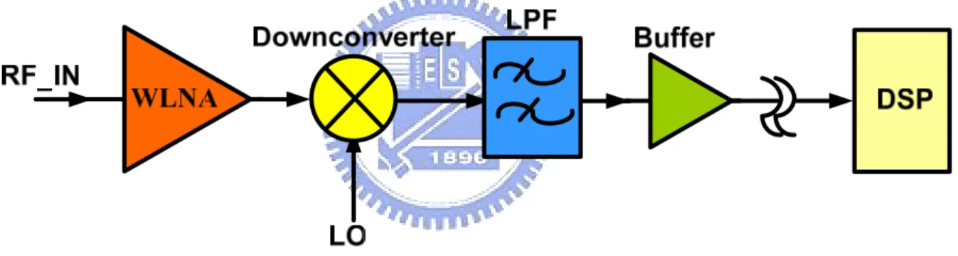
RF front-end receiver is a major component in wireless communication equipments which consists of a low-noise amplifier (LNA), down-converters, local oscillators (LO), filters and some baseband processing circuits. Conventionally, signal is received by the antenna, then goes through and amplified by LNA circuit. Down-converters mix the output of LNA and local oscillator (LO) signal generated by voltage-controlled oscillator to the desired intermediate frequency. Filters suppress the unwanted signals or interference to provide a moderate signal quality for the baseband processing circuits to reach a reasonable performance. However, in MB-OFDM UWB system, it is somehow different from the above mentioned narrow band receiver. As a result of the wide operating bandwidth, some circuit blocks are supposed to have a wideband character or multiple switched circuits used to work
3
at various frequency bands, and more than one single carrier frequency is required in the receiver chain for frequency down-conversion. Besides, what cannot be ignorable is that out-of-band disturbance must be taken into consideration and be analyzed carefully.
By carefully investigating the receiver architectures, zero-IF is best adopted for the design of UWB receiver, as shown in Figure 1.1. Though suffering from some well-known drawbacks such as DC offset, I/Q mismatches and LO pulling, zero-IF receiver inherently allows highest integration level which is highly desirable for low-cost applications: DC-offset issue can be eliminated in UWB applications due to its flexible utility of sub-channels in one UWB band [7],[10]. Some recently published works have been designed based on this architecture and are discussed in subsequent sections.
Figure 1.1 Architecture of zero-IF receiver
1.2.1 UWB Receivers
As UWB receivers are evolving continuously, several receivers have been published and analyzed. These receivers are mainly based on zero-IF architecture for its simplicity and advantage of low cost [9]-[12], [28]. The followings are representative reviews of the state-of-the-art UWB RF-front receivers.
A 0.13-μm UWB transceiver [9]
4
technology under 1.5-V supply and is shown in Figure 1.2. After the signal being amplified by
LNA at some desired band is down-converted to baseband frequency and processed by
subsequent baseband circuits. This receiver inevitably leads to a tradeoff among cost, power, and bandwidth. Each circuit component can merely handle one signal band of interests, and therefore it requires more circuit blocks and complicated switching mechanism to fulfill the applications of full band UWB system. Besides, it consumes too much extra power to reach little bandwidth increment and the use of passive elements would be a critical issue (narrow band LC tank is sensitive to process variation) and occupies a large chip area.
Figure 1.2 Block diagram of [9]
A 3.1 ~ 8.2 GHz RF front-end for MultiBand UWB wireless receivers [10]
The receiver is implemented in SiGe 0.25-μm technology and operates under 2.5-V supply voltage. Figure 1.3 shows the block diagram of the receiver: a wideband LNA is
5
capable of amplifying input signal at 3.1~8.2 GHz , a frequency synthesizer with only one
VCO osccilating at 16 GHz is employed to generate required carriers, LPFs are used as mixer
load, and VGAs(variable gain amplifier) are used to boost signal amplitude level before baseband processing. Though the receiver architecture greatly simplifies the design of UWB receivers, it suffers from some main drawbacks such as high power consumption under 2.5-V supply and inevitable poor integrity with baseband CMOS circuit, which makes this receiver uneasy to combine with future works.
Well, a CMOS receiver covering as much UWB bands with as fewer circuit components attracts more and more attention and is placed great emphasis on low-cost and low-power applications: this trend is ongoing all the time.
Figure 1.3 Block diagram of [10]
1.3 Motivation
Some published receivers for UWB applications have been reviewed and surveyed. Based on the drawbacks of previous works and considerations mentioned above, an attempt to
6
design a low power, full band receiver front-end for UWB applications has come to play. The design of the receiver would try to realized a 3.1~10.6 GHz direct-conversion receiver in TSMC 013-μm technology under 1.2-V supply voltage. The constructing circuit components of the receiver would consist of a WLNA, aimed at possessing wideband input matching, low noise, and sufficient gain at low power consumption simultaneously; a carrier generator, designed to provide full-band quadrature LO signals with moderate phase noise and sufficient output power; down-conversion mixers, used to down-converted input signal to baseband frequency; output buffers, used for measurement consideration.
The receiver is fulfilled according to IEEE 802.15 TG3a specification, which specifies an operating spectrum for Multiband-UWB (MB-UWB) from 3.1 to 10.6 GHz and divides it into 5 band groups and 14 bands with spacing of 528MHz. The basis access is based on QPSK modulation and minimum input power level is -78.5 dBm.
1.4 Thesis Organization
Chapter 2 describes the detailed specification of IEEE 802.15 TG3a, design considerations of the receiver, and the proposed 3.1~10.6 GHz direct-conversion receiver is introduced. In Chapter 3, the circuit components of the receiver are presented: wideband LNA, carrier generator, and down-conversion mixer. The design consideration of each component would be illustrated and theoretic analyses are made together with simulation results. Chapter 4 contains experimental results and discussion. Finally, conclusion and future work are presented in chapter 5.
7
Chapter 2
A 3.1~10.6 GHz CMOS Direct-conversion receiver
To get a thorough understanding of the UWB system, the physical layer proposal for IEEE 802.15.3a is introduced and analyzed. And also, the system design considerations, theoretical analysis, as well as architecture of the proposed receiver are discussed and presented in chapter 2.
2.1 Multi-Band OFDM Physical Layer Proposal for IEEE
802.15 Task Group 3a
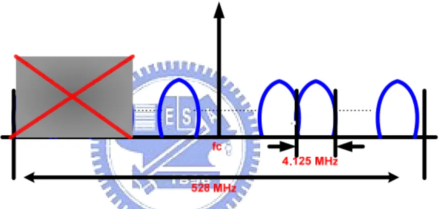
The IEEE 802.15 TG3a [6] specifies the unlicensed 3.1~10.6 GHz UWB band for short -range and high data-rate communications. The specified 7.5 GHz spectrum is divided into 5 band groups and 14 bands with spacing of 528 MHz as shown in Figure 2.1. The band center frequencies are given as:
b b
Band center frequency 2904 528 n (MHz) n= + × , =1...14 (2-1)
where nb represents band numbers. Band #1~Band #3 are used for Mode 1 application
(mandatory mode), while Band #1~Band #3 and Band #6~Band #9 are used for Mode 2 application (optional mode). The remaining channels are reserved for future use. The UWB system provides a wireless PAN with data payload communication capabilities of 55, 80, 110, 160, 200, 320, and 480 Mb/s. It incorporates orthogonal frequency division multiplexing (OFDM) modulation using quadrature phase shift keying (QPSK), a technique that uses multiple carriers to mitigate the effect of multipath path fading. Each 528 MHz band is divided into 128 sub-carriers resulting in a sub-carrier bandwidth of 4.125 MHz. Among the 128 sub-carriers, 100 tones carry payload data, 12 pilot tones facilitate coherent detection
8
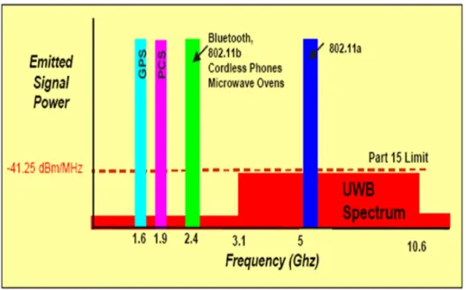
against frequency offset, and the other 6 null tones carry no information at all. The standard further defines a low transmitting power of -41.3 dBm per mega hertz for UWB systems, which allows the possible coexistence with other living standards like IEEE 802.11 a/b/g, IEEE 802.15.3, IEEE 802.15.4 and Microwave oven…and so on, as shown in Figure 2.2.
Figure 2.1 Frequency plan of MB-OFDM UWB systems
9
2.2 System Design Considerations
UWB system is quite dissimilar to conventional narrow band ones in some aspects: output power level, data rate, operating bandwidth, co-existence with other standards…and so on. Therefore, the system design considerations should be modified (relative to the conventional) to get the appropriate features of it. Preliminarily, single-ended circuits take the priority for its low power consumption and smaller chip area as compared to differential ones, though it is liable to suffer from higher noise and second-order distortion. The following step is that each band in the specified operating frequency range can be viewed as a single scheme which acts like a conventional narrow system except more sub-carriers within. An extension is made to get the complete characteristics over the entire frequency bands and analysis of the influence of crossed relations between frequency bands. In addition, some challenges when implementing a full-band UWB receiver are discussed below [6]-[11]:
(1). A wideband input impedance matching is required that spans from 3.1 to 10.6 GHz. The LNA at the receiver front-end should provide low noise figure and sufficient gain at low current consumption.
(2). When receiving one channel, signals in other channels enter the receiver and appear as blockers. As a result, in addition to in-band linearity constraints, the wideband receiver is vulnerable to out-of-band compression. While in-band compression can be mitigated with automatic gain control, the cascaded receiver chain should be sufficiently linear to prevent out-of-band compression. The problem is illustrated in Figure 2.3: if the in-band signal (Band #2) is weak, a strong interferer (Band #5) desensitizes the receiver chain and degrades the desired signal gain. The worst case happens once the blocker gets close to the signals of interests in the frequency plan. (3). A new linearity constraint different from narrow band systems arises due to the
10
band systems harmonic distortion due to second-order nonlinearity is usually ignored, since it lies out of band. However, in this wideband receiver, second-order distortion from Band #1 falls into Band # 6, which seriously jams signals after down-conversion to baseband. The analysis can be further described as below: For input signal of Vin(t) A Cos= 1 ω1t A Cos+ 2 ω2t , and an input-output
characteristic of the amplifier:
2 3
1 2 3
Vout= ∂ Vin+ ∂ Vin + ∂ Vin "
(2-2)
The second-order term in (2-2) results in output components located at the frequencies ofω1±ω2 ,2ω1 ,2ω2 as shown in Figure 2.4. Given that ω1 is 3.342
GHz and ω2 is 6.684 GHz, now, if signal at ω1 is down-converted to basedband, the
inter-modulated term of at (ω2-ω1) would also be transferred to baseband. However,
if signal at ω2 is the wanted one, then harmonics at 2ω1 is down-converted to
baseband and hence jams the wanted signal: ω1 ± ω2.
(4). Spurs on the LO signal, even ones that are far away, can down-convert in-band signals to the same frequency as the wanted band, as shown in Figure 2.5. This case is usually more apparent in LO signals generated by direct frequency synthesizer. The issue is somehow relaxed in this UWB receiver realization, for which LO signals are generated with carrier generator that avoids the happening of spurs located in contiguous bands.
(4). Wideband systems use complex modulation schemes, whose crowded constellations place greater demand on gain balance between I and Q channels, and on quadrature accuracy of LO phases.
11 #1 #2 #3 #4 #5 #6 #7 #8 #9 #10 #11 #12 #13 #14 3432 MHz 3960 MHz 4488 MHz 5016 MHz MHz5544 6072 MHz 6600 MHz 7128 MHz 7656 MHz 8184 MHz 8712 MHz MHz9240 9728 MHz 10296 MHz f
Out-of-band case
In-band case
Figure 2.3 Out-of-band compression of the signal in band #2 due to interferer in band #8
Figure 2.4 Cross-band modulation due to second order nonlinearity
12
(6). As mentioned in previous section, direct-conversion architecture is suitable for UWB systems for its high integration capability, low-cost, and simple architecture. And the troublesome DC offset issue which comes from devices mismatch or imperfections encountered in most direct-conversion receivers can be eliminated due to its flexible utility of sub-channels in one UWB band as in Figure 2.6. That is to say if the aforementioned 4.125 MHz sub-carrier bandwidth does not carry any information at DC, therefore the DC offset cancellation can be greatly simplified by inserting a DC-notch filter at analog baseband with little influence on data transformation.
Figure 2.6 Flexible utilization of sub-channels
Then, according to link budget of IEEE 802.15.tg 3a standard, shown in Table 2.1, we can determine the target of the receiver design which includes frequency range, input-referred 1-dB compression point, noise figure, and overall receiver gain.
The specified noise figure is 8.6 dB and is regarded as the worst-case situation. We can also derive the maximum input power, shown as the following:
in,max T T,ATN R,ATN
P P +G +G -min_path_loss_L1- min_path_loss_L2 =-34.5 dBm = cm 10 log 20 _L2 _ _ min ) 4 ( log 20 _L1 _ min_ 10 = = = d d loss path C f loss path π c
13 PT:maxium transmitting power
GT:transmitter antenna gain
GR:Receiver antenna gain
d:the distance between the communicating devices C:3x10⁸
m/s
(2-3)
However, as a conservative rule of thumb, the input referred 1-dB compression point should be around 4 dB higher than the maximum input signal power level that should be tolerated successfully. On the basis of the approximation, the target of worst-case input referred 1-dB compression point is set to -30 dBm. Therefore, the required performance of each circuit block can be estimated to get the 802.15.TG 3a specification for the thesis and is listed in Table 2.2.
For noise figure performance of each component in the direct-conversion receiver design, it can be evaluated by the given overall front-end noise figure and be expressed as:
2 m tot 1 p1 pm (NF -1) (NF -1) NF 1 (NF 1) +...+ A A ≈ + − + (2-4)
, where NFtot is given as 8.6 dB, NFm is the noise figure of each stage with respect to the
source impedance driving that stage and Apm represents the gain of each stage. This is called
Farris equation [2]. The input IP3 for third order non-linearity is obtained with the general
expression of cascaded stage and the relation with input 1 dB compression point shown below.
(2-5)
Simultaneously, the phase noise performance of direct-conversion receiver can be calculated. P1 Pm
2 2 2 2
IP3 IP3,1 IP3,2 IP3,m IP1 IP3 1 1 A A + + + A A A A A -9.6 dB A = = "
14
For the OFDM UWB systems, phase noise requirements of local oscillator are primarily determined by two factors: inter-carrier-interference (ICI) and power levels of in-band, out-of-band blockers. While the ICI requirement for MB-OFDM systems is relaxed due to its large sub-carrier bandwidth, strong out-of-band blockers dominates the LO phase noise consideration. For an out-of-band blocker fm away from the center of desired UWB band, the
corresponding phase noise is required to be lower than m
L(f )=PS −SNR_PB −10log(BW)
(2-6)
Where PS is the power level of received UWB signal specified in [5] as 6 dB higher than RX
sensitivity;PB is the power level of the blocker;SNR is the required signal-to-noise-ratio (4
dB for 110 Mb/s data rate) and BW is the UWB bandwidth. In order to have a fair comparisons, phase noise limits at different frequencies should be all normalized to values at 1MHz offset. Assuming the far-out LO phase noise follows characteristics of 1/f2; the normalized phase noise can be expressed as:
L(1 MHz) ( ) 20log( ) ( / ) 1 m m f L f dBc Hz MHz = + (2-7)
While the voltage gain for first stage of the receiver, LNA, is recommended as 15 dB in the standard, the design target of the direct-conversion receiver and its building block can be obtained through these analyses and is listed in Table 2.2. Although the analytic steps are the same as conventional narrow band systems, the UWB system has a much wider operational bandwidth. Therefore, the specified performance should maintain stable during the wide operational frequency range.
15
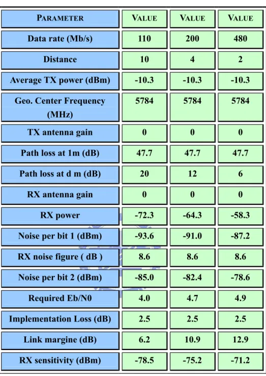
Table 2.1 Link Budget for MB-OFDM UWB System
PARAMETER VALUE VALUE VALUE
Data rate (Mb/s) 110 200 480
Distance 10 4 2
Average TX power (dBm) -10.3 -10.3 -10.3 Geo. Center Frequency
(MHz) 5784 5784 5784 TX antenna gain 0 0 0 Path loss at 1m (dB) 47.7 47.7 47.7 Path loss at d m (dB) 20 12 6 RX antenna gain 0 0 0 RX power -72.3 -64.3 -58.3 Noise per bit 1 (dBm) -93.6 -91.0 -87.2 RX noise figure ( dB ) 8.6 8.6 8.6 Noise per bit 2 (dBm) -85.0 -82.4 -78.6
Required Eb/N0 4.0 4.7 4.9
Implementation Loss (dB) 2.5 2.5 2.5 Link margine (dB) 6.2 10.9 12.9 RX sensitivity (dBm) -78.5 -75.2 -71.2
16
Table 2.2 The IEEE 802.15.TG 3a specification for this thesis
Frequency Range 3.1 ~10.6 GHz Max input power -34.5 dBm
Noise figure 8.6 dB
P1dB >-30 dBm
Band numbers 14
Band bandwidth 528 MHz
Table 2.3 The specification of the proposed direct-conversion receiver and its circuit component
VDD 1.2 V Gain >15 dB NF <8.6 dB P1dB >-30 dBm Front-End Receiver Power <60 mW Gain 15 dB NF <4 dB LNA P1dB >-20 dBm Gain 0 dB NF <15 dB Donw-conversion Mixer P1dB >-13 dBm Tuning Range 2.9~10.4 GHz Carrier Generator Phase Noise <-90 dBc
17
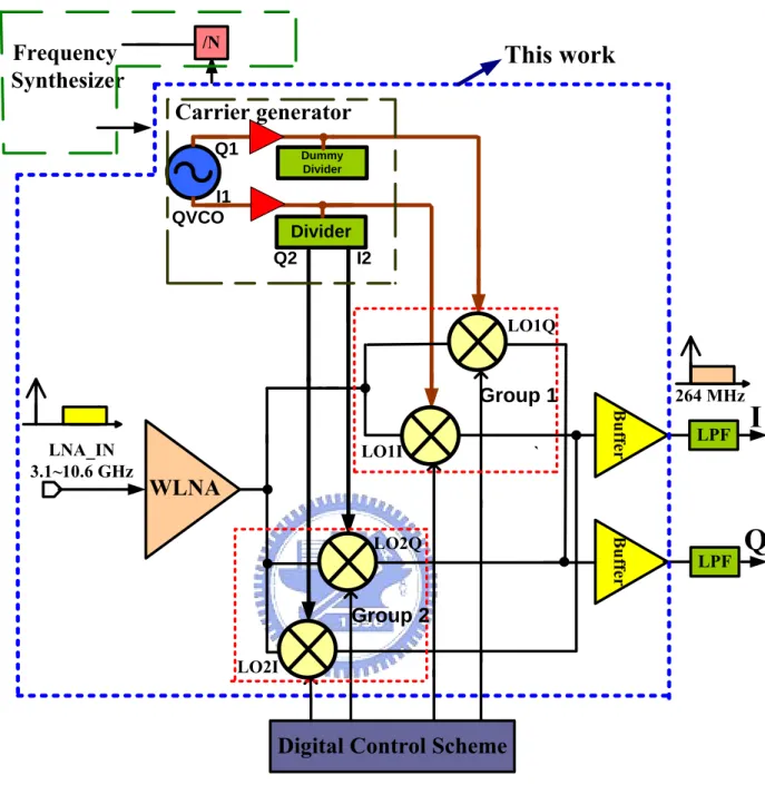
2.3 Receiver Architecture and Operational Principle
The block diagram of the proposed receiver is shown in Figure 2.7, which consists of a wideband LNA (WLNA), I/Q quadrature down-conversion mixers, output I/Q buffers and a carrier generator. The RF input signal is amplified by the WLNA first and two I/Q down-conversion mixer groups follow the WLNA. The down-conversion mixers are classified into two groups: group one handles the lower band (3.1~5.5 GHz) signals and group two deals with the higher band (5.5~10.6 GHz) signals. By mixing with proper LO signals provided by the carrier generator, the frequency is translated to DC. Extra digital control scheme is used to determine which mixer group is on, thus the desired output signal can be generated at the output buffers. This arrangement of down-conversion mixers would help in solving the spur and harmonics issues which are much more critical in UWB systems than in conventional narrowband systems [7]. This could be explained as the following: While in this proposed receiver, the lower frequency (3.1~5.5 GHz) and higher frequency (5.5~10.6 GHz) signals are separated, thus the LO signals at 3.1~5.5 GHz and its harmonics will not fall in the higher band group. It avoids overwhelming the signal at baseband after down-conversion is executed and ease the difficulty of designing a wideband mixer. The carrier generator, one of the building blocks in a frequency synthesizer, is designed in this chip to provide required quadrature LO signals. Based upon the architecture shown in Figure 2.7, the CMOS implementation of WLNA, quadrature down-conversion mixer, and carrier generator is described in Chapter 3.
18
I
Q
` LO1I LO1Q LO2I LO2Q LNA_IN 3.1~10.6 GHzFrequency
Synthesizer
/N LPF LPF 264 MHzDigital Control Scheme
Group 1 Group 2
![Figure 1.2 Block diagram of [9]](https://thumb-ap.123doks.com/thumbv2/9libinfo/8462693.183249/17.892.133.811.464.1014/figure-block-diagram-of.webp)
![Figure 1.3 Block diagram of [10]](https://thumb-ap.123doks.com/thumbv2/9libinfo/8462693.183249/18.892.219.742.551.871/figure-block-diagram-of.webp)