國
立
交
通
大
學
電子工程學系 電子研究所
碩 士 論 文
考量跨電源供應域靜電放電與快速帶電器件模型分析之
平面規劃演算法
An ESD aware Floorplan Algorithm with Efficient CDM
Estimation for Multiple Power Domain Designs
研 究 生:林新鈞
指導教授:陳宏明 博士
考量跨電源供應域靜電放電與快速帶電器件模型分析之
平面規劃演算法
An ESD aware Floorplan Algorithm with Efficient CDM
Estimation for Multiple Power Domain Designs
研 究 生:林新鈞 Student:Hsin-Chun Lin
指導教授:陳宏明 博士 Advisor:Dr. Hung-Ming Chen
國 立 交 通 大 學
電子工程學系 電子研究所
碩 士 論 文
A Thesis
Submitted to Department of Electronics Engineering and Institute of Electronics
College of Electrical and Computer Engineering National Chiao Tung University
in partial Fulfillment of the Requirements for the Degree of
Master of Science in
Electronics Engineering
September 2013
Hsinchu, Taiwan, Republic of China
i
考
考
考量
量
量跨
跨
跨
電
電
電源
源
源供
供
供應
應域
應
域
域靜
靜
靜電
電
電放
放
放
電
電
電與
與
與快
快
快速
速
速帶
帶
帶
電
電
電器
器
器
件
件模
件
模
模型
型
型分
分
分析
析
析之
之
之平
平
平
面
面
面規
規
規劃
劃
劃演
演
演算
算
算法
法
法
研究生:林新鈞 指導教授:陳宏明教授 國立交通大學 電子工程學系 電子研究所摘
摘
摘 要
要
要
當電晶體逐步的縮小,元件的可靠性上的問題變得更加重要。更小的電晶體,因 此有更薄的電晶體管閘極氧化層,這意味這電晶體更容易在靜電放電(ESD)的事件受 傷害。在三個ESD模型之中,由於帶電器件模型(CDM)其更快和更大的放電電流, 導致災難性損壞的可能性較大。其他兩個ESD模型,人體模型(HBM)和機器模型 (MM),所導致的損壞可以有效地在元件階段被保護。但是,因為CDM事件的不可 預測性,保護對CDM的事件是更複雜的,雖然以前的研究在元件階段上實施ESD保護 方法,我們提出了一種高效和有效的方法,在設計階段能夠防止CDM事件。當佈局規 劃是確定的,我們提出了一個根據聚集分析的電源箝位器擺放演算法去擺放電源箝位 器在優越的位置,能有效減少電源箝位器的數量,同時達到比常規方法更好的保護。ii
An ESD Aware Floorplan Algorithm with Efficient
CDM Estimation for Multiple Power Domain Designs
Student: Hsin-Chun Lin Advisor: Dr. Hung-Ming Chen
Department of Electronics Engineering Institute of Electronics
National Chiao Tung University
ABSTRACT
The issue on reliability of the device becomes more critical as transistor progressively scales down. Smaller transistor and hence thinner gate oxide implies transistors are more vulnerable against an Electrostatic Discharge (ESD) event. Among the three models in ESD, Charged Device Model (CDM) has the greater potential to deal catastrophic dam-age to the device due to its faster and larger discharging current. Damdam-age induced from the other two ESD models, human body model (HBM) and machine model (MM) can be effectively protected at device stage. However, protection against a CDM event is much more sophisticated due to its unpredictability. While most previous works on ESD protec-tion methodology are implemented at device stage, we propose an efficient and effective methodology to protect against a CDM event at design stage. When floorplan of a design is determined, we propose a power clamp placement algorithm derived from clustering analysis to place power clamp at strategic location which can effectively minimize number of power clamps while achieving better protection compared to conventional method.
Contents iii 致 謝 感謝我的指導教授 陳宏明老師,讓我對EDA的領域有更深層的領悟並在研究的道 路上給予我指引,很慶幸能夠在老師的教導下做研究,也讓我有機會加入VDA的大家 庭。 感謝VDA的學長姐們,在我遇到困難時,隨時伸出援手,在我遇到問題時,不厭其 煩的教導我,Sean、BenBean、Jerry、篤雄、俊凱、敬雨,真的很感謝你們這兩年的 提攜與教導;仁國、鈞鴻、建志、冠廷,感謝你們在生活上為我帶來各種歡樂,讓我 的碩士生涯中添了一筆色彩。 感謝VDA的同學和學弟妹們,川嘉、以恩、天龍、孟伶,謝謝你們在課業上以及生 活上給予我各種幫助,以及研究遇到困難時給我方向;韋辰、家麒、柔君,謝謝你們 在各種細節上的打點,讓我沒有後顧之憂。 感謝我的大學同學們,各種的小聚會讓我的生活充滿快樂。 感謝我的室友們,秉辰、睿綱、昱全、承翰、哲仲、菘昀、唯家、芝佑、佳歆,讓 我度過一段愉快的碩士生涯。 感謝我的父母,讓我能夠全心全力的求學。謝謝你們。 感謝錐錐,總是用快樂迎接我。謝謝妳。 感謝采芸,陪我度過低潮、陪我分享快樂。謝謝妳。 太多感謝無法用文字表達,但是我的生活卻因你們而精采,謝謝你們。
Contents
Abstract (Chinese) i Abstract ii List of Figures v List of Tables vi 1 Introduction 1 1.1 Previous works . . . 21.2 Contributions of this work . . . 3
2 Preliminary 6
3 Effective CDM Simulation using Static Power Analysis 9
3.1 Power Network Model for Charged Device . . . 9
3.2 Solving the Power Network Model . . . 12
3.3 Obtaining CDM level of the device . . . 13
4 Clamp Placement 15
4.1 Peripheral Power Clamp Placement . . . 15
4.2 Power Clamp Placement Based on Pin Location . . . 17
5 Experimental Results 19
5.1 Analysis on Power Clamp Placement . . . 20
List of Figures
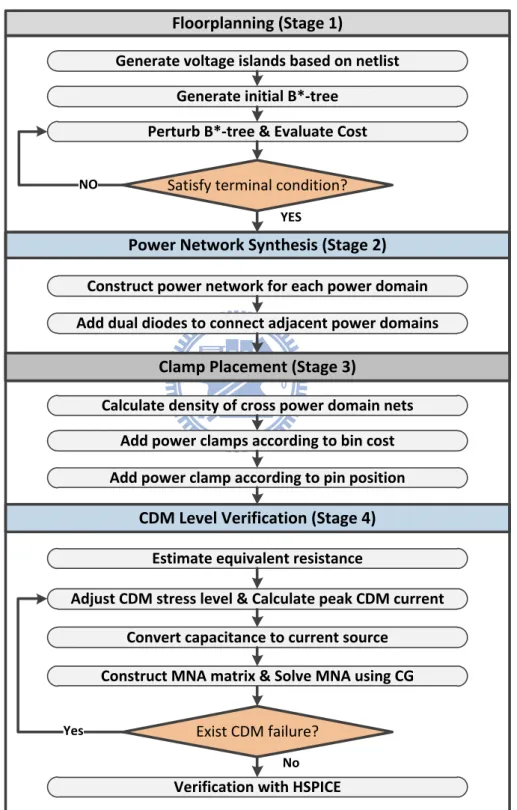
1.1 Flow chart of the proposed framework. . . 4
2.1 Schematic of a receiver and receiver between two power domains. . . 7
4.1 Voltage distribution of VDD and VSS power domain at the instant when stress pin is grounded. Power clamp is positioned right next to the stress pin. The two white rectangles represent two individual power domains. (a) Voltage distribution of VDD power domain. (b) Voltage distribution of VSS power domain. . . 16
List of Tables
3.1 Comparison on error of voltage for CG and HSPICE . . . 13
5.1 Power Network Synthesis setting . . . 19
5.2 Detail of the input benchmarks. (P.D. stands for number of power domains excluding chip power domain. Net stands for number of netlist. P.D. 2-Pin net stands for number of cross power domain 2-pin nets. Internal I/O Pin stands for number of internal I/O pins. I. Module stands for number of internal modules within the voltage island. E. Module stands for number of external modules connected to the voltage island.) . . . 21
5.3 Comparison on CDM level and number of power clamps using Uniform, Pin+Peripheral and Cluster+Peripheral. (CDM stands for CDM level. C.# stands for number of power clamps.) . . . 22
Chapter 1
Introduction
Electrostatic Discharge (ESD) is a major issue in chip’s reliability. As feature size de-creases, the increase in metal density makes device more vulnerable to surge current [1]. Sudden surges current is capable of dealing great damage to the core circuit and ulti-mately impair chip functionality. Hence, employing a full-chip ESD protection strategy is an essential criterion in modern design.
There are standard ESD test released by ESDA [2] and JEDEC [3] which includes human-body model(HBM), machine model(MM) and charged device model(CDM). Both HBM and MM assumes the initial charge is stored in an external storage and current is dis-charged from the external storage through the device. Thus, HBM and MM requires two arbitrary pins connect from external storage to the device to complete the discharge path. The difference between HBM and MM is that HBM assumes initial charge is stored in human while MM assumes initial charge is stored in machine. On the contrary, CDM as-sumes initial charge is stored in the device and current is discharged from the device when an arbitrary is grounded. The grounded pin during a CDM event is generally referred as stress pin. A CDM event is capable of delivering severe damage to the device due to its higher peak current and shorter rise time compared to HBM and MM event [4].
ESD Protection against HBM and MM can be effectively achieved by placing ESD pro-tection circuit next to the I/O pin [5]. However, ESD protection against a CDM event is much more sophisticated since its initial charge is stored within the device and discharge
Chapter 1. Introduction 2 path begins from inner core to the stress pin. A CDM event can be triggered from any part of the device and discharged to any external I/O pin. It is impossible to predict which region of the device will trigger a CDM event and discharge to which external I/O pin. Thus, to protect against a CDM event, modern design flow places power clamp circuits to offers low resistance paths to channel the surge current in attempt to protect vulnerable transistors [6]. The placement of clamp circuits generally relies on designer’s experience. A CDM event can deliver potential damage to internal circuit of the design or internal I/O pins (transceiver/receiver) between two power domains. According to reported statistics, most CDM events occur at the gate oxide of input receiver between two power domains [7]. A transistor can withstand a certain level of threshold voltage between the gate and source end before the gate oxide ruptures. This threshold voltage is generally referred as break down voltage. A device can withstand a certain level of cross voltage before any of its transistor breaks down. The level of cross voltage a device can withstand is generally referred as CDM level of a design. The higher CDM level of a design, the more robust the design is against a CDM event.
1.1
Previous works
There are several previous works on CDM simulation and modeling [6–10]. The work done in [6] analyze the effect of clamp placement, package substrate and decoupling capacitance contribute to a CDM event. In [8], a chip-level simulation methodology for CDM failure analysis is proposed. The key components of design are replaced with individual macro model and CDM model of the entire design is constructed in a hierarchical fashion. In [10], a simulation methodology is proposed based on static power analysis. However, the work done in [10] does not consider CDM failure for internal I/O or transceiver and receiver between two power domains. In addition, effect of capacitors is neglected.
Chapter 1. Introduction 3
1.2
Contributions of this work
Although it is very difficult to accurately simulate a CDM event due to its inherent random nature, regions of the device that is vulnerable to a CDM event can be easily identified. While previous works have done extensive analysis to simulate a CDM event, the time complexity to achieve great accuracy forbids it to integrate within an iterative optimization framework. In this regard, the objective of this work is to effectively and efficiently increase device’s ability to withstand a CDM event at early design stage. CDM level of a device is dominated by a primary factors, location of power clamps of the device. Our framework includes a CDM simulation model based on static power analysis and power clamp placement algorithm. These two key components are essential for a complete CDM protection strategy.
When floorplan is determined, a pseudo power network is synthesized for each power domain. Power clamps are then placed at strategic locations to maximize CDM level of the device. The CDM simulation model that serves to check CDM failures is tightly integrated to the framework. Our proposed methodology is a stand-alone binary and can be employed at early design stage. To the best of our knowledge, this is the first work on power clamp placement for CDM optimization at design stage. In brief, our contributions can be summarized as follows.
• We propose a CDM simulation algorithm which can identify vulnerable region at design stage. Our simulation analysis is compared with HSPICE and has an average deviation within 0.11%.
• Given a design with determined floorplan, we propose an effective and efficient clamp placement algorithm to increase device’s ability to defend a CDM event.
Fig.1.1is a flow chart of the proposed framework. Our proposed framework consists of four stages. The first stage is floorplanning which is built based on B∗-tree data structure. The second stage synthesize a pseudo mesh based power network on the given floorplan with pitch width, wire spacing, sheet resistance and via size based on UMC 65nm technology
Chapter 1. Introduction 4
Generate voltage islands based on netlist
Floorplanning (Stage 1)
Power Network Synthesis (Stage 2)
CDM Level Verification (Stage 4)
YES
Generate initial B*-tree Perturb B*-tree & Evaluate Cost
Satisfy terminal condition?
Construct power network for each power domain Add dual diodes to connect adjacent power domains
Estimate equivalent resistance
Adjust CDM stress level & Calculate peak CDM current
Exist CDM failure?
No Yes
Construct MNA matrix & Solve MNA using CG Convert capacitance to current source
NO
Clamp Placement (Stage 3)
Add power clamps according to bin cost Add power clamp according to pin position
Verification with HSPICE
Calculate density of cross power domain nets
Figure 1.1: Flow chart of the proposed framework.
file. The third stage place power clamps at strategic location to increase CDM level of the device. The fourth stage solves the power network using iterative method and verifies the result with HSPICE.
Chapter 1. Introduction 5 concept of CDM. Then, Chapter 3 presents an effective CDM simulation algorithm using static power analysis. Chapter 4 introduces a power clamp placement algorithm based on clustering analysis. Chapter 5 presents experimental results. Finally, chapter 6 concludes this work.
Chapter 2
Preliminary
Given a charged device, the charge stored in the device is within the metal layers of power network. When an arbitrary external I/O pin is grounded, the charge stored in the device is discharged through the stress pin. A typical CDM event has a very short rise time. The current value at stress pin can reach its peak value within 0.2ns. As current is discharged through stress pin, if the cross voltage between transistor’s gate and source end, Vgs, exceeds the break down voltage, gate oxide of the transistor is at high risk of
being ruptured.
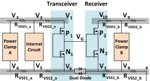
Fig. 2.1 is a schematic illustration of a transceiver and receiver between two power do-mains. In Fig. 2.1, transistor P1 and N1 correspond to the PMOS and NMOS of the
transceiver. Transistor P2 and N2 correspond to the PMOS and NMOS of the receiver.
The voltage drop of N2 can be expressed as Eq. (2.1) and the voltage drop of internal
circuit can be expressed as Eq. (2.2).
Vgs,N2 = VG− V7 (2.1)
Chapter 2. Preliminary 7 Power Clamp B Power Clamp A VSS2_b
R
VSS1_bR
VDD2_bR
7V
V
8 P 6V
1V
2V
3V
Dual DiodeReceiver
Transceiver
VDD1_aR
VSS1_aR
R
VSS2_a 4V
1P
1N
VDD2_aR
R
VDD1_b 5V
GV
P
2 2N
Internal Circuit 9V
10V
Figure 2.1: Schematic of a receiver and receiver between two power domains.
Since the device is disconnected from the power source before an ESD event, the voltage value at the gate pin of PMOS is logic 0 which means PMOS is activated and NMOS is de-activated when device is disconnected from the power source. In Fig. 2.1, VG is
approximately equal to V1 and Eq. (2.1) can be rewritten as Eq. (2.3) in which Vgs,N0 2 is
the approximated value for Vgs,N2.
Vgs,N2 ≈ V
0
gs,N2 = V1− V7 (2.3)
V1− V7 = (V1− V 2) + (V2− V 3) + (V3− V4)
+ (V4− V 5) + (V5− V 6) + (V6− V 7) (2.4)
In Eq. (2.3), the threshold voltage for transistor N2 is approximately the cross voltage
between VDD stripe and GND stripe. In other words, the cross voltage between V1 and
V7 must not exceed the break down voltage of N2 to ensure the functionality of N2.
The resistive path between V1 and V7 or the right hand side of Eq. (2.3) can be expressed
Chapter 2. Preliminary 8 RV DD2 a. V3− V 4 represents the voltage drop across the power clamp at the transceiver
power domain. V4− V6 represents the voltage drop across resistor RV SS1 a and RV SS2 a.
V4− V5 represents the voltage drop across the dual diode connecting two power domains.
Eq. (2.4) implies that Vgs,N2 is affected by two main factors. The first factor is the location
of power clamp. The cross voltage value of V1 − V3 and V4− V6 is proportional to the
distance between the power clamp and the transceiver. Thus, the farther away the power clamp is placed away from the transceiver, the larger value is for V1− V3 and V4− V6. The
second factor that affects Vgs,N2 is distance between two power domains. The distance
between two power domains is proportional to the cross voltage value of V6− V7.
Regarding Eq. (2.4) and Eq. (2.2), it can be easily observed that receiver or N2 suffers
much larger voltage drop compared to internal circuit. Note that the example illustrated in Fig. 2.1 does not include all scenarios. Depends on the structure of internal circuit, a CDM event can still occur at internal circuit. However, receiver between two cross power domains is generally more vulnerable to a CDM event based on reported statistics. Based on Eq. (2.3) and Eq. (2.4), the CDM level of a given device is largely affected by placement of power clamps and the distance between two power domains with signal transmitting between two power domains. In this regard, if floorplan of a given design is determined, CDM level can still be improved by adjusting placement of power clamps. If floorplan can be adjusted, CDM level can be further improved by adjusting location of power domains.
Chapter 3
Effective CDM Simulation using
Static Power Analysis
To simulate a CDM event, the device needs to be disconnected from the ground and then charge the device through the power network to a certain voltage value. The voltage value a device can withstand without any transistor breaks down is commonly referred as VCDM of the device. The process of charging the device is generally referred as pre-charge
stage. When an arbitrary pin of a charged device is grounded, the stored charge within the device is discharged to the ground through the stress pin.
Here, we briefly summarize our simulation methodology. Given with a multiple power domain design, a mesh based pseudo power network is synthesized for each individual power domain. The synthesized power network is converted to a RC network. Then the device is charged to a certain voltage level. After the device is charged, a power analysis is initiated to examine any CDM Failures.
3.1
Power Network Model for Charged Device
The long execution time of transient power analysis makes it impractical to integrate in the iterative framework. Since the primary objective is to accurately measure the maximum
Chapter 3. Effective CDM Simulation using Static Power Analysis 10 value of Vgs,i and due to the short duration of a CDM event, static power analysis is more
than sufficient compared to transient power analysis.
To conduct static power analysis on a RC network, the capacitors in the RC network needs to be replaced with current sources. The value of current source is defined in Eq. (3.1) in which Qi denotes the charge stored within the capacitor and IP eak denotes the peak
current at the stress pin when device is discharged through the stress pin. The total value of charge stored in each capacitor is defined in Eq. (3.2). To obtain the current source value Ii, Qi and IP eak must be determined.
Ii = Qi QT ot. IP eak (3.1) QT ot. = n X i=1 Qi (3.2)
After pre-charge is complete, the voltage value for all capacitors is charged to VCDM. The
amount of charge stored in each capacitor can be represented in Eq. (3.3) in which Ci
denotes the capacitance for the capacitor.
Qi = CiVCDM. (3.3)
During a CDM event, charge stored in each capacitor flows through the power network and then discharges through the stress pin into ground. Based on Eq. (3.3), the total amount of charge flowing through the stress pin can be calculated using Eq. (3.4). In Eq. (3.4), N is total number of capacitors, t denotes a certain time frame and Req,i denotes the
Chapter 3. Effective CDM Simulation using Static Power Analysis 11 QDis. = N X i=1 CiVCDM(1 − exp−t/Req,iCi) (3.4)
Based on Eq. (3.4), the current value flowing through the stress pin can be obtained using Eq. (3.5) in which 4t denotes the sampling period. The peak current at the stress pin is defined in Eq. (3.6) IDis.= δq δt = QDis.(t + 4t) − QDis.(t) 4t (3.5) IP eak = max( QDis.(t + 4t) − QDis.(t) 4t ) (3.6)
To obtain the exact value of Req for each capacitor is time consuming. Hence, we use an
effective method to approximate the value of Req. First, the RC network is partitioned
into n partitions. Second, a dummy current source is placed at the center of each partition and connected to the RC network. Third, voltage drop between each center of partition and stress pin is measured. Finally, the equivalent resistance for each center of partition is calculated using Eq. (3.7).
Rceq,j =
Vj − VP in
IDummy
(3.7)
In Eq. (3.7), Rceq,j is the equivalent resistance from center of partition j to the stress pin,
Vj is voltage value at the center of partition j and IDummy is the value of the dummy
current source. After the equivalent resistance of all center of partitions is calculated, the equivalent resistance of each capacitor Req,i is replaced by the equivalent resistance from
Chapter 3. Effective CDM Simulation using Static Power Analysis 12 By using the approximated equivalent resistance R0eq,ifor each capacitor, Eq. (3.4), Eq. (3.5) and Eq. (3.6) is rewritten as Eq. (3.8), Eq. (3.9) and Eq. (3.10) respectively. In Eq. (3.9), α is an adjustment coefficient based on the distance between partition center and capacitor.
Q0Dis. = n X i=1 CiVCDM(1 − exp−t/αR 0 eq,iCi) (3.8) IDis.0 = Q 0 Dis.(t + 4t) − Q 0 Dis.(t) 4t ≈ IDis. (3.9) IP eak0 = max(Q 0 Dis.(t + 4t) − Q 0 Dis.(t) 4t ) (3.10)
Finally, we can approximate the value of current source corresponding to each capacitor using Eq. (3.11). Ii0 = Qi QT ot. IP eak0 = CiVCDM CT ot.VCDM IP eak0 = Ci CT ot. IP eak0 (3.11)
3.2
Solving the Power Network Model
The power analysis performed on the obtained resistive network can be efficiently solved using Modified Nodal Analysis(MNA). The resistive network can be represented in Eq. (3.12). In Eq. (3.12), matrix G is the conductance matrix which represents each resistor in the power network, matrix I is the value of current source and matrix V is the unknown matrix which represents the voltage value at each point in the power network. Eq. (3.12) can be solved efficiently using methods proposed in [11–13]. In this work, we convert the
Chapter 3. Effective CDM Simulation using Static Power Analysis 13
Table 3.1: Comparison on error of voltage for CG and HSPICE
# Max Error Avg. Error Run Time of Spice Run Time of CG
(%) (%) (Sec.) (Sec.) n10 0.005497 0.001065 7.01 0.33 n30 0.028947 0.005067 6.6 0.37 n50 0.043068 0.012632 6.06 0.32 n100 1.471763 0.369787 5.38 0.21 n200 1.769588 0.17528 5.72 0.22 n300 0.027367 0.005279 8.58 0.38 Avg. 0.67 0.11 7.87 0.37
power network to TAU 2012 Static Power Analysis Contest benchmark format [14] and solve the problem using Jacobi-preconditioned conjugate gradient method. The result of our power analysis is compared with HSPICE. Table3.1 shows that the deviation of our power analysis compared with HSPICE is within 0.11%.
GV = I (3.12)
3.3
Obtaining CDM level of the device
Using the model described in Chpater 3.1 and solves the model using iterative method described in Chpater 3.2, the CDM level of a device can be obtained using binary search. Algorithm 1 describes the procedure to search for the CDM level of a given device. In Algorithm 1, given with the power network of the device, an upper bound value and a lower bound value, the algorithm begins to search for maximum CDM level the device can withstand such that no failure will occur.
Chapter 3. Effective CDM Simulation using Static Power Analysis 14
Algorithm 1 Obtain CDM level of the device Input: Power network of the device, D
Input: Upper bound and lower bound, Hi, Lo Output: CDM Level of the device, CL
1: do
2: T estV = (Hi + Lo)/2
3: F ailure = CDM-SIMULATION(D, T estV )
4: if F ailure then 5: Hi ← T estV 6: else 7: Lo ← T estV 8: end if 9: while (Hi − Lo <= 1) 10: CL ← Hi
Chapter 4
Clamp Placement
Placing power clamps can increase CDM level of a device. The challenge is to place mini-mal number of power clamps with most gain in CDM level. There are several power clamp placement methodologies adopted in industry. One approach is to place power clamp uni-formly across the device. Such approach provides a low resistance path for the surge current uniformly across the device, however, it requires large number of power clamps which is very inefficient. Another intuitive approach is to place one power clamp next to each internal I/O pins. However, such approach still neglects internal I/O pin density of the device. In this chapter, we first analyze the effect of power clamp placement to CDM level. Based on the analysis, a clamp placement algorithm is proposed to efficiently increase device’s CDM level using minimal number of power clamps.
4.1
Peripheral Power Clamp Placement
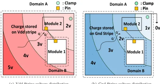
During a CDM event, the current discharge path begins from VDD(VSS) power domain through the power clamp to the VSS(VDD) power domain and discharge through the stress pin. Long discharge path creates larger voltage drop across the device due to longer resistive path. Larger voltage drop across the device implies that two power domains have higher probability to suffer larger voltage drop.
Chapter 4. Clamp Placement 16 Module 1 Module 2 Domain B Charge stored on Vdd stripe e Charge stored on Vdd stripe
Charge stored on Vdd stripe and Gnd Stripe
Domain Chip : Clamp
: Pin Module 1 Module 1 Module 1 Module 2 Domain B Charge stored on Vdd stripe e Charge stored on Vdd stripe
Charge stored on Vdd stripe and Gnd Stripe Module 1 Q Module 1 Module 2 Domain B Domain Chip e Charge stored on Vdd stripe Charge stored on Vdd stripe : Clamp : Pin
Charge stored on Vdd stripe and Gnd Stripe Q Q Module 1 Module 2 Domain B Domain Chip e : Clamp : Pin Charge stored on Vdd stripe and Gnd Stripe
Q Q Q Q Q Module 1 Module 2 Domain B Domain Chip : Clamp
: Pin Charge stored on Vdd stripe Charge stored on Vdd stripe Q Q 4v 0v 1v 2v 3v Module 1 Module 2 Domain B e : Clamp : Pin Domain A : Clamp : Pin Module 1 Module 2 Domain B Domain A : Clamp : Pin Charge stored on Vdd stripe Charge stored on Vdd stripe Q Q 4v 5v 6v Module 1 Module 2 Domain B Domain A : Clamp : Pin Charge stored on Vdd stripeQ Q 2v 5v 4v 3v Charge stored on Gnd Stripe Q Q
(a) Vdd Stripe voltage distribution
Module 1 Module 2 Domain B Charge stored on Vdd stripe e Charge stored on Vdd stripe
Charge stored on Vdd stripe and Gnd Stripe
Domain Chip : Clamp
: Pin Module 1 Module 1 Module 1 Module 2 Domain B Charge stored on Vdd stripe e Charge stored on Vdd stripe
Charge stored on Vdd stripe and Gnd Stripe Module 1 Q Module 1 Module 2 Domain B Domain Chip e Charge stored on Vdd stripe Charge stored on Vdd stripe : Clamp : Pin
Charge stored on Vdd stripe and Gnd Stripe Q Q Module 1 Module 2 Domain B Domain Chip e : Clamp : Pin Charge stored on Vdd stripe and Gnd Stripe
Q Q QQ Q Module 1 Module 2 Domain B Domain Chip : Clamp
: Pin Charge stored on Vdd stripe Charge stored on Vdd stripe Q Q 4v 0v 1v 2v 3v Module 1 Module 2 Domain B e : Clamp : Pin Domain A : Clamp : Pin Module 1 Module 2 Domain B Domain A : Clamp : Pin Charge stored on Vdd stripe Charge stored on Vdd stripe Q Q 4v 5v 6v Module 1 Module 2 Domain B Domain A : Clamp : Pin Charge stored on Vdd stripeQ Q 2v 5v 4v 3v Charge stored on Gnd Stripe Q Q
(b) Gnd Stripe voltage distribution
Figure 4.1: Voltage distribution of VDD and VSS power domain at the instant when stress pin is grounded. Power clamp is positioned right next to the stress pin. The two white rectangles represent two individual power domains. (a) Voltage distribution of
VDD power domain. (b) Voltage distribution of VSS power domain.
Thus, a general solution to reduce the current discharge path is to identify the location of the stress pin and place a power clamp right next to the stress pin. Placing power clamp next to the stress pin instantly discharge the current from VDD and VSS power domain which simultaneously reduces the discharge path. In addition, this placement method has a side benefit which is having similar voltage distribution for VDD and VSS power domain. Similar voltage distribution between VDD and VSS power domain implies that distance between two power domains linearly correlates to the voltage drop between two power domains. This is a desirable factor to the designers because reduction of cross voltage between two power domains can be simply achieved by moving two power domains closer. Fig. 4.1 illustrates the voltage distribution of VDD and VSS power domain when a power clamp is placed right next to the stress pin. However, since there is no known method to predict which of the external I/O pins will be grounded, a safe approach is to place a power clamp around the peripheral boundary of the device with uniform spacing. Placing power clamps around the peripheral boundary is a general approach to improve CDM level of the device regardless of the module’s location.
Conventional clamp placement methodology places a power clamp next to each internal I/O pins. The concept behind methodology is to minimize the current discharge path between transceiver and receiver. However, since each power clamp reduces voltage drop of
Chapter 4. Clamp Placement 17 neighboring range within a certain radius, placing a power clamp next to each internal I/O pin is redundant for regions with high pin density. By adopting k-means clustering [15], we propose a clamp placement algorithm that minimizes the distance from internal I/O pin to its nearest power clamp. The problem is constrained such that power clamp can only be placed at the location of internal I/O pin. We define the constrained power clamp placement problem as follows.
The constrained power clamp placement problem. Given the location of internal I/O pins P = {p1, p2, ..., pk}, place minimal number of power clamps such the distance from each
internal I/O pin to its nearest power clamp is minimized. Power clamp can only be placed at the location of internal I/O pins.
Regarding to Fig.4.1, a sharp voltage drop at VSS domain can be observed at peripheral boundary. The reason behind the sharp voltage drop is because stored current converge at the stress pin which is located at the peripheral boundary and thus creating large cross voltage between VDD and VSS domain. Thus, during a CDM event, modules that are placed near the peripheral boundary are prone to suffer larger voltage drop compared to modules located in center of device. To motivate more power clamps placed at peripheral boundary, a set of pseudo I/O pins are added around the peripheral boundary.
4.2
Power Clamp Placement Based on Pin Location
Algorithm2 describes the procedure to place power clamps by adopting clustering tech-nique. The algorithm begins by selecting pin closest to the bottom left corner as the initial location to place the first power clamp. In Line 10-23, after a new power clamp is placed, each pin updates the distance to its nearest power clamp. In line 24, pin with the maximum distance to its nearest power clamp is selected as the next location to place power clamp. The iterative process terminates until the maximum distance from each internal I/O pin to the nearest power clamp is less than a pre-define range. In this work, α is set to 80.
Chapter 4. Clamp Placement 18
Algorithm 2 Power Clamp Placement Based on Pin Location Input: Location of internal I/O pins P = {p1, p2, ..., pk}
Output: Location of power clamps C = {c1, c2, ..., cm} 1: MINDIST(pi) = ∞ ∀ i = 1 → k
2: j = 1
3: C ← ∅
4: pbl ← pin closest to the bottom left corner 5: Add new power clamp cj at location of pbl 6: Add location of cj to C
7: j = j + 1
8: do
9: MAXDIST = -∞
10: for i = 1 → k do
11: if pi is pseudo pin then 12: continue
13: end if
14: for j = 1 → sizeof(C) do
15: DIST = |pi,x− cj,x| + |pi,y− cj,y| 16: if DIST ≤ MINDIST(pi) then 17: MINDIST(pi) = DIST
18: if MINDIST(pi) ≥ MAXDIST then 19: pmaxdist = pi
20: end if
21: end if
22: end for
23: end for
24: Add new power clamp cj at location of pmaxdist 25: j = j + 1
26: Add location of cj to C 27: while MAXDIST > α
28: do
29: Assign pin pi to nearest power clamp cj
30: Place cj at location of pin pi closest to the mean location of cluster 31: while Position of all power clamps cj ∈ C is stable
Chapter 5
Experimental Results
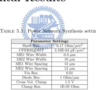
Table 5.1: Power Network Synthesis setting
Parameter Settings Sheet Res. 0.17 Ohm/µm2
CPERSQDIST 3.10E-04 pF/µm2
ME1 Wire Width 0.3 µm ME2 Wire Width 10 µm ME1 Wire Spacing 12 µm ME2 Wire Spacing 12 µm
Via Res. 0.01
Diode Res. 1 Ohm/µm Cross Vol. Clamp 1.5 V
Clamp Res. 1E-05 Ohm
In this chapter, experimental result of the proposed framework is presented. The entire framework is implemented with standard C++ language and compiled using g++ 4.1.2. Experiments are performed on an Intel XEON E5620 machine running at 2.4Ghz. GSRC benchmark [16] is used as input benchmarks. The number of power domains and driving voltage for each module are initially determined. Table 5.2 shows the detail of the input benchmarks. In Table 5.2, P. D. 2-Pin Net stands for number of 2-Pin nets between two power domains. I. Module stands for number of module within the voltage island and E. Module stands for number of external module voltage island connects to.
We reference UMC65 technology file and lists the value of parameters in Table 5.1. The discussion on experimental result discusses the effect of the power clamp placement to CDM level.
Chapter 6. Experimental Results 20
5.1
Analysis on Power Clamp Placement
To evaluate effectiveness of different power clamp placement methods, five floorplans are generated for each testcase. The floorplans are generated using default configuration which only considers area and HPWL of the netlist. Four power clamp placement methods are applied. The first method, uniform, adopts conventional approach which places power clamp with uniform spacing. The second method, periphery, places power clamp with uniform spacing only at the peripheral boundary of the device. The third approach, pin+periphery, places one power clamp next to each internal I/O pin and around the peripheral boundary. The fourth method, cluster+periphery, places power clamps based on clustering analysis and around the peripheral boundary.
Table 5.3 shows the performance of different power clamp placement methods. The uni-form method serves as the baseline approach to evaluate the other three methods. The purpose of periphery method is to achieve similar voltage distribution between VDD and VSS power domain when an external I/O pin is grounded. Table5.3shows that periphery method can achieve 95% to 103% of CDM level while using only 32% to 44% number of power clamps compared to the baseline approach. The pin+periphery method can ef-fectively improve CDM level of the design on all six designs by 1% to 14% compared to the baseline approach. However, redundant power clamps is placed for design with high density of internal I/O pins such as n200 and n300, the pin+periphery method requires an additional 44% and 19% number of power clamps.
To address the issue of redundant power clamp insertion, the cluster+periphery method aims to minimize the maximum distance from each internal I/O pin to its nearest power clamp. From Table 5.3, the cluster+periphery method achieves equivalent amount of improvement on CDM level while inserting average of 31% less power clamps compared to the pin+periphery method.
Chapter 6. Experimental Results 21 T able 5.2: Detail of the inp ut b enc hmarks. (P .D. stand s for n um b er of p o w er domains excluding chip p o w er domain. Net stands for n um b er of netlist. P .D. 2-Pin net stands for n um b er of cross p o w er domain 2-pin nets. In ternal I/O Pin stands for n um b er of in ternal I/O pins. I. Mo dule stands for n um b er of in ternal mo dules within the v oltage island. E. Mo du le stands for n um b er of external mo dules connected to the v oltage island.) P .D. Net P .D. In ternal P .D. 1 P .D. 1 P .D. 1 2-pin Net I/O Pin I. Mo dule E. Mo dule I. Mo dule E. Mo dule I. Mo dule E. Mo dule n10 10 2 118 25 9 1 9 1 6 NULL NULL n30 30 3 349 55 26 2 13 2 12 1 15 n50 50 3 485 123 43 2 28 2 18 2 25 n100 100 3 885 41 35 2 16 2 15 1 8 n200 200 3 1585 103 84 3 36 2 29 2 23 n300 300 3 1893 146 99 4 44 3 30 2 29
Chapter 6. Experimental Results 22 T able 5.3: Comparison on CDM lev el and n um b er of p o w er clamps using Uniform, P in+P eriph e ral and Cluster+P eripheral. (CDM stands for CDM lev el. C.# stands for n um b er of p o w e r clamps.) Pin Cluster Pin Cluster Uniform P eripheral + + Uniform P eripheral + + P eripheral P eripheral P eripheral P eripheral CDM C.# CDM C.# CDM C.# CDM C.# CDM C.# CDM C.# CDM C.# CDM C.# n10 1 1547 88 1396 30 1612 39 1612 39 n100 1 1068 76 1042 29 1077 63 1061 48 2 1598 90 1537 32 1590 41 1590 41 2 1428 81 1530 33 1881 66 1879 54 3 604 92 575 29 625 38 625 38 3 4835 73 4430 32 4776 65 4814 46 4 1861 94 1847 28 1800 37 1800 37 4 1797 77 1766 29 1971 63 1969 48 5 1770 99 1664 31 1750 40 1750 40 5 1847 83 1842 35 1904 69 1932 54 Max. 1861 94 1847 28 1800 37 1800 37 Max. 4835 73 4430 32 4776 65 4814 46 Min. 604 92 575 29 625 38 625 38 Min. 1068 76 1042 29 1077 63 1061 48 G.M. 1.00 1.00 0.95 0.32 1.01 0.42 1.01 0.42 G.M. 1.00 1.00 0.99 0.40 1.08 0.84 1.08 0.64 n30 1 755 91 686 35 809 61 810 55 n200 1 1423 78 1407 35 1501 116 1453 60 2 772 95 695 37 755 63 755 57 2 2144 81 1899 35 2059 116 1968 59 3 1189 95 1076 39 1194 64 1197 60 3 1830 75 1889 29 2221 108 2036 56 4 394 87 543 39 583 65 582 60 4 1387 82 1335 39 1623 119 1616 65 5 914 91 832 36 937 62 937 56 5 1289 80 1341 36 1585 113 1460 58 Max. 1189 95 1076 39 1194 64 1197 60 Max. 2144 81 1899 35 2221 108 2036 56 Min. 394 87 543 39 583 65 582 60 Min. 1289 80 1335 39 1501 116 1453 60 G.M. 1.00 1.00 0.99 0.41 1.10 0.69 1.10 0.63 G.M. 1.00 1.00 0.98 0.44 1.12 1.44 1.07 0.75 n50 1 511 88 508 35 537 78 540 57 n300 1 822 113 820 43 870 141 851 77 2 318 94 309 36 324 78 310 57 2 1061 120 1013 43 1291 140 1307 76 3 1435 94 1373 41 1521 84 1521 68 3 1219 113 1156 39 1305 136 1291 74 4 686 88 630 37 691 80 673 61 4 980 119 1008 44 1060 139 1051 81 5 946 88 1262 35 1603 78 1622 55 5 1104 123 1093 45 1191 142 1155 79 Max. 1435 94 1373 41 1603 78 1622 55 Max. 1219 113 1156 39 1305 136 1307 76 Min. 318 94 309 36 324 78 310 57 Min. 822 113 820 43 870 141 851 77 G.M. 1.00 1.00 1.03 0.41 1.14 0.88 1.13 0.66 G.M. 1.00 1.00 0.98 0.36 1.10 1.19 1.09 0.66
Chapter 6
Conclusion
In this work, we propose a CDM optimization framework that can be employed at design stage. During a CDM event, the instant that peak current occurs is when transistors are most vulnerable to a CDM event. To defend against a CDM event, we first propose a CDM simulation model that can be solved efficiently using static power analysis. While conventional methods on clamp placement generally insert redundant power clamps, we propose a clamp placement algorithm based on clustering analysis which can effectively minimize number of power clamps while achieving better CDM level.
Bibliography
[1] A. Amerasekera and C. Duvvury, ESD in silicon integrated circuits. John Wiley Sons, 2002.
[2] “ESDA.” Website. http://www.esda.org/.
[3] “JEDEC.” Website. http://www.http://www.jedec.org.
[4] M.-D. Ker, J.-J. Peng, and H.-C. Jiang, “ESD test methods on integrated circuits: an overview,” in The IEEE International Conference on Electronics, Circuits and Systems, vol. 2, pp. 1011–1014, 2001.
[5] C.-Y. Lin, T.-L. Chang, and M.-D. Ker, “Investigation on CDM ESD events at core circuits in a 65-nm CMOS process,” Microelectronics Reliability, vol. 52, no. 11, pp. 2627–2631, 2012.
[6] V. Shukla, N. Jack, and E. Rosenbaum, “Predictive simulation of CDM events to study effects of package, substrate resistivity and placement of ESD protection cir-cuits on reliability of integrated circir-cuits,” in IEEE International Reliability Physics Symposium, pp. 485–493, 2010.
[7] J. Lee, Y. Huh, J.-W. Chen, P. Bendix, and S.-M. Kang, “Chip-level simulation for CDM failures in multi-power ICs,” in Electrical Overstress/Electrostatic Discharge Symposium, pp. 456–464, 2000.
[8] J. Lee, K.-W. Kim, Y. Huh, P. Bendix, and S.-M. Kang, “Chip-level charged-device modeling and simulation in CMOS integrated circuits,” IEEE Transactions on Computer-Aided Design of Integrated Circuits and Systems, vol. 22, no. 1, pp. 67–81, 2003.
Bibliography 25 [9] Y. Huh, P. Bendix, K. Min, J.-W. Chen, R. Narayan, L.-D. Johnson, and S.-H. Voldman, “ESD-induced internal core device failure: new failure modes in system-on-chip (SOC) designs,” in International Workshop on System-on-Chip for Real-Time Applications, pp. 47–53, 2005.
[10] H. Qian, J.-N. Kozhaya, S.-R. Nassif, and S.-S. Sapatnekar, “A chip-level electro-static discharge simulation strategy,” in IEEE/ACM Proceedings of the International Conference on Computer Aided Design, pp. 315–318, 2004.
[11] J. Yang, Z. Li, Y. Cai, and Q. Zhou, “PowerRush: A linear Simulator for Power Grid,” in IEEE/ACM Proceedings of the International Conference on Computer Aided De-sign, pp. 483–487, 2012.
[12] Z. Zeng, T. Xu, Z. Feng, and P. Li, “Fast Static Analysis of Power Grids: Algorithms and Implementations,” in IEEE/ACM Proceedings of the International Conference on Computer Aided Design, pp. 488–493, 2012.
[13] C.-H. Chou, N.-Y. Tsai, Hao-Yu, C.-R. Lee, Y. Shi, and S.-C. Chang, “On the Pre-conditioner of Conjugate Gradient Method – A Power Grid Simulation Perspective,” in IEEE/ACM Proceedings of the International Conference on Computer Aided De-sign, pp. 494–497, 2012.
[14] Z. Li, R. Balasubramanian, F. Liu, and S. Nassif, “2011 TAU Power Grid Simu-lation Contest: Benchmark Suite and Results,” in IEEE/ACM Proceedings of the International Conference on Computer Aided Design, pp. 478–481, 2001.
[15] S. Lloyd, “Least Squares Quantization in PCM,” IEEE Transactions on Information Theory, vol. 28, no. 2, pp. 129–137, 1982.