國 立 交 通 大 學
顯示科技研究所
碩士論文
非晶與微晶矽鍺合金作為薄膜太陽能電池吸收層
之特性分析與最佳化
Characterization and Optimization of Amorphous
and Microcrystalline Silicon-Germanium Alloys as
Absorber Layers for
Thin-Film Solar Cell Applications
研究生:許宏榮 Hung-Jung Hsu
指導教授:蔡娟娟 教授 Prof. C.C. Tsai
非晶與微晶矽鍺合金作為薄膜太陽能電池吸收層
之特性分析與最佳化
Characterization and Optimization of Amorphous and Microcrystalline
Silicon-Germanium Alloys as Absorber Layers for
Thin-Film Solar Cell Applications
研究生:許宏榮 Student:Hung-Jung Hsu
指導教授:蔡娟娟 教授 Advisor:Prof. C.C. Tsai
國 立 交 通 大 學 顯示科技研究所 碩士論文 A ThesisSubmitted to Display Institute
College of Electrical Engineering and Computer Science National Chiao Tung University
In partial Fulfillment of the Requirements For the Degree of Master
In Display Institute July 2010
Hsinchu, Taiwan, Republic of China 中華民國九十九年八月
I
非晶與微晶矽合金作為薄膜太陽能電池吸收層之
特性分析與最佳化
研究生:許宏榮 指導教授:蔡娟娟 教授
國立交通大學顯示科技研究所
中文摘要
在本研究中,藉著改變氫流率、電漿功率以及製程氣體來研究非晶矽鍺與微 晶矽鍺之薄膜特性以及非晶矽鍺單接面太陽電池之轉換效率。製程氣體我們使用 矽甲烷(SiH4)、鍺甲烷(GeH4)以及氫氣,利用射頻電漿輔助化學氣相沉積系統 (PECVD)來沉積非晶矽鍺薄膜。由本篇實驗發現通入適當氫氣可提升光電導,而 鍺原子濃度亦影響光學能隙以及電性。電漿功率除了會影響薄膜沉積速率外同時 亦可提升電性。在元件的表現上可分為以下幾個部分:非晶矽鍺吸收層的厚度大 約在 150 nm 至 300 nm 之間為佳,過厚或過薄都會對效率有不良影響;較高的 沉積功率增強了對表面的離子轟擊效應因此讓元件填充因子下降;在 p/i 與 i/n 介面間加入一緩衝層可有效阻擋磷原子擴散至吸收層,使得界面品質改善;最後, 當我們將吸收層中的鍺含量做漸變的變化,元件有較大的開路電壓且效率可達 8.5 %。 在微晶矽鍺合金方面,當我們逐漸提升沉積時的放電功率可發現一個由非晶 矽鍺合金轉變到微晶矽鍺合金的區域,且越接近此轉變的區間,膜中的結晶範圍 越大。調整氫氣稀釋比例也可改變膜中的結晶率,但由光暗電導可發現此時的膜 大多為高度結晶。改變膜中的鍺含量會大幅影響微晶矽鍺薄膜的特性,氣態的鍺 濃度大約在 9 % 至 16 % 為最佳的區間,光暗電導的差距約為一至兩個數量 級。II
Characterization and Optimization of Amorphous and Microcrystalline Silicon-Germanium Alloys as Absorber Layers for
Thin-Film Solar Cell Applications
Master Student: Hung-Jung Hsu Advisor: Dr. Chuang-Chuang Tsai
Display Institute
National Chiao Tung University
Abstract
In this study, the effects of systematic variation in hydrogen dilution, RF power, gas phase ratio of germane (RGeH4) on the hydrogenated amorphous silicon germanium
(a-SiGe:H) and hydrogenated microcrystalline silicon germanium (μc-SiGe:H) alloys properties and a-SiGe:H single junction solar cell performance have been studied. The a-SiGe:H and μc-SiGe:H films were deposited from the mixture of SiH4, GeH4 , and H2
dilution by the plasma enhanced chemical vapor deposition (PECVD) system at 27.12 MHz. It has been found that hydrogen dilution plays an important role in the properties of films. Adequate hydrogen dilution ratio can improve the photo photosensitivity, but both higher and lower hydrogen dilution ratio deteriorates the film properties. Power density influences on the deposition rate and electronic properties. Photo conductivity is higher for films deposited at higher power density for all hydrogen dilution ratios. Dark conductivity is almost the same for films deposited at two different power densities for all hydrogen dilution ratios. The device performance is better for the cell deposited at 20 W then 30 W, which means that ion bombardment plays a more important role than i-layer film quality.
III
Acknowledgements
回顧這兩年來的點點滴滴,這篇論文能夠順利完成,的確要感謝許許多多的 人,有了你們的幫助,我才能在研究的路上稍有斬獲。 首先我要感謝的是 蔡娟娟教授,感謝老師帶我進入太陽能的研究領域,並 在研究的路上給予我許多幫助 ,尤其是當我在面臨抉擇時,老師不吝給我指引, 讓我思考得更周全能夠穩健的踏出下一步,非常感謝您! 其次我要感謝國錫學長,感謝學長在我的研究領域給予我非常多的指導與幫 助,從您身上我學到了不只是專業的知識,更多的是您讓我看到了一位專注在研 究與開發的工作者應有的典範,我會盡量以您為目標並繼續前進! 再來我要感謝建敏學長,在我碩一的時候您總是替我規畫好大大小小的事, 並且很願意撥空教我做實驗的方式甚至是和我溝通很多觀念,讓我能夠順著您的 腳步,慢慢的將自己轉換到一位研究生的角色,真的很感謝您,謝謝! 我要特別感謝振航學長,感謝您在管理實驗室上付出了相當多的努力,並謝 謝您總是給予我很多在研究上的幫助,每次跟您討論完都有一種踏實且安心的感 覺,尤其在論文修改方面也提供我很多寶貴的意見,希望接下來能在你身上學到 更多的東西! 接著我要感謝鵬鵬、柏翔、建亞等三位好朋友,感謝你們一直很照顧我,一 起做實驗量測討論報告改進打球唱歌的日子真是令人懷念,我覺得你們真是優秀 的一群,相信你們不管到哪裡都會表現得很出色的,希望我們能一直保持聯絡! 感謝辛瑋學長時常提點我許多做人的道理,您成熟、不屈不撓又穩重是我要 學習的目標,和您打球很開心;感謝彥棠學長在研究上給予我的幫助,總是讓我 能夠多思考一個問題不同的面向;感謝碩一的各位,智凱、怡萍及奕文,感謝你IV 們時常主動的幫我們準備實驗的材料,讓我們能專心在研究上,並且讓實驗室氣 氛更溫馨和諧;感謝世益、伍佰、琇文、明哲提供了我在實驗上的幫助,也讓實 驗室一直存在歡笑;感謝威豪、達欣、芳弘三位學長為實驗室打下良好的基礎, 並且教導我實驗的技巧,讓我能夠很快的熟悉各種機台的操作,有你們在的實驗 室總是充滿歡笑聲;感謝慶能、煥之、淑玲、鈞銘等學長姐在實驗上給予的協助, 希望有機會能再跟你們打個球敘敘舊;感謝奇美能源的前輩們,讓我學到很多開 發元件的邏輯跟技巧,特別感謝育華在實驗及規劃方面給我的協助,讓我學到很 多;感謝田仲豪老師在光學理論上給我的指引;感謝林怡欣老師精彩的講課讓我 有幸能學會一些有關光學理論的概念,並且感謝您在我面臨抉擇的時候不吝給予 我建議,非常感謝您! 感謝口試委員張正陽教授、陳方中教授、冉曉雯教授在百忙之中撥冗前來參 與口試並提供許多寶貴意見使論文能夠更臻於完善。 此外我還要感謝奈米中心的何惟梅小姐、林聖欽先生、黃國華先生,優貝克 的陳江耀以及張智皓先生,謝謝你們在實驗上給予我各種幫忙。也感謝光電所的 助理張欣恆小姐、古明嬿小姐、張雅惠小姐以及童雅玲小姐在行政業務上幫了我 許多忙。 我要感謝一直以來陪伴在我身邊的宜蓉,妳是最了解我的人,當我疲累時總 是支持著我的內心,還要時常包容我的孩子氣,很多事情多虧了妳才讓我做出正 確的選擇,感謝妳陪我完成了各種大大小小的事,我會變得更成熟的,謝謝妳! 最後,我要感謝我的父母親 許家豪先生、黃鈺雯女士,感謝您們一直以來 都尊重我的想法,傾聽我所遇到的困難並且給我很多的關懷,讓我能順利完成碩 士學業,希望我能夠早日成為一個獨當一面的人,謝謝你們!
V
List of Tables
Table 3.1 Vibration frequencies of SiHx(x=1~3) in a-Si:H [33] ... 20 Table 4.1 Illuminated J-V parameters of a-Si1-xGex:H single junction solar cells
VI
List of Figures
Fig 1.1 The change in the global energy composition until 2050/2100 ... 1
Fig 1.2 The progress of the best research-cell conversion efficiencies ... 2
Fig 1.3 Absorption coefficient, α, versus Photon energy for a-Si:H, μc-Si:H and c-Si ... 5
Fig 1.4 Schematic diagram of a single junction a-Si:H p-i-n solar cell structure. ... 6
Fig 2.1 Band diagram and sketch of (a)a p-n and (b)a p-i-n cells[4] ... 10
Fig 2.2 The atomic structure of (a) crystalline silicon (b) hydrogenated amorphous silicon and (c) hydrogenated amorphous silicon germanium alloy. ... 11
Fig 2.3 Schematic representation of the rf PECVD system. ... 13
Fig 3.1 Photo energy (ħ𝛚) as function of the 𝛂ħ𝛚 and the tauc band gap 17 Fig 3.2 Micro-Raman spectrometer composed of an He-Ne laser source, a microscope, a notch filter, a grating and a CCD camera [26] ... 18
Fig 3.3 Raman spectrum of a μc-Si:H sample ... 19
Fig 3.4 Schematics of the conductivity measurement ... 21
Fig 3.5 Schematic of air mass ... 22
Fig 4.1 (a) The deposition rate (b) The bonding intensity ratio, as a function of RH2 for three different RGeH4 at 8.3, 11.1, 16.7% ... 26
VII
different RH2 = 0-3 at RGeH4 = 8.3% ... 27
Fig 4.3 The dependence of photoconductivity and dark conductivity of a-Si1-xGex:H alloys on RH at various Xg ... 28
Fig 4.4 Dependence of the photo-to-dark conductivity ratio with hydrogen dilution ratio. ... 28 Fig 4.5 The dependence of optical band gap of a-Si1-xGex:H alloys on RH2
at various RGeH4 ... 29
Fig 4.6 (a) Enhancement factor and (b) Ge content in a-Si1-xGex:H alloys
as a function of RH for three various Xg at 8.3, 11.1, 16.7% ... 30
Fig 4.7 Hydrogen content as a function of hydrogen dilutiob ratio at
different three germane concentrations. ... 31 Fig 4.8 Dependence of the photo-conductivity (σph) and dark-conductivity
(σd) with hydrogen dilution ratio ... 32
Fig 4.9 Illuminated J-V characteristics of 216-nm-thick a-Si1-xGex:H single
junction solar cells prepared with one or two buffer layer. ... 34 Fig 4.10 QE spectra of a 216-nm-thick a-Si1-xGex:H single junction solar
cell under zero bias and -0.5 V bias. ... 35 Fig 4.11 Illuminated J-V characteristics of a-Si1-xGex:H single junction
solar cells with i layer prepared with 20 W and 30 W. ... 36 Fig 4.12 Illuminated J-V characteristics of a-Si1-xGex:H single junction
solar cells with different i layer thickness (180 nm and 226 nm). .. 38 Fig 4.13 Illuminated J-V characteristics of a-Si1-xGex:H single junction
solar cells prepared with different i layer thickness ... 39 Fig 4.14 Dependence of VOC, JSC, FF and Efficiency of a-Si1-xGex:H single
VIII
Fig 4.15 Illuminated J-V characteristics of 216-nm-thick a-Si1-xGex:H single
junction solar cells with different combination of back contact material. ... 41 Fig 4.16 Illuminated J-V characteristics of 216-nm-thick a-Si1-xGex:H single
junction solar cells post-annealed at various temperature (TS= 145 O
C, 150 OC, 155 OC, 160 OC). ... 43 Fig 4.17 Dependence of VOC, JSC, FF and Efficiency of a 216-nm-thick
a-Si1-xGex:H single junction solar cell on post-annealing
temperature. ... 43 Fig 4.18 Illuminated J-V characteristics of a-Si1-xGex:H single junction
solar cells prepared with constant and graded GeH4 concentration.
45
Fig 4.19 Illuminated J-V characteristics of a-Si1-xGex:H single junction
solar cells prepared with constant and different graded GeH4
concentrations. ... 46 Fig 4.20 Raman scattering spectra for μc-Si1-xGex films deposited on bare
glass at fixed germane concentration (RGeH4) with various power
ranging from 100 W to 600 W. ... 48 Fig 4.21 Dark conductivities (solid symbols) and photo conductivities (open
symbols) as a function of discharge power. ... 49 Fig 4.22 XRD spectra of μc-Si1-xGex films deposited on bare glass at fixed
germane concentration (RGeH4) with various power ranging from
100 W to 600 W. ... 50 Fig 4.23 Raman scattering spectra of μc-Si1-xGex films deposited on bare
IX
% to 98.9 %. The other deposition parameters were kept
unchanged. ... 51 Fig 4.24 Dark conductivities (solid symbols) and photo conductivities (open
symbols) as a function of hydrogen dilution ratio (RH2). ... 52
Fig 4.25 Raman scattering spectra of μc-Si1-xGex films deposited on bare
glass at different germane concentrations (RGeH4) ranging from 9.1
% to 33.3 %. The μc-Si:H film is also shown for comparison. ... 53 Fig 4.26 Dark conductivities (solid symbols) and photo conductivities (open
symbols) as a function of germane concentration (RGeH4). ... 54
Fig 4.27 Raman scattering spectra of μc-Si1-xGex films deposited on bare
glass at different germane concentrations (RGeH4) ranging from 3.8
% to 16.7%. ... 55 Fig 4.28 Dark-conductivities (solid symbols) and photo-conductivities (open symbols) as a function of germane concentration (RGeH4). ... 56
X
Contents
中文摘要... I Abstract ... II Acknowledgements ... III List of Tables ... V List of Figures ... VI Chapter 1 Introduction ... 1
1.1 Global Warming and Energy Resource Problem ... 1
1.2 Introduction to Photovoltaic (PV) Technology... 2
1.2.1 Current Development of PV Technology ... 2
1.2.2 Thin Film Solar Cell Technology ... 3
1.2.3 Si Thin-Film Solar Cell ... 5
1.3 Motivation ... 7
Chapter 2 Literature Review ... 8
2.1 Introduction ... 8
2.2 P-i-n Structure of Silicon Based Solar Cell ... 9
2.3 Hydrogenated Amorphous Silicon ... 10
2.3.1 Material Properties ... 10
2.3.2 Stabler-Wronski Effect ... 12
2.3.3 Hydrogenated Amorphous Silicon-Germanium Alloys ... 12
2.4 Radio-Frequency Plasma-Enhanced Chemical Vapor Deposition ... 13
XI
2.5.1 Material Properties ... 15
2.5.2 Hydrogenated Microcrystalline Silicon-Germanium Alloys ... 16
Chapter 3 Experimental Details ... 17
3.1 Material Characterization... 17
3.1.1 Reflection-Transmission Spectroscopy ... 17
3.1.2 Raman Spectroscopy ... 17
3.1.3 Fourier Transform Infrared Spectroscopy (FTIR) ... 19
3.1.4 X-Ray Diffraction (XRD) ... 20
3.1.5 I-V Measurement ... 20
3.2 Solar Cell Characterization ... 21
3.2.1 AM 1.5 Light Source ... 21
3.2.2 Current-Voltage Characteristics ... 23
3.2.3 Quantum Efficiency ... 24
Chapter 4 Results and Discussions ... 25
4.1 Deposition and Characterization of a-SiGe Thin-Films ... 25
4.1.1 The Effect of Hydrogen Dilution on Deposition Rate and Film Quality 25 4.1.2 The Effect of Hydrogen Dilution on Conductivity Properties ... 27
4.1.3 The Effect of Hydrogen Dilution on Optical Bandgap and Ge Atom Concentration ... 29
4.1.4 The Effect of RF Power on Film Quality ... 31
4.2 a-SiGe:H Single Junction Solar Cell Optimization ... 32
4.2.1 Effect of Buffer Layer on Cell performance ... 32
4.2.2 RF Power Effect on cell performance ... 35
XII
4.2.4 Layer Thickness Variation with Elevated Ge Incorporation ... 38
4.2.5 Back Contact Comparison ... 40
4.2.6 Anneal Temperature Optimization ... 42
4.2.7 Bandgap Engineering ... 44
4.2.8 n-layer Thickness Variation ... 46
4.3 Deposition of μc-SiGe:H Thin-Film and Performance of Solar Cells ... 47
4.3.1 Effect of RF Power on Film Quality ... 47
4.3.2 Effect of Hydrogen Dilution on Conductivity ... 50
4.3.3 Effect of GeH4 Concentration on Conductivity ... 52
Chapter 5 Conclusions ... 57
Chapter 6 Future Works ... 59
1
Chapter 1 Introduction
1.1 Global Warming and Energy Resource Problem
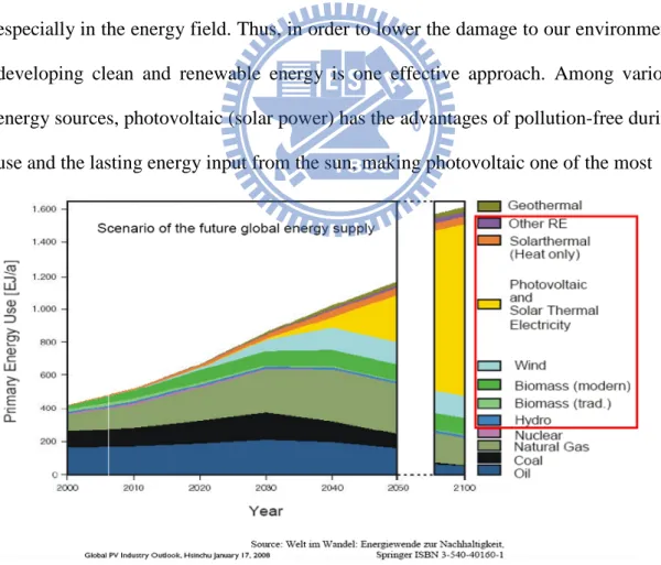
The global warming has already caused many worldwide disasters including floods, droughts, and the related problems like contagions and famine. Based on many research groups’ investigations, such as Intergovernmental Panel on Climate Change (IPCC), there is an apparent relationship between the carbon dioxide concentration and global temperature. The biggest source of carbon dioxide is the utilization of fossil fuel, especially in the energy field. Thus, in order to lower the damage to our environment, developing clean and renewable energy is one effective approach. Among various energy sources, photovoltaic (solar power) has the advantages of pollution-free during use and the lasting energy input from the sun, making photovoltaic one of the most
Fig 1.1 The change in the global energy composition until 2050/2100
2
German Advisory Council on Global Change (WBGU), solar power will be one of the highest-growing and the dominant energy resource in the future 100 years.
1.2 Introduction to Photovoltaic (PV) Technology
1.2.1 Current Development of PV Technology
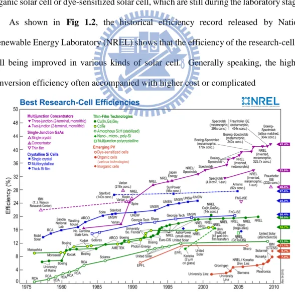
There are three generations of solar cells. The first generation is silicon (Si) wafer-based solar cell, which is with higher conversion efficiency but higher costs. The second generation is thin film solar cell, which is with lower costs as well as lower conversion efficiency. The third generation is solar cell with new materials such as organic solar cell or dye-sensitized solar cell, which are still during the laboratory stage.
As shown in Fig 1.2, the historical efficiency record released by Nation Renewable Energy Laboratory (NREL) shows that the efficiency of the research-cell is still being improved in various kinds of solar cell. Generally speaking, the higher conversion efficiency often accompanied with higher cost or complicated
3
fabrication process. The goal of grid-parity can only be achieved when the cost per watt is low enough compared to current fossil fuel.
Among various kinds of solar cell technologies, the most common solar cell is a crystalline silicon (c-Si) p-n junction. The Si atoms in this type are periodically arranged. High efficiency c-Si solar cell needs high quality and purity wafer, making the cost become higher. Also, the optical absorption coefficient of c-Si solar cell is low since Si is indirect band-gap material, which means the thickness should be thick enough to absorb photons. Once the price of c-Si rises, this high material consumption must increase the total cost of solar cell fabrication.
Compared to c-Si solar cell, thin-film solar cell technology is currently developed to reduce the amount of light absorbing material. Also, it is carried out at lower temperature, making it possible to deposit on cheaper or flexible substrates such as glass or plastic substrate. In addition to low cost and flexibility, thin film solar cell technology has advantages including lighter weight and ease of integration compared to wafer silicon. Due the above benefits, thin-film solar cell is a promising category of solar cells in the energy field.
1.2.2 Thin Film Solar Cell Technology
There are several categories in thin film solar cell technology including Si thin film, cadmium telluride (CdTe), copper indium selenide/ copper indium gallium selenide (CIS/CIGS), and Organic/polymer solar cell. The following are some introduction and characteristics about these thin film solar cells:
CdTe solar cells: With an optimal band-gap of 1.44 eV, CdTe is an efficient light-absorbing material for thin film cells. The cell thickness of nearly one micron is
4
enough to absorb photons, therefore, the material costs is significantly reduced. Efficiencies close to 10% have been achieved in commercial modules by Solar Cells Inc. However, the toxicity of CdTe-based solar cell on health and the environment is still a concern.
CIS/CIGS solar cells: These semiconductors are attractive materials due to their high optical absorption coefficient and versatile optical and electrical characteristics so that they can be manipulated to fit the needs for device. The best efficiency of CIGS solar cell has achieved 19.9% in 2008 [1]. By using optical concentrator or multi-junction tandem solar cell, higher efficiencies (>30%) can be obtained. But the manufacturing costs of CIGS solar cells are high when compared to amorphous silicon (a-Si) solar cells.
Organic/polymer solar cell: These devices don’t rely on built-in electric field like inorganic solar cells. The active layer consists of two materials, one acts as an electron donor and the other as an acceptor. The efficiencies of organic/polymer solar cell has quickly improved in recent years and the best one is 6.77% [2]. But the stability and excitation diffusion length should be enhanced in the future.
Si thin film solar cells: Si is the top two abundant element in earth's crust (only less than oxygen), and it makes up 25.7% of the crust by mass. That is the reason why Si-based solar cells are the most well-studied alternative energy method. Meanwhile, thin-film silicon solar cells such as hydrogenated amorphous silicon (a-Si:H) can be scaled to large area and deposited on various kind of substrates so that it is a promising material in the energy field. Furthermore, the multi-junction technology
5
based on the concept of spectrum splitting can also be applied to combine a-Si:H with hydrogenated microcrystalline silicon (μc-Si:H) solar cells to enhance absorption. Triple stack a-Si:H/μc-Si:H/μc-Si:H achieved module efficiency of up to 12% with much less photo-degradation [3]. Our group also focuses on this Si thin film solar cells.
1.2.3 Si Thin-Film Solar Cell
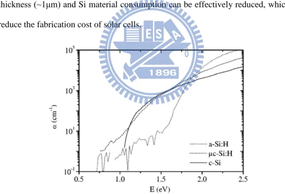
Si thin-film solar cells consists of a-Si based solar cells including amorphous silicon germanium (a-SiGe) and μc-Si based solar cells including microcrystalline silicon germanium (μc-SiGe). Compared to c-Si solar cell, the light absorption coefficient of thin film Si materials is much higher, as shown in Fig 1.3. Thus, the thickness (~1μm) and Si material consumption can be effectively reduced, which can reduce the fabrication cost of solar cells.
Fig 1.3 Absorption coefficient, α, versus Photon energy for a-Si:H, μc-Si:H and c-Si
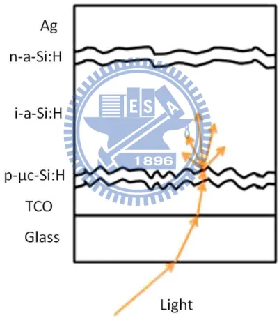
Silicon based thin-film solar cells can be fabricated in two configurations: p-i-n or n-i-p. We focus on p-i-n structure in this thesis, as shown in Fig 1.4. In this configuration, light enters from the p-layer side. The internal electric field is built up by
6
the Fermi level difference between p- and n-layer. When light incidence, electron-hole pairs are created in the intrinsic microcrystalline silicon layer (i-layer), which is the “photon absorption” process. Then, “charge separation” happens because of the internal electric field. During the transportation process, “charge recombination” occurs due to defects in the films. Finally, those charges transported longer enough will be collected by the electrodes. “Absorption, transportation, and collection” are the working mechanism for solar cell to convert light to electricity.
Fig 1.4 Schematic diagram of a single junction a-Si:H p-i-n solar cell structure.
There are several advantages of choosing a-Si:H based material as an absorber materials. First, due to the direct band-gap property, a-Si:H solar cell has higher optical absorption coefficient in visible spectrum. Also, the manufacturing method of a-Si:H is
7
mature and the cost is low. Besides, thin-films can be deposited on glass, metal or plastic substrates, which extends the application field of thin-film solar cells. But the serious light degradation is the main problem that should be improved.
The structure of μc-Si:H is between a-Si and c-Si, there are some crystalline parts incorporate into amorphous network. Because of such structure, μc-Si:H also possesses the advantages of a-Si:H such as high optical absorption coefficient and low cost. Furthermore, because the presence of crystalline phase, the light degradation of μc-Si:H is much less than that of a-Si:H.
The combination of a-Si:H and μc-Si:H tandem solar cell is a fascinating structure, because the absorption range are wide to cover most visible light spectrum. For a-Si:H, the absorption peak is toward short wavelength; for μc-Si:H, the absorption peak is toward long wavelength. Thus, combination of these two type solar cells could achieve a substantial increase of conversion efficiency due to broader light spectrum absorption.
1.3 Motivation
In order to enhance the conversion efficiency as well as to upgrade the performance per cost of silicon solar cell, this series of experiments investigates the characteristics of thin film material. We attempt to understand which material properties could improve the conversion efficiency and endeavor to manipulate these material properties by controlling appropriate process parameters. Consequently, a series of experiment on silicon thin film solar cell have been done in this thesis.
8
Chapter 2 Literature Review
2.1 Introduction
In 1905, the photoelectric effect was explained by Elbert Einstein. The explanation relies on ideas from quantum theory. Light is made up of a pack of photons, the photon energy depends only on the frequency (or wavelength) of light. When the wavelength of light is smaller than a threshold value (usually blue or ultraviolet light) then radiating at the surface of a metal, the electrons will absorb enough energy to escape completely. The escaping electrons are called photoelectrons. Because the work function of a metal is as high as 3 to 5 eV, so the maximum conversion efficiency of bounded electrons to photoelectrons is lower than 1%. This phenomenon is called as photoelectric effect and cannot be explained by wave theory, that is, the escape capability of bounded electrons depends on the energy of light, not on the intensity of light.
Generally speaking, the energy of photons in visible spectrum is sufficient to excite electrons to higher energy levels where they are easier to move, but the excited electrons will quickly relax back to their ground states. In photovoltaic devices, there is a built-in electric field which can separate photo-generated carriers away and extract them to external circuit. The extra energy of excited electrons generates a potential difference which drives these electrons to external load and does electrical works. This phenomenon is the photovoltaic effect.
9
2.2 P-i-n Structure of Silicon Based Solar Cell
There are three major mechanisms responsible for the collection of photo-generated carriers in p-n diode photovoltaic:
1. The drift current of holes and electrons in depletion region. 2. The diffusion current of minority carriers in n-type neutral region 3. The diffusion current of minority carriers in p-type neutral region
In typical mono-crystalline and poly-crystalline silicon p-n diode photovoltaic, the contribution of photo-generated carriers in depletion region is trivial due to the width of this region is too thin compared to the diffusion length of minority carriers. The main current of mono-crystalline and poly-crystalline solar cells is the diffusion current in the neutral region. The absorption coefficient of amorphous silicon is about two orders higher than crystalline silicon, the material needed in amorphous silicon thin film solar cells is 1% of crystalline silicon solar cells needed. However, amorphous silicon is a defective material. The diffusion lengths are so short in doped a-Si, the undoped region is needed to extend the thickness which photons can be absorbed effectively. The thin p-layer and n-layer create the built-in field which drives the charges to separate. In the p-i-n structure photo-carriers are collected primarily by drift rather than by diffusion.
10
Fig 2.1 Band diagram and sketch of (a)a p-n and (b)a p-i-n cells [4]
2.3 Hydrogenated Amorphous Silicon
The use of amorphous silicon can be retraced to 1965 as films of ‘silicon from silane’ deposited in a radio frequency glow discharge [5].Ten years later, Walter Spear and Peter LeComber reported that amorphous silicon had semiconducting properties. The conductivity of amorphous silicon can be manipulated by several orders of magnitude by adding some phosphine or diborane into the gas mixture [6]. One year later, Carlson and Wronski announced that they had made the first experimental a-Si:H solar cell at the RCA laboratory in 1976 [7]. The discovery of a-Si:H open a new era to thin film silicon solar cells and related technologies.
2.3.1 Material Properties
Hydrogenated amorphous silicon (a-Si:H) is the non-crystalline allotropic form of silicon. It can be deposited as thin film onto a variety of substrates at low temperatures. Silicon is a four-fold coordinated atom that is normally tetrahedrally bonded to four neighboring silicon atoms. In crystalline silicon this tetrahedral structure is continued
11
over a large range, forming a well-ordered lattice (crystal), as shown in Fig 2.2 (a). In amorphous silicon this long range order is not present and the atoms form a continuous random network. Not all the atoms within amorphous silicon are four-fold coordinated. Due to the disordered nature of the material, some atoms have unpaired electron, which is called dangling bonds. These dangling bonds present as defects or voids in the silicon random network, which cause anomalous electrical behavior.
Fig 2.2 The atomic structure of (a) crystalline silicon (b) hydrogenated
amorphous silicon and (c) hydrogenated amorphous silicon germanium alloy.
If desired, the material can be passivated by hydrogen which bonds to the dangling bond to reduce the dangling bond density by several orders of magnitude. This phenomenon makes amorphous silicon a useful material that the conductivities can be
12
manipulated by several orders of magnitude. In general, there exists about 10 at.% hydrogen in hydrogenated amorphous silicon thin film. Hydrogenated amorphous silicon has a sufficiently low amount of defects to be used within devices. However, the hydrogen is unfortunately associated with light-induced degradation of the material, termed the Staebler-Wronski effect.
2.3.2 Stabler-Wronski Effect
Electrical properties of amorphous silicon would be changed under long time light exposure. This phenomenon is well-known as Staebler-Wronski Effect discovered by D. L. Staebler and C. R. Wronski in 1977 [8]. Weak bonds in amorphous silicon like dihydride, trihydride bonds and cluster of Si-H may be broken and result in the formation of dangling bonds by long time illumination of light. When the defect density of dangling bonds increases, the lifetime of photo-generated carriers reduces. Due to the strong recombination loss through the localized states formed by the dangling bonds in amorphous silicon network, the conversion efficiency degraded severely in a-Si:H based solar cells [9-10].
However, an essential feature of light-induced effects on a-Si:H film and solar cell can be reversible by annealing above 150℃. The performance of stabilized a-Si:H solar cells is 70 to 85% of their initial efficiency depends on the quality of a-Si:H film. This light-induced degradation is the major disadvantage of amorphous silicon as a photovoltaic material.
2.3.3 Hydrogenated Amorphous Silicon-Germanium Alloys
Amorphous silicon alloys are widely used in thin film solar cell technologies, such as a-Si1-xGex. Structure of amorphous silicon germanium alloy is shown in figure Fig
13
2.2 (c). Incorporation of germanium adds extra freedom to controlling the properties
of the material. Increasing concentration of germanium in the alloy narrows the electric gap between conduction and valence band (called bandgap) and also potentially increases the light absorption coefficient and extends the absorption range of the solar spectrum. However, the electric properties as a semiconductor (mainly electron mobility), are negatively affected by the increasing content of germanium in the alloy, due to the increased disorder in the atomic network.
One advantage is that a-Si and its alloys can be deposited at very low temperatures (~200℃). This allows for deposition not only on glass, but plastic as well, making it a candidate for a roll-to-roll processing technique. Another advantage is that a-Si can be deposited over large areas by PECVD.
2.4 Radio-Frequency Plasma-Enhanced Chemical Vapor
Deposition
Plasma-enhanced chemical vapor deposition (PECVD) is a common technique
14
used for the manufacturing of most microelectronic devices. The deposition of hydrogenated films at lower temperatures requires a source of energy to dissociate SiH4
and GeH4 and this is the role of plasma. This is done by collisions with electrons, which
originates as secondary electrons in the plasma to acquire their energy by acceleration in an electric field. The growth of an a-SiGe:H and μc-SiGe:H film is accomplished by attaching reactive particles of dissociated silane and germane molecules, called radicals, to the surface, as sketched in Fig 2.3.
Most reactors have been designed in diode configuration in which plasma is confined between two parallel electrodes. Despite being a relatively simple reactor, there are many variables in the deposition process which must be controlled to give good material quality. The gas pressure determines the mean free path for collisions of the gas molecules and influences whether the reactions are at the growing surface or in the gas. The gas flow rate determines the residence time of the gas species in the reactor. The rf power control the rate of dissociation of the gas and therefore also the film growth rate. And the substrate temperature of the substrate controls the chemical reactions on the growing surface.
In the dissociation process, gas molecule will be decomposed into many kinds of neutral radicals or ions. Among these radicals and ions, there are two radicals that possess higher sticking coefficients than other radicals and they would incorporate directly onto the hydrogen terminated surface without finding potential favorable growth site. Therefore, these radicals are usually formed voids in the film resulting in poor film quality. So, the presence of these radicals in the plasma should to be avoided.
15
2.5 Hydrogenated Microcrystalline Silicon
2.5.1 Material Properties
The definition of hydrogenated microcrystalline silicon (μc-Si:H), based on the study done by Schropp [11], is a two-phase material including amorphous part and crystalline part with crystal sizes smaller than 20 nm. As a contrast, polycrystalline silicon is a single crystalline phase with grain boundaries and the smallest crystal sizes larger than 20 nm.
With plenty of researches in the recent years, it is a common agreement that microcrystalline silicon material owns the best quality at the transition region from amorphous to crystalline (with 30% to 70% crystallinity, but strictly speaking, the term transition might be incorrect [12]). This is because the film in this region incorporates some volume fractions of crystals in amorphous networks, which have lowered light-induced degradation effect (also known as Stabler-Wronski Effect, SWE [13]) than hydrogenated amorphous silicon material but keeps reasonably high value of photosensitivity. Also, due to its amorphous nature, the absorption coefficient keeps high value.
For the formation of microcrystalline silicon, there are mainly three models related to the induction by atomic hydrogen:
1) Hydrogen etching model [14]: atomic hydrogen selectively etches away amorphous silicon.
2) Surface diffusion model [15]: exothermic recombination of atomic hydrogen on the surface locally provides sufficient energy for crystallization.
3) Chemical annealing model [16]: subsurface structural relaxation mediated by permeating atomic hydrogen gives rise to crystallization.
16
2.5.2 Hydrogenated Microcrystalline Silicon-Germanium Alloys
Hydrogenated microcrystalline silicon-germanium (μc-SiGe:H) alloys have been developed as a narrower variable bandgap material for multi-junction solar cells [17-18]. Due to the low absorption coefficient, μc-Si:H must be deposited about 1μm to 2μm thickness so that it can absorb enough photons. Thus, doping germanium into the microcrystalline structure is a way to elevate absorption coefficient, just like the concept of doping germanium atoms into a-Si:H network. However, alloying with germanium deteriorate the formation of crystallites and thus made the incubation layer thicker [19].From the recent study, μc-SiGe:H get some break through about film quality by M. Kondo’s group [20-21] in which they discover the film quality will only changed with germanium content in the film and the most suitable of germanium content is about 10 % to 20 %. Microcrystalline silicon germanium material with larger germanium content shown deteriorate photo response and may induce too much defects to hinder the transportation of charge carrier [22]. Moreover, other groups such as IPV also reported about the properties of μc-SiGe:H materials [23]. Until 2010, the highest reported efficiency of μc-SiGe:H single junction solar cells is 7.92 % with i-layer thickness less than 1μm [21], even higher than μc-Si:H solar cell with 2-μm-thick absorber layer. Thus, there is a great potential that the μc-SiGe:H will become the next candidate of bottom cell material.
17
Chapter 3 Experimental Details
3.1 Material Characterization
3.1.1 Reflection-Transmission Spectroscopy
The optical bandgap of thin film use UV/VIS/NIR spectrometers to measure transmission (T) spectra were carried out between 200 nm and 1.3 μm in the step of 2 nm. Calculating optical bandgap (Eg) has to use transmission spectra and thickness of
thin film from Eq. 3.1.
√𝛂ħ𝛚 = 𝐜�ħ𝛚 − 𝐄𝐨𝐩𝐭� (Eq. 3.1)
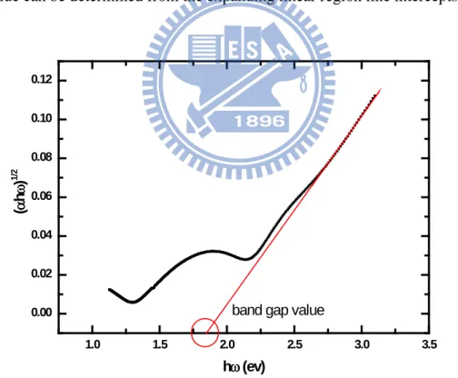
Fig 3.1 shows that the photo energy (ħω) as function of the √αħω. The band
gap value can be determined from the expanding linear region line intercepts a-axis.
Fig 3.1 Photo energy (ħ𝛚) as function of the √𝛂ħ𝛚 and the tauc band gap
3.1.2 Raman Spectroscopy
Raman spectroscopy is the fastest and the easiest experimental technique for the
1.0 1.5 2.0 2.5 3.0 3.5 0.00 0.02 0.04 0.06 0.08 0.10 0.12 (α h ω) 1/ 2 hω (ev)
18
measurement of the crystallinity. The Raman scattering effect, first reported by Raman and Krishna in 1928 [24], has been used to investigate the structural property of μc-Si:H nowadays. The theory of this method is given in literature [25]. The Raman apparatus used in this study was a HORIBA, Labram HR Raman microscope with an He-Ne laser source (633 nm).
Fig 3.2 Micro-Raman spectrometer composed of an He-Ne laser source, a microscope, a notch filter, a grating and a CCD camera [26]
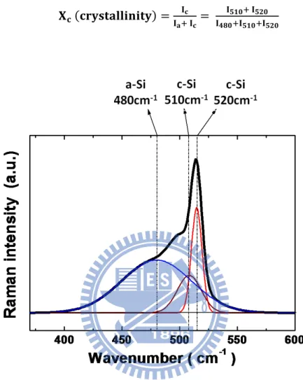
Fig 3.2 shows Raman spectrum of a μc-Si:H sample. In Raman spectroscopy, the
signal of a-Si:H appears as a broad peak at about 480 cm-1. The integrated intensity of this peak, Ia,is proportional to the volume fraction of a-Si:H in the film. The signal of
microcrystalline silicon appears as a narrow peak at 520 cm-1, which is the position of the transverse optic mode in mono-crystalline silicon. Another narrow peak occurs at about 510 cm-1 arising from the defective part of the crystalline phase (crystallites smaller than 10 nm [27], or to a silicon wurtzite phase [28] that result from twinning [29]). Therefore, the degree of crystallization can be considered proportional to the peaks at 510 cm-1 and 520 cm-1 and the Eq. 3.2 can be obtained by the deconvolution
19
and integration of Raman lines. Xc is a useful factor to quantify the crystallinity of
μc-Si:H thin films.
𝐗𝐜 (𝐜𝐫𝐲𝐬𝐭𝐚𝐥𝐥𝐢𝐧𝐢𝐭𝐲) =𝐈 𝐈𝐜
𝐚+ 𝐈𝐜 =
𝐈𝟓𝟏𝟎+ 𝐈𝟓𝟐𝟎
𝐈𝟒𝟖𝟎+𝐈𝟓𝟏𝟎+𝐈𝟓𝟐𝟎 (Eq. 3.2)
Fig 3.3 Raman spectrum of a μc-Si:H sample
3.1.3 Fourier Transform Infrared Spectroscopy (FTIR)
The incorporation of hydrogen in the amorphous silicon is beneficial because of the defect passivation. Infrared absorption spectroscopy is widely used to investigate the Si-Hx bonding configurations [30]. A peak around 2000 cm-1 is defined as the
stretching mode of the isolated Si-H bonds, and a peak around 2090 cm-1 is correlated with SiH2 and clustered (SiH2)n groups at internal surfaces of voids or grain boundries
20 Si have been identified as shown in Table 3.1.
The microstructure parameter R is defined as: 𝐑 = 𝐈𝟐𝟎𝟗𝟎
𝐈𝟐𝟎𝟎𝟎+𝐈𝟐𝟎𝟗𝟎 (Eq. 3.3)
where I2000 and I2090 are the integrated absorption strength of the peaks at 2000 cm-1 and
2090 cm-1 respectively. The ratio R is widely used to characterize the microstructure in the a-Si:H network. As the 2100 cm-1 contribution increases, the ratio R increases which is the sign of poor quality material.
Table 3.1 Vibration frequencies of SiHx (x=1~3) in a-Si:H [33]
Group Stretching Bending Rocking / Wagging
SiH 2000 630
SiH2 2090 880 630
(SiH2)n 2090~2010 890,945 630
SiH3 2014 950,860 630
3.1.4 X-Ray Diffraction (XRD)
X-Ray diffraction is a method to gain information about crystal structure, orientations and crystal defects [34] based on Bragg's equation. XRD analysis was carried out by Bede, D1 diffractometer with 2θ scan (Bragg-Brentano geometry) with an angle step of 0.1 ° and a signal collection time of 1 s. CuKα–radiation characterized with a wavelength of λ=1.542 Å ( ~8 keV) was initiated by a voltage of 40 kV and a current of 40 mA.
3.1.5 I-V Measurement
21
were deposited onto the film by thermal evaporation. Conductivity is calculated by
Eq. 3.4, where V and I are the bias voltage and measured current, respectively. The
volume of material contributing to conductivity is determined by the width (W), length (L), and thickness (t) of a cuboid located between the conducting contacts used to probe the sample in the Fig 3.4.
𝛔 = �𝐕𝐈� �𝐖𝐋� �𝟏𝐭� (Eq. 3.4) A prepared a-Si1-xGex:H film with silver contacts is show in Fig 3.4.
Photoconductivity was measured by AM1.5 light spectrum with power at 100 mw/cm2. For the amorphous silicon germanium film, the thickness is about 600 nm.
Fig 3.4 Schematics of the conductivity measurement
3.2 Solar Cell Characterization
The solar cell efficiency is measured by the solar simulator with a corrected AM 1.5 light source.
3.2.1 AM 1.5 Light Source
Solar radiation closely matches a black body radiator at 5,800 K. As the sunlight travels though the atmosphere, chemicals react with the sunlight and absorb certain
22
wavelengths. Perhaps the best known example is the stripping of ultraviolet light by ozone in the upper atmosphere, which drastically reduces the amount of short wavelength light reaching the Earth's surface. A more active component of this process is water vapor, which results in a wide variety of absorption bands at many wavelengths, while molecular nitrogen, oxygen and carbon dioxide add to this process. Atmospheric scattering also plays a role by removing higher frequencies from direct sunlight and scattering it about the sky. The greater the distance of atmosphere the sunlight travels through, the greater this effect, which is why the sky looks pink at sundown when the sunlight is traveling obliquely through the atmosphere.
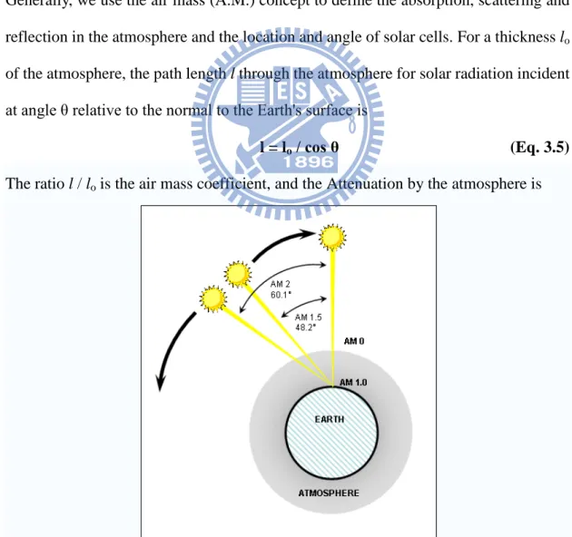
Generally, we use the air mass (A.M.) concept to define the absorption, scattering and reflection in the atmosphere and the location and angle of solar cells. For a thickness lo
of the atmosphere, the path length l through the atmosphere for solar radiation incident at angle θ relative to the normal to the Earth's surface is
l = lo/ cos θ (Eq. 3.5)
The ratio l / lo is the air mass coefficient, and the Attenuation by the atmosphere is
23 quantified by the air mass coefficient.
As shown in Fig 3.5, the spectrum outside the atmosphere, the 5,800 K black body, is referred to as "AM0", meaning "zero atmospheres". Cells used for space power applications, like those on communications satellites are generally characterized using AM0.
The spectrum after traveling through the atmosphere to sea level with the sun directly overhead is referred to as "AM1". This means "one atmosphere". Conveniently, silicon solar cells are not very sensitive to the portions of the spectrum lost in the atmosphere. Since solar cell development is concentrated in the United States, Europe and Japan, an AM number representing the spectrum at mid-latitudes is much more common. "AM1.5", 1.5 atmosphere thicknesses, corresponds to a solar zenith angle of 48°, and is almost universally used to characterize solar panels.
3.2.2 Current-Voltage Characteristics
The measurement of I-V characteristics is the primary method to evaluate solar cells performance. It is measured under AM 1.5 light source.
• The efficiency (η) is defined as the ratio of the maximum power generated by the device and the radiation power incident in the area of cell.
• The short-circuit current density (Jsc)is the maximum current density generated by
the device under light illumination.
• The open-circuit voltage (Voc) is the maximum voltage generated by the device
under light illumination.
• The fill factor (F.F.) is defined as a ratio of maximum power generated by the cell and the ideal power generated which is equal to Isc× Voc. This factor relate to the shunt resistance, series resistance and material quality in the device.
24
3.2.3 Quantum Efficiency
Spectral response provides the information about the working principle of solar cell. The Quantum efficiency is defined as
𝐐. 𝐄. = 𝐞 × 𝛗 (𝛌)𝐉𝐩𝐡(𝛌) (Eq. 3.6) where, Jph is the photo-generated current density per wavelength interval, e is the
elementary charge, and ψ is the number of photon per time, area, wavelength interval. Therefore, the quantum efficiency describes the probability that an incident photon generates a charge carrier pair which contributes to the photo current.
25
Chapter 4 Results and Discussions
4.1 Deposition and Characterization of a-SiGe Thin-Films
Hydrogenated amorphous silicon germanium and Hydrogenated microcrystalline silicon germanium were deposited using SiH4, GeH4 and H2 by radio frequency
(27.12 MHz) plasma enhanced chemical vapor deposition (PECVD) system. Doping layers were prepared by using diluted B2H6 or PH3 with SiH4 and H2. Prior to
depositing all the samples, NF3 and Ar were introduced to clean the chamber. Corning
Eagle2000 glass and c-Si wafer substrate were cleaned by KG detergent and RCA standard cleaning process, respectively. All the samples were deposited after a background pressure of 5 * 10-4 Pa was reached. In this study, a-SiGe:H and μc-SiGe:H alloys were prepared on 5cm x 5cm Corning Eagle 2000 glasses and 1.5cm x 1.5cm c-Si wafers. The films grew on glass substrate were used to analyze optoelectronic properties, and the films grew on c-Si wafer were used to determine the hydrogen bonding configuration by FTIR.
4.1.1 The Effect of Hydrogen Dilution on Deposition Rate and
Film Quality
Fig 4.1 (a) shows that the deposition rate drops drastically with increasing
hydrogen dilution ratio at different GeH4 concentrations. This is because hydrogen
radicals on the growing surface will enhance the etching effect. Hydrogen radicals will selectively break the weak Si-Si bond and leave a vacancy to give a chance to form a stronger bonding. Also, the concentration of SiH4 and GeH4 in H2 were lower
26
with increasing hydrogen dilution ratio. The deposition rate at different GeH4 concentration, however, shows no significant variation.
Fig 4.1 (b) shows the microstructure factors calculated by the signal of Si-H and
Si-H2 bonding configuration obtained from FTIR. The figure shows that when
hydrogen dilution ratio increases, the SiH2/SiH ratio drop and then may slightly rise
again. This indicates that hydrogen etching effect will improve film quality, but too much hydrogen will deteriorate the film quality. Furthermore, films deposited by higher GeH4 concentration will result in higher SiH2/SiH ratio. This is due to the films
incorporated with more Ge atoms will deteriorate the film quality.
Fig 4.1 (a) The deposition rate and (b) the bonding intensity ratio as a function of RH2 at different RGeH4 at 8.3 %, 11.1 % and 16.7%, respectively
0.0
0.2
0.4
0.6
0
2
4
6
8
0.0
0.3
0.6
R
GeH4= 16.7%
R
GeH 4= 11.1%
R
GeH 4= 8.3%
(b)
R
GeH 4= 8.3%
R
GeH 4= 11.1%
R
GeH 4= 16.7%
D
e
pos
it
ion R
a
te
(n
m
/s
)
(a)
I
SiH 2/
(
I
SiH 2+ I
Si H)
(a
.u
.)
H
2Dilution Ratio R
H 2(%)
27
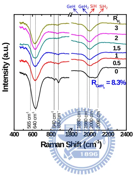
Fig 4.2 Fourier transform infrared spectra of a-Si1-xGex:H alloys with different
RH2 at RGeH4 = 8.3%
4.1.2 The Effect of Hydrogen Dilution on Conductivity Properties
Fig 4.3 shows that when hydrogen dilution ratio increased, the conductivities
raise about one order of magnitude, and the photo response increased, too. This should be due to the increasing of hydrogen etching ability which makes film quality become better. But the film quality gets worse when hydrogen dilution exceed a threshold value. This may be due to the severe gas phase reaction or the over etching, which produces more defects in the film and deteriorates film quality.
400
600
800
1800 2000 2200 2400
SiHGeH GeH2 SiH2
RH 2 3
R
GeH 4= 8.3%
2 1.5 1 0.5In
ten
si
ty (
a.
u
.)
Raman Shift (cm
-1)
0 1880 cm -1 1980 cm -1 2000 cm -1 2090 cm -1 890 cm -1 840 cm -1 640 cm -1 565 cm -128
Fig 4.3 The dependence of RH2 on photo-conductivity and dark-conductivity of
a-Si1-xGex:H alloys at three RGeH4
0
2
4
6
8
10
210
310
410
510
6R
GeH 4= 16.7%
σ
ph
/
σ
d
Ra
ti
o
H
2Dilution Ratio (R
H 2)
R
GeH 4= 8.3%
Fig 4.4 Dependence of the photo-to-dark conductivity ratio with hydrogen dilution ratio.
0
2
4
6
8
10
-1010
-910
-810
-710
-610
-5R
GeH 4= 8.3%
R
GeH 4= 11.1%
R
GeH 4= 16.7%
σ (
S
/c
m)
H
2Dilution Ratio R
H 229
4.1.3 The Effect of Hydrogen Dilution on Optical Bandgap and Ge
Atomic Concentration
Fig 4.5 and Fig 4.6 show that the relationship between hydrogen dilution and the
Ge content and also the bandgap. When we increase the hydrogen dilution the germanium content will also increase due to the more efficient dissociation of GeH4
than SiH4. This can be seen from the three GeH4 concentrations. Also, the
incorporation of Ge atom into the film will lower the bandgap of the material so that we can manipulate the bandgap of SiGe alloy by control the amount of hydrogen dilution, which is shown in Fig 4.5. There is another thing shown from Fig 4.5 that
Fig 4.5 The dependence of optical band gap of a-Si1-xGex:H alloys on RH2 at
various RGeH4
the bandgap drops drastically when hydrogen dilution between 0 and 2 and then
0
2
4
6
8
1.4
1.6
1.8
E
g(
e
V )
H
2Dilution Ratio R
HR
GeH 4= 8.3%
R
GeH 4= 11.1%
R
GeH 4= 16.7%
30
reaches a saturation value for three different GeH4 concentrations. Fig 4.7 shows
another effect that as hydrogen dilution increase the H content in the film decreased, which arise from the hydrogen facilitates the dissociation of GeH4 and strengthens the
hydrogen etching effect so that the Ge content is increased while H content is decreased.
Fig 4.6 (a) Enhancement factor and (b) Ge content in a-Si1-xGex:H alloys as a
function of RH2 for three RGeH4 at 8.3 %, 11.1 % and 16.7 %,
respectively. 0 1 2 3 4 5 6 0 10 20 30 40 0 1 2 3 4
G
e
C
o
n
te
n
t C
Ge(a
t.
%
)
H
2Dilution Ratio R
H 2R
GeH 4= 16.7%
R
GeH 4= 11.1%
R
GeH 4= 8.3%
R
GeH 4= 8.3%
R
GeH 4= 11.1%
R
GeH 4= 16.7%
(b)
E
n
h
a
n
c
e
m
e
n
t
F
act
o
r (
y)
(a)
31
0
2
4
6
8
10
0
5
10
15
20
GeH
4/(SiH
4+GeH
4)=8.33%
GeH
4/(SiH
4+GeH
4)=11.11%
GeH
4/(SiH
4+GeH
4)=16.67%
H
2C
o
n
te
n
t (a
t.
%
)
H
2Dilution Ratio (R
H 2) (%)
Fig 4.7 Hydrogen content as a function of hydrogen dilution ratio at different germane concentrations.
4.1.4 The Effect of RF Power on Conductivity
From Fig 4.8, the increase of rf power makes the photo conductivity rise and dark conductivity decrease. Also, the figure shows the same trend as above mentioned that when hydrogen dilution increase the deposition rate and bandgap decrease and reach a saturation region. The figure at bottom shows that the influence of hydrogen dilution to SiH2/SiH, GeH2/GeH ratio and power. As hydrogen dilution increase the
SiH2/SiH, GeH2/GeH ratio drop because hydrogen radicals will etch the growing
surface and also feed energy to make atoms find a binding site with lowest potential energy. Moreover, increase power can lower the SiH2/SiH and GeH2/GeH ratio this
can be explained by that it gives more energy to let atom diffuse on the growing surface and find a lowest energy binding site.
32
Fig 4.8 Dependence of the photo-conductivity (σph) and dark-conductivity (σd)
with hydrogen dilution ratio
4.2 a-SiGe:H Single Junction Solar Cell Optimization
Although we have made certain progress in cell performance, there are still some aspects needed to be improved for higher efficiency. Therefore, in this section, the improvement of a-SiGe single junction solar cell from a baseline to the latest result will be discussed. Besides, some possible issues that can cause efficiency improvement will also be disclosed here.
4.2.1 Effect of Buffer Layer on Cell performance
In this section, we replace original a-Si p-layer with undoped a-Si buffer layer and hypothesize that this change will increase JSC and FF. Then further increasing germane
concentration in gas phase from 11.1 % to 16.7 %, the characterized Ge content by XPS
75
80
85
90
1E-10
1E-8
1E-6
1E-4
0.01
20W
40W
R
GeH 4= 16.7 %
σ (
S
/c
m)
Hydrogen dilution ratio (%)
σd 30 W σph σd 40 W σph σd 20 W σph
30W
33
shows that the film deposited at 16.7% RGeH4 is composed of about 38 % Ge atom and
bandgap is 1.45 eV by Tauc plot [35].
From the former structure, the thin a-Si p-layer between a-Si p+ and a-SiGe i-layer formed a graded bandgap profiling, but doping boron also induce a large amount of defects in a-Si:H material; furthermore, when depositing i-layer, the substrate heating will provide enough energy to let boron diffuse into a-SiGe i-layer and decrease film quality. Therefore, inserting a buffer layer into p/i interface can resist boron diffusion and can eliminate the defects induced by doping boron which in turn improve the interface quality. Furthermore, the a-Si n-layer between i-layer and n+ layer may hinder charge carrier transport as well. So, by considering above, we made following two changes:
1. Replace a-Si p-layer with a-Si buffer layer
2. Replace both a-Si p-layer and a-Si n-layer with a-Si buffer layer.
Fig 4.9 shows the I-V curve comparison between cells with one p-layer replaced
by a buffer layer and two buffer layer replaced. Solar cells represent here were not post annealed. Cell structure with two buffer layers insertion is higher in efficiency than the cell with one buffer layer insertion due to the improved JSC and FF. Moreover, the short
circuit current density and therefore efficiency is higher than former structure, which can be explained by the improved interface quality by lowering the defect density and prevention of impurity diffusion. So we can conclude that cell with structure p+/b/i/b/n+ will present better cell performance than the former structure p+/p/i/n/n+.
Another interesting observation can be seen from Fig 4.10 is that quantum efficiency had been improved compared with the former one by the increased absorption in the whole spectrum. However, the absorption range still has no significant shift toward long wavelength region; despite that germanium content in the
34
film is about 38 %. The results conflict the general understanding that elevated germanium content will directly increase the absorption of long-wavelength region. The reason for below expectation absorption in long wavelength region is still not clear, and the possible reason maybe the diffusion length is shortened by the increased germanium content, so that the charge carrier excited by long wavelength photons will have larger chance to be recombined before collected by external circuit. So, if the hypothesis is correct, then further optimization of film thickness is needed for improvement of quantum efficiency, and other possible solutions are now under consideration.
Fig 4.9 Illuminated J-V characteristics of 216-nm-thick a-Si1-xGex:H single
junction solar cells prepared with one or two buffer layer.
0.0
0.2
0.4
0.6
0.8
0
5
10
15
20
p
+
/b/i/n
+
C
u
rr
en
t d
en
si
ty (
m
A
/cm
2)
Voltage (V)
VOC JSC FF η (V) (mA/cm2) (%) (%) p/b/i/n 0.65 15.6 55.0 5.60 p/b/i/b/n 0.65 16.0 58.0 6.00p
+
/b/i/b/n
+
35
Fig 4.10 QE spectra of a 216-nm-thick a-Si1-xGex:H single junction solar cell
under zero bias and -0.5 V bias.
4.2.2 RF Power Effect on cell performance
Remind that post-annealing will provide some energy to vibrate molecule and ease tension within material, increasing RF power also provide energy for molecule rearrangement. When depositing thin film, the dynamic balance is very important, for material relax itself while atom continuously deposit on growing surface. This process is more efficient compared with post-annealing. Therefore, elevate RF power will facilitate molecule diffusion on the growing surface and speed the deposition rate. Theoretically, higher RF power will improve film structure, but it also increase deposition rate so that the molecule might have no chance to diffuse due to the fast growth on growing surface. So, the preferable power is the result of dynamic balance between molecule relaxation and deposition rate.
Recall from previous result in Fig 4.8, when we elevate power from 20 W to 30 W, both photo and dark conductivity were improved nearly one order, as expected
36
with pervious discussion. But we notice one interesting thing from Fig 4.11 that cell with a-SiGe i-layer deposited at 20W has higher efficiency than cell deposited at 30 W. This observation can be understood by that although increasing RF power will facilitate film relaxation, but the film deposited at 30 W will suffer from stronger ion bombardment than film deposited at 20 W, thus create more defect throughout the material. And in turn lower the FF at higher power. So, we can conclude that the film quality is result of compromise of dynamic situation. Further optimization between 20 W and 30 W should be done in the future.
0.0
0.2
0.4
0.6
0.8
0
5
10
15
Power VOC JSC FF η (mV) (mA/cm2) (%) (%) 20 W 713 14.62 65.88 6.87 30 W 723 14.03 63.06 6.4020 W
C
u
rr
en
t D
en
si
ty
(mA
/c
m
2)
Voltage (V)
30 W
Fig 4.11 Illuminated J-V characteristics of a-Si1-xGex:H single junction solar
cells with i layer prepared with 20 W and 30 W.
4.2.3 Thickness Variation for p+/b/i/b/n+ Structure
In this section we want to further optimize i-layer thickness because we elevate germane concentration from previous 11.1 % to now 14.3 %, so that the proper film
37
thickness will change. Recall that in section 3.2.2 we have mentioned that the optimized thickness will change with Ge content in the film and also found that i-layer thickness of 200 nm will represent best cell performance for germanium concentration 11.11% in gas phase. Another difference from sec. 3.2.2 is structure, the former baseline is p+/p/i/n/n+, while after a serious experiments we found p+/b/i/b/n+ will represent better cell performance. Hence the proper i-layer thickness should be find out again.
The comparison of I-V curve between different i-layer thickness 180 nm and 226 nm are shown in Fig 4.12, and cell with thinner i-layer thickness present lower efficiency than cell with 226 nm thickness. Although shorten the i-layer thickness makes JSC become larger, but FF drops and compensate the increase of JSC, so total
efficiency is lower than thicker i-layer thickness. The reason of this result is not so clear because when thickness is thinned, charge carriers has higher possibility to be separated from the material before being recombined, which in turn cause larger JSC. However,
the drop of FF is unexpected and might be an experimental error. Therefore, further examine of film thickness is needed to find out an optimal thickness.
![Fig 3.2 Micro-Raman spectrometer composed of an He-Ne laser source, a microscope, a notch filter, a grating and a CCD camera [26]](https://thumb-ap.123doks.com/thumbv2/9libinfo/8756083.206933/32.892.141.760.330.701/micro-raman-spectrometer-composed-source-microscope-filter-grating.webp)
![Table 3.1 Vibration frequencies of SiH x (x=1~3) in a-Si:H [33]](https://thumb-ap.123doks.com/thumbv2/9libinfo/8756083.206933/34.892.125.762.467.749/table-vibration-frequencies-sih-x-x-si-h.webp)