國 立 交 通 大 學
電信工程學系
碩 士 論 文
10 位元 80 百萬赫茲導管式類比數位轉換器
和 CMOS 能階參考電路
10-Bit 80MHz Pipelined
Analog-to-Digital Converter and
CMOS Bandgap Reference Circuit
研究生:張 家 瑋
指導教授:洪 崇 智 教授
10 位元 80 百萬赫茲導管式類比數位轉換器
和 CMOS 能階參考電路
10-Bit 80MHz Pipelined Analog-to-Digital Converter and
CMOS Bandgap Reference Circuit
研 究 生:張家瑋 Student:Chia-Wei Chang
指導教授:洪崇智 教授 Advisor:Prof. Chung-Chih Hung
國 立 交 通 大 學
電 信 工 程 學 系 碩 士 班
碩 士 論 文
A Thesis
Submitted to Department of Communication Engineering College of Electrical Engineering and Computer Science
National Chiao Tung University in Partial Fulfillment of the Requirements
for the Degree of Master of Science in Communication Engineering January 2006 Hsinchu, Taiwan.
中華民國九十五年一月
10 位元 80 百萬赫茲導管式類比數位轉換器
和 CMOS 能階參考電路
研究生:張家瑋 指導教授:洪崇智 教授
國立交通大學
電信工程學系碩士班
摘要
高速類比數位轉換器是目前高效能系統,例如光纖通訊的前端接收器和資料 通訊連結系統中不可獲缺的主要電路。高速類比數位轉換器在設計上,需要考慮 如何將電路不匹配所造成的靜態(static)或動態(dynamic)的誤差如 DNL,INL 等誤差降低,以增加電路的解析度(resolutions)。此高速類比數位轉換器亦將 採用低電壓操作,已達到低功率消耗的標準。在設計上如何將高速,高解析度和 低功率消耗的優點集中在此類比數位轉換器,將是研究的重點之ㄧ。 一般而言,類比數位轉換器取樣頻率大於 1 GS/s 時,大多採用 Flash 架構 的轉換器。當解析度每增加 1 位元(Bit)時,電晶體的數目將增加 4~8 倍,造成 晶片面積和功率消耗增加,因此一般而言採用 Flash 架構的轉換器,其解析度普 遍都不會大於 6 位元。為了提高轉換器的解析度,可採用導管式(Pipeline)架構 的轉換器,此導管式轉換器主要是犧牲整體速度達到解析度的提升,因此可在速 度、解析度和晶片面積之間取得最佳化。解析度 10 位元、取樣頻率 80 MS/s 的 導管式類比數位轉換器(Pipelined ADC)將會在此研究中實現。 在此研究中,轉換器採用每一級 1.5 位元,串接八級,最後加上一級 2 位元 的子轉換器,實現 10 位元的解析度。一個 10 位元每秒取樣 80 百萬次操作電壓 1.8 伏特的導管式類比數位轉換器,在晶片中心(CIC)提供的台積電(tsmc)標準 0.18 微米製程中被設計與實現。論 文 中 , 低 功 率 消 耗 的 互 補 式 金 氧 半 能 階 參 考 電 路 (CMOS Bandgap Reference),將以晶片中心(CIC)提供的台積電(tsmc)標準 0.18 微米製程設計與 實現。此電路將電晶體偏壓在弱反轉層(weak-inversion region),使其產生取 代傳統雙載子(BJT)元件的電壓-電流關係式。此電路利用偏壓在弱反轉層電晶體 閘源極(VGS)間的壓差,產生正溫度係數的電壓,再加上負溫度係數的電壓,藉此 達到穩壓的效果。此電路以標準的CMOS製程實現,不需而外的製程輔助。
10-Bit 80MHz Pipelined Analog-to-Digital Converter and
CMOS Bandgap Reference Circuit
Student:Chia-Wei Chang Advisor:Prof. Chung-Chih Hung
Department of Communication Engineering National Chiao Tung University
Hsinchu, Taiwan
Abstract
High speed analog-to-digital converters (ADCs) and digital-to-analog converters (DACs) are very significant blocks of nowadays high-performance systems such as data communication links using multilevel signaling (e.g., PAM and QAM). The main issues in the design of high-speed ADCs include static and dynamic offset reduction, low supply-voltage operation, gain, and speed optimization. Design tradeoffs between power, speed, and chip area further tighten the design requirements.
For analog to digital conversion at sampling rates above 1 GS/s, typically flash converters are used. The resolution of these converters is limited because each extra bit would require 4 to 8 times more gate areas resulting in excessive power consumption. Generally speaking, flash converters are practically limited to 6 bits of accuracy. For lower speed, alternative architectures are widely available, such as pipelined converters which enable higher resolution and higher efficiency. In this research, a 10-bit 80 MS/s pipelined ADC will be presented.
The converter uses the 1.5 bit/stage architecture that cascodes eight stages. A 2 bit flash sub-converter in the last stage is utilized to achieve the 10-bit resolution. A 10 bits、80 MS/s and 1.8 V Pipelined ADC was designed and implemented by tsmc 0.18um process supported by CIC.
Also, a low power CMOS Bandgap Reference Circuit was designed and implemented by tsmc 0.18um process supported by CIC. The BJTs are replaced by the MOSFETs which operate in the weak-inversion region because the MOSFETs operating in the weak-inversion region have similar voltage-current relationship to the
BJTs. The bandgap reference circuit uses the different VGS voltage between two
MOSFETs operated in weak-inversion region to generate the voltage of positive temperature coefficient. We could get the stable reference voltage by combine the voltage of positive temperature coefficient with voltage of negative temperature coefficient. This circuit was designed in standard CMOS process without any other process.
誌謝
首先要感謝我的指導教授洪崇智老師在我兩年的研究生活中,提供良好的學 習環境,以及這段日子來對我的指導與照顧,並且在研究主題上給予我寬廣的發 展空間。同時我也要感謝碩士班兩年內曾經敎過我的每位老師,由於他們熱心的 教學,使我在短短的碩士班兩年內,學習如何設計、製作類比積體電路。此外要 感謝蘇育德教授、闕河鳴教授、陳信樹教授撥空擔任我的口試委員並提供寶貴意 見,使得本論文更為完整。還有,感謝國家晶片系統設計中心提供先進的半導體 製程,讓我有機會將所設計的電路得以實現並完成驗證。 其次,我要感謝博士班羅天佑學長在研究上的指導與幫助,透過和學長之間 的討論,使我的基礎觀念更加清楚紮實。接著要感謝電子所李瑞梅學姊、張智閔 學長,在我量測晶片時,教導我如何使用各種儀器,以及協助解決量測時所遇到 的問題。接著還要感謝李三益、邱俊宏、莊誌倫和楊峻岳等諸位同窗,與我在實 驗室一同奮鬥,還有林政翰、黃琳家、楊家泰、蔡宗諺、何俊達和黃柏勳等學弟 的支持。 特別要感謝我的父母和家人,感謝他們提供了一個穩定且健全的環境,使我 無後顧之憂地完成我的學業。最後要感謝我的女朋友,感謝她一直默默的支持 我、鼓勵我,並在這段成長的路上與我相伴。 總之,我要感謝所有關心我、愛護我和曾經幫助過我的人,願我在未來能有 一絲的榮耀歸予最愛我的家人、老師以及朋友,謝謝你們。 張家瑋 國立交通大學 中華民國九十五年一月Table of Contents
Abstract (Chinese) I Abstract (English) III Acknowledgment V Table of Content VI List of Figures VIII List of Tables XI
Chapter 1 Introduction 1
1.1 Motivation ……….……….……… 1
1.2 Thesis Organization ……….……… 2
Chapter 2 General Design Consideration in Pipelined A/D Converters 4
2.1 Introduction ………... 4
2.2 Performance Parameters in Nyquist A/D Converters ……… 4
2.2.1 Offset and Gain Error ……… 5
2.2.2 Differential Non-Linearity Error (DNL) ……….……… 6
2.2.3 Integral Non-Linearity Error (DNL) ………...………… 7
2.2.4 Signal-to-Noise Ratio (SNR) ……….…………. 7
2.2.5 Spurious Free Dynamic Range (SFDR) …..…………...….……… 8
2.2.6 Signal-to-Noise and Distortion Ratio (SNDR) ……….. 8
2.2.7 Effective Number of Bits (ENOB) ……… 8
2.3 Review of ADC Architectures ………..……….. 9
2.3.1 Flash ADC ………. 9
2.3.2 Two Step ADC (or Subranging ADC) ………... 11
2.3.3 Pipelined ADC ………... 11
2.3.4 Cyclic ADC ………...… 13
2.3.5 Time-Interleaved ADC ……….. 13
2.4 Digital Error Correction Technique ……… 14
2.5 1.5-Bit/Stage Architecture ………. 16
2.6 Timing Analysis of The Pipelined ADC ………. 18
Chapter 3 Design of Pipelined Analog-to-Digital Converter 20
3.1 Introduction ……….... 20
3.2.1 Folded Cascode Operational Amplifier ………. 22
3.2.2 Gain-Boosting Technique ……….. 24
3.2.3 The Common-Mode Feedback (CMFB) of Switched Capacitor ..…… 26
3.2.4 Simulation Result of The Folded-Cascode Op-Amp …..……….. 27
3.3 Comparator ………. 29
3.4 Bootstrapped Switches ………...… 30
3.5 Sample and Hold Amplifier ………... 32
3.6 The 1.5-Bit Sub-ADC (Flash Quantizer) ………
…
…...…… 353.7 The 1.5-Bit MDAC ……….… 37
3.8 The 2-Bit Flash ADC ……….. 39
3.9 Simulated Results of Pipelined ADC ………. 40
Chapter 4 Test Setup and Experimental Results 45
4.1 Introduction ……….... 45
4.2 Test Circuit ………. 45
4.2.1 Power Supply Regulators ……….. 47
4.2.2 Reference and Bias Voltage Generators ……… 48
4.3 The Package and Pin Configuration ………... 49
4.4 Experimental Results of Pipelined ADC ……… 52
Chapter 5 Design of Low-Power CMOS Bandgap Reference Circuit 55
5.1 Introduction ……… 55
5.2 Bandgap Reference Circuit Configuration ……….… 56
5.3 Bandgap Reference Circuit Analysis ……….. 57
5.4 Simulation Results ………...……….. 60 5.5 Conclusion ……….. 63 Chapter 6 Conclusions 64 6.1 Conclusion ………..… 64 6.2 Future Works ……….. 64 Bibliography 66
List of Figures
Chapter 1
Figure 1.1 The relationship of bandgap reference circuit and pipelined ADC .. 2
Chapter 2 Figure 2.1 Ideal conversion characteristic of a 3-bit ADC ………..… 5
Figure 2.2 Illustrates Offset and Gain Error ……… 6
Figure 2.3 Example of DNL and INL errors in a 3-bit ADC ………...… 7
Figure 2.4 Principle of A/D Conversion ………... 9
Figure 2.5 N-bit Flash ADC ………... 10
Figure 2.6 Two-step ADC ………. 11
Figure 2.7 m-bit/stage pipelined ADC ……….. 12
Figure 2.8 Cyclic ADC ……….. 13
Figure 2.9 Four-channel time-interleaved ADC and its clock signals ……….. 14
Figure 2.10 Residue amplification characteristic of a 2-bit/stage with (a) Gain error (b) Comparator offset ………... 15
Figure 2.11 Analog residue with digital error correction ………. 15
Figure 2.12 RSD correction in digital domain ………. 16
Figure 2.13 Pipelined ADC with 1.5-bit/stage architecture ………. 17
Figure 2.14 Timing diagram of the pipelined ADC ………. 18
Figure 2.15 Register array of the pipelined ADC ……… 19
Chapter 3 Figure 3.1 Fully-differential folded cascode op-amp ……… 22
Figure 3.2 Slewing behavior of the folded cascode op-amp ………. 24
Figure 3.3 Increasing the output impedance by feedback ………. 25
Figure 3.4 Folded cascode op-amp with gain-boosting technique ……… 25
Figure 3.5 Switched-capacitor CMFB circuit ……… 26
Figure 3.6 Simulated AC results of the op-amp ……… 27
Figure 3.7 Simulated slew rate result of the op-amp ………. 28
Figure 3.8 Schematic diagram of comparator circuit ……… 29
Figure 3.9 Simulated result of the comparator ……….. 30
Figure 3.10 Basic circuit of the bootstrapped switch ……… 31
Figure 3.11 Transistor-level implementation of the bootstrapped switch ……… 31
Figure 3.13 Non-overlapping clock phases ……….. 34
Figure 3.14 Simulated result of the SHA sampling the input sine-wave ………. 35
Figure 3.15 Schematic of the 1.5-bit Sub-ADC ………
…
………….. 36Figure 3.16 Simulated result of the 1.5-bit Sub-ADC ………. 36
Figure 3.17 Schematic of the 1.5-bit MDAC ………... 38
Figure 3.18 Simulated result of the 1.5-bit MDAC ………. 38
Figure 3.19 Schematic of the 2-bit Flash ADC ……… 39
Figure 3.20 Simulated result of the 2-bit Flash ADC ……….. 39
Figure 3.21 All schematic block of pipelined ADC ………. 40
Figure 3.22 Simulated result of the pipelined ADC with the sine-wave input signal 41 Figure 3.23 Simulated result of the pipelined ADC with the ramp input signal .. 41
Figure 3.24 Simulated results of DNL and INL ……….. 42
Figure 3.25 Layout and floor plan of the pipelined ADC ……… 44
Chapter 4 Figure 4.1 Testing setup ………... 45
Figure 4.2 Signal Generator Agilent E4438C ……….. 46
Figure 4.3 Logic analyzer HP 16702B ………. 46
Figure 4.4 Clock generator, the top instrument is signal generator HP 8648C, and the bottom instrument is pulse generator HP 8133A ……….. 47
Figure 4.5 Power supply regulator ……….. 48
Figure 4.6 Bypass filter at the output of the regulator ………. 48
Figure 4.7 Reference and bias voltage generator ………. 49
Figure 4.8 Die photomicrograph of the pipelined ADC ……….. 49
Figure 4.9 The photograph of the experimental pipelined ADC DUT board .. 50
Figure 4.10 (a) Pin configuration diagram and ……….. 51
(b) Pin assignment ………... 51
Figure 4.11 Measured results ……….. 52
Figure 4.12 16384 points FFT at 1MHz input frequency and 65 MHz sampling frequency ……… 53
Figure 4.13 The SNDR against the sampling rate ……….. 54
Chapter 5 Figure 5.1 Schematic diagram of bandgap reference circuit ……….. 56
Figure 5.2 Schematic diagrams of Bandgap reference and Startup circuit …. 59
Figure 5.4 Reference voltage against temperature at various supply voltages 60
Figure 5.5 Reference voltages against temperature at five process corners …. 61 Figure 5.6 Layout and floor plan of the CMOS bandgap reference ………….. 63
List of Tables
Chapter 1
Chapter 2
Chapter 3
Table 3.1 Summary of the simulation results of the op-amp ……… 28
Table 3.2 Digital output codes and controlled signals of 1.5-bit sub-ADC …
…
. 36Table 3.3 Summary of simulated results of the pipelined ADC ……… 43
Chapter 4
Table 4.1 Summary of measured results of the pipelined ADC ……….. 54
Chapter 5
Table 5.1 Temperature coefficient of different supply voltages ……….. 61 Table 5.2 Temperature coefficient of different process corners ……….. 62 Table 5.3 Summary of the simulated results of the CMOS bandgap reference .. 62
Chapter 1
Introduction
1.1 Motivation
In the last few years, there is a tendency to move the signal processing functions from the analog domain to the digital domain. Because circuits in the digital domain have some advantages, such as a high level accuracy, saving power consumptions and silicon areas, and programmability of functions. In the nature, signals transmit almost in the analog way, thus a conversion between analog and digital is needed at the interface. In mixed-mode analog-to-digital interfaces, there are many applications such as video-image systems, DVD players, portable personal communication devices, mobile phones, camcorders, and etc. With the growth of wireless communication systems and portable devices, low power consumption and longer battery-lifetime have become a major problem. Therefore minimum power dissipation in integrated circuits is necessary with limited energy of batteries.
A pipelined A/D converter is inherently a multi-step-quantification architecture in which the digitization is performed by a cascade of many identical stages of low-resolution analog-to-digital converters. Pipelining enables high conversion throughput by inserting sample-and-hold amplifiers (SHAs) between stages that allow a concurrent operation of all stages. In analog-to-digital converters, Pipeline ADC architecture becomes more and more attractive because it can offer the best performance in terms of low power, high speed and small area.
In this research, the 85mW, 10-bit, 80MS/s pipelined A/D converter with the 1.8V supply voltage has been designed and implemented with the standard TSMC 0.18µm CMOS 1P6M process. By the way, no special process or multiplied voltage is needed in this research.
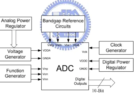
Expect for pipelined ADC, we propose a low power CMOS bandgap reference circuit. This bandgap reference circuit is designed by using MOSFETs operated in weak-inversion region instead of BJTs to reduce power consumption. Basically the bandgap reference circuit could provide stable reference voltages and bias voltages to our pipelined ADC. The relationship of bandgap reference circuit and pipelined ADC is shown in Figure 1.1.
Figure 1.1 The relationship of bandgap reference circuit and pipelined ADC
1.2 Thesis Organization
This thesis is organized into six chapters.
Chapter 2 describes the concepts of analog-to-digital conversion and performance parameters used to characterize ADCs. Then, several ADC architectures are introduced and the evolution of the pipelined ADC is presented. Then, the digital error correction technique and the 1.5-bit architecture are described. Finally, the timing of the pipelined ADC is analyzed.
Chapter 3 describes the key circuit blocks used in pipelined ADC. Among them are the operational amplifier, the common mode feedback, the comparator, the bootstrapped switch, the sample-and-hold amplifier (SHA), the 1.5-bit architecture, and the 2-bit flash converter. Then, the transistor level simulated results of each circuit are presented. Finally, the simulation of the whole pipelined ADC and its layout and floor plan are presented.
Chapter 4 presents the testing environment, including the component circuits on the DUT (device under test) board and the instruments. Then, the pipelined ADC described in Chapter 3 is fabricated in a standard TSMC 0.18µm CMOS Mixed-Signal process and the measured results of this chip are summarized.
Chapter 5 described the principle of the new low-power CMOS bandgap reference circuit. Finally, the simulated results of this CMOS bandgap reference circuit are presented with the standard TSMC 0.18µm CMOS Mixed-Signal process.
Chapter 2
General Design Consideration in
Pipelined A/D Converters
2.1 Introduction
Many practical integrated circuit realizations of pipelined A/D converters have been successfully implemented over past decade. This Chapter first presents the main performance parameters used to access the static and dynamic behaviors of Nyquist A/D converters and then introduces some of the prominent ADC architectures.
2.2 Performance Parameters In Nyquist A/D Converters
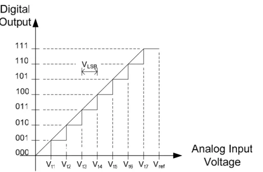
In conventional Nyquist A/D converter the accuracy can be defined by comparing every input sample and the corresponding output sample. Figure 2.1 illustrates the ideal conversion characteristic of a 3-bit ADC. The transition voltage can be written as , 2 ref tn N V V = ⋅n n∈
{
0,1, 2,..., 2N −1 ,}
(2.1)where N and Vref represent the bit numbers and the applied reference voltage
respectively. The quantization step (VLSB) is the difference of two transition voltages
and it can be written as
2
ref LSB N V
Figure 2.1 Ideal conversion characteristic of a 3-bit ADC
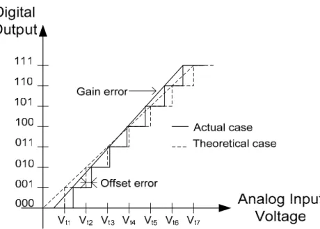
2.2.1 Offset and Gain Error
The error of an A/D converter is the difference between the theoretical and the actual input voltage required to produce a particular output code. In most applications the user can calibrate the offset and gain errors by subtracting the offset and dividing by the gain.
Offset error is the difference between the theoretical transition voltage and the actual transition voltage relatively to the quantization step. Gain error indicates the slope difference between the lines connecting the theoretical and actual transitions of the full scale extremes.
Figure 2.2 Illustrates Offset and Gain Error
2.2.2 Differential Non-Linearity Error (DNL)
DNL error is defined as the difference between an actual step width and the ideal
voltage of 1LSB (1
2
ref N V
LSB= ). For an ideal ADC, in which the differential
nonlinearity coincides with DNL = 0LSB, each analog step equals 1LSB and the transition voltages are spaced exactly 1LSB apart. A DNL error specification of less than or equal to 1LSB guarantees a monotonic transfer function with no missing codes. DNL is specified after the static gain error has been removed. It is defined as follows:
( )
( 1 ,) ( ), 1 1 t n actual t n actual V V DNL n LSB + − = − . (2.3)If the maximum DNL error is larger than -1 LSB at N-bit level, it is guaranteed that the ADC is monotonic, which means that the digital output always increases or is kept constant as the input increases. [01] [02]
2.2.3 Integral Non-Linearity Error (INL)
INL error is defined as the deviation of each transition voltage of each code from the ideal transition voltage. INL is the difference between the actual finite resolution characteristic and the ideal finite resolution characteristic. INL is also specified after the static gain error has been removed. It is defined as follows:
( )
( ), ( ) 1 t n actual t n ideal V V INL n LSB , − = . (2.4)Figure 2.3 displays examples of DNL and INL errors for different codes. [01] [02]
Figure 2.3 Example of DNL and INL errors in a 3-bit ADC
2.2.4 Signal-to-Noise Ratio (SNR)
the ADC’s output. It is well known that the theoretical SNR for an N-bit ADC is given by
6.02 1.76
SNR= ⋅ +N dB. (2.5)
2.2.5 Spurious Free Dynamic Range (SFDR)
The spurious free dynamic range is defined as the ratio of rms amplitude of the fundamental (the maximum signal amplitude) to the rms value of the largest distortion component in a specified frequency range. SFDR is important because noise and harmonics restrict converters’ dynamic range.
2.2.6 Signal-to-Noise and Distortion Ratio (SNDR)
For sinusoidal input signals, the signal to noise and distortion ratio is defined as the ratio of the signal power (maximum amplitude of the signal component) to the noise and harmonic distortion power at the ADC’s output.
2.2.7 Effective Number of Bits (ENOB)
For actual ADCs, a specification often used in place of the SNR or SNDR is ENOB, which is a global indication of ADC accuracy at a specific input frequency and sampling rate. ENOB can be defined as follows:
1.76 6.02
SNDR
2.3 Review of ADC Architectures
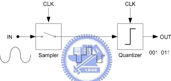
Analog-to-digital conversion can be separated into two distinct operations: sampling and quantization. Sampling transforms a continuous time signal into a corresponding discrete time signal. Quantization converts the continuous amplitude distribution into a set of discrete levels, which can be expressed with digital codes. Figure 2.4 illustrates the principle of A/D conversion.
Figure 2.4 Principle of A/D Conversion
Some A/D converter architectures, such as flash converter, can perform sampling and quantization simultaneously. In high performance ADCs, sampling and quantization are usually separated to make it possible to optimize the circuitry for both tasks without compromises. [02] [03]
2.3.1 Flash ADC
Flash ADC which is the fastest and one of the simplest ADC architecture is shown in Figure 2.5. It consists of 2N-1 comparators and performs 2N-1 level quantization.
The reference voltages of the comparators are generated by using a resistor ladder which is connected between the positive and the negative reference voltage: +Vref
and –Vref respectively. The set of 2N-1 comparator outputs is often referred to as
thermometer code and is converted to N-bit binary word with a logic circuit. The input signal of the flash ADC is directly connected to the inputs of the comparators thus the speed of the flash ADC is very fast and the speed is only limited by the speed of the comparators. Therefore the flash ADC is capable of high speed.
The drawback of the flash ADC is the fact that the number of the comparators grows exponentially with the number of bits. As the number of comparators increases the chip area and power consumption will also increase. Therefore the flash ADC is not suitable for high resolution application; typical resolutions are seven bits or below. Another drawback of the flash ADC is that the converter is sensitivity to comparator offset however the offset voltage can be solved by using auto-zeroing comparators.
2.3.2 Two-Step ADC (or Subranging ADC)
One way to reduce the number of comparators in flash ADC is to perform the quantization in two steps [04]. Therefore, the number of comparators can be reduced form 2N-1 to 2×2N/2. The block diagram of this two-step converter is shown in Figure 2.6. The operation of this converter is described as follows. The fine flash ADC determines the most significant bits then these bits are converted back to an analog signal through the DAC to be subtracted from the input signal. This residual signal is then sent to the coarse flash ADC to determine the least significant bits.
The two-step converter has a longer latency delay than the flash converter but it can allow for higher resolutions than the flash converter because of reducing the number of comparators.
Figure 2.6 Two-step ADC
2.3.3 Pipelined ADC
The block diagram of the pipelined ADC is shown in Figure 2.7. It consists of a cascade of M identical stages in which each stage produce k bits and the last pipelined stage is followed by a flash ADC providing p bits. As a result, the final resolution N is M×k+p.
Figure 2.7 m-bit/stage pipelined ADC
A function block diagram of one stage is shown in the inset of Figure 2.7. The incoming voltage is sampled by the S/H circuit and simultaneously digitized by the sub-ADC. The output signals of the sub-ADC are then converted back to analog forms and will be subtracted form the output signals of the S/H circuit. The resulting residue voltage is amplified by 2k. The S/H circuit, the D/A converter, the subtraction, and the amplification are all performed by a single circuit block which called multiplying analog-to-digital converter (MDAC). The MDAC circuit consists of an opamp and a set of switched capacitors. The sub-ADC is usually performed in fresh architecture and consists of a few comparators and logic gates.
When the input signal is a rapidly-changing signal, the relative timing of the first stage S/H circuit and the sub-ADC is critical but it can be relaxed with a front-end circuit. If the input signal is not a rapidly-changing signal a front-end S/H circuit is not needed, since the pipelined stage already contains an S/H circuit. [05]
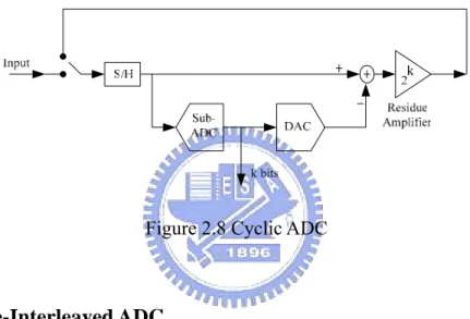
2.3.4 Cyclic ADC
A cyclic ADC consisted of a single pipeline stage with the output fed back to the input is shown in Figure 2.8. The operation of a cyclic ADC is the same as a pipelined ADC except that one stage does all the processing. The cyclic ADC completes N bits by reusing the stage multiple times thus it uses very little chip area and dissipates very low power. [06]
Figure 2.8 Cyclic ADC
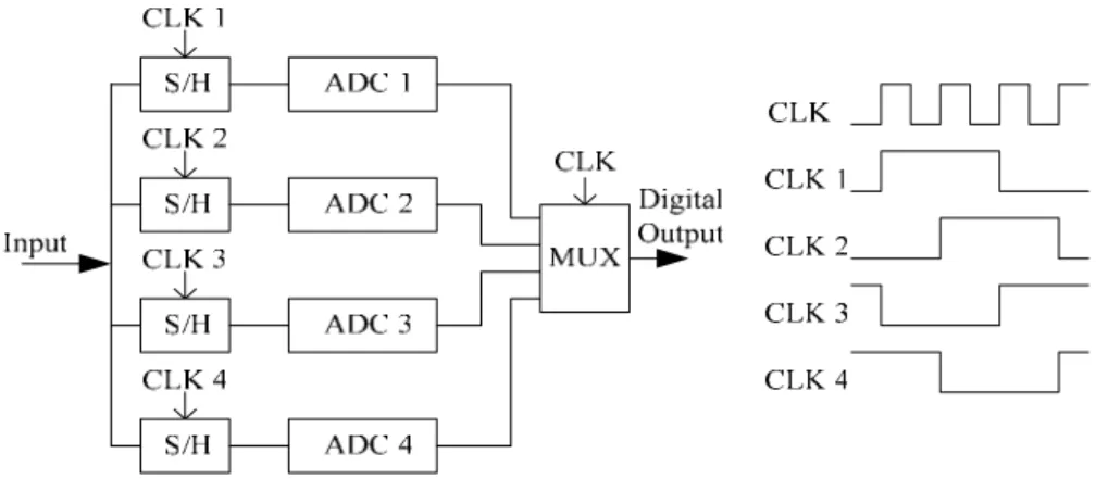
2.3.5 Time-Interleaved ADC
Figure 2.9 shows the block diagram of an architecture in which four ADCs are used on parallel to achieve four times the sampling rate of a single converter. This method is often known as time-interleaved architecture [07]. The sample-and-hold circuits consecutively sample and apply the input analog signal to their respective ADCs. The digital outputs of the channels are combined with a multiplexer to a single bit-stream. [02]
Figure 2.9 Four-channel time-interleaved ADC and its clock signals
2.4 Digital Error Correction Technique
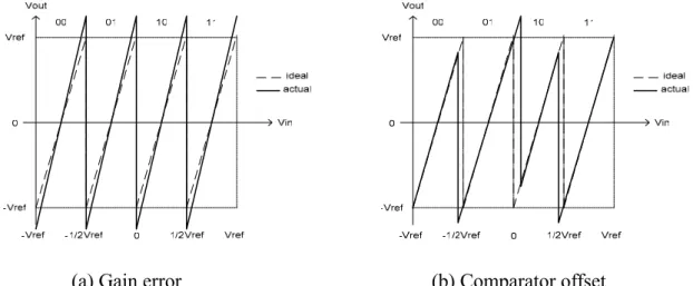
In the pipelined ADC, the input signal range is the same with the output signal range for each stage. This is done by the gain amplifier which amplifies the residue subtracted from the input signal. The amplified residue must still within the conversion range for the next stage. If there is a deviation such as the amplified residue exceeds the conversion range of the next stage, it may have wrong codes. As illustrated in Figure 2.10, the gain error and comparator offset may lead to over conversion range problems. Digital error correction is the name of the calibration technique that reduces the gain error, keeps the conversion range constant with modified coding and tolerates greater comparator offset.
For example, in a 2-bit pipelined stage there is only a contribution of less than two bits to final output word of the A/D converter and the residue amplification gain used is usually smaller than 4. This will keep the residue within certain boundaries and therefore the extra redundancy can be used to correct in the digital domain the referred non-ideal effects in the Flash Quantizers. Figure 2.11 shows the modified coding transfer curve with digital error correction.
(a) Gain error (b) Comparator offset Figure 2.10 Residue amplification characteristic of a 2-bit/stage with
(a) Gain error (b) Comparator offset
Figure 2.11 Analog residue with digital error correction
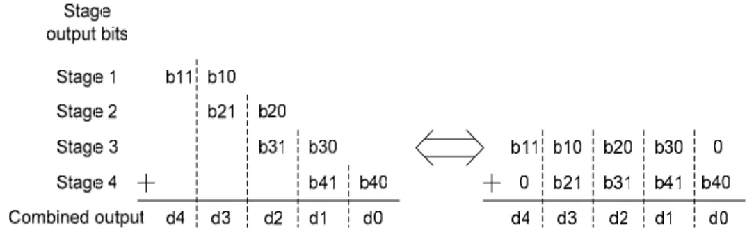
In the digital domain the correction is a simple addition, as illustrated in Figure 2.12. On the left is shown how the bits of the final result are obtained by summing the output bits of the stages with one-bit overlap. On the right the same bits are rearranged to show how the correction can be performed with a single adder. [05] [08]
Figure 2.12 RSD correction in digital domain
2.5 1.5-Bit / Stage Architecture
The pipelined ADC uses a pipelined 1.5-bit/stage architecture with 9 stages as shown in Figure 2.13. Each stage resolves 2 bits with a sub-ADC, and subtracts this value form its input and amplifies the resulting residue by a gain of two. The input signal range of the pipelined ADC is from –Vref to +Vref. In the 1.5-bit/stage, we set the threshold voltages of the sub-ADC at –Vref/4 and +Vref/4, therefore the residue transfer function is given as follows
( )
( )
( )
2 2 2 2 , 0 4 2 , 01 4 4 2 , 1 4 ref in ref ref in ref ref out in in ref in ref in ref V V V if V V D V V V V if V D V V V if V V D − ⎧ + − < < ⇔ = ⎪ ⎪ − + ⎪ =⎨ < < ⇔ ⎪ + ⎪ − < < + ⇔ = ⎪ ⎩ 0 0 = (2.7)where D is the binary output code for each stage. The transfer function of 1.5-bit/stage is shown in Figure 2.11. Because of using the digital error correction technology, the 1.5-bit/stage has lower (2 instead of 4) inter-stage gain than the 2-bit/stage, but it requires more stages (9 stages instead of 5 stages for 10bits ADC) than the 2-bit/stage. By reducing the inter-stage gain, the accuracy requirements on the sub-ADCs are
greatly reduced. In this research, a maximum offset voltage of Vref/4 can be tolerated before the bit errors occur.
Figure 2.13 Pipelined ADC with 1.5-bit/stage architecture
The number of bits per stage has a serious impact on the power, speed, and accuracy requirements of each stage. Therefore, the best choice of bit/stage is decided on the overall ADC specifications. For example, for fewer numbers of bits per stage, the comparator requirement is more relaxed, and the inherent speed of each stage is faster. The higher speed gain is because the inter-stage gain is lower allowing higher speed due to the fundamental gain bandwidth tradeoff of amplifiers. If fewer bits per stage are used, more stages are required. Therefore, the noise and gain errors of the later stages would make more inaccuracy to the overall converter because of the low inter-stage gain. Thus, low speed, high resolution specifications tend to favor higher number of bits per stage, where high speed, low resolution specifications favor a lower number of bits per stage.
This 1.5-bit/stage architecture has been shown to be effective in achieving high throughput at low power consumption. The low number of bits per stage combined with digital error correction technology relaxes the limits on the comparator offset voltage and DC gain of op-amp. [08]
2.6 Timing Analysis of The Pipelined ADC
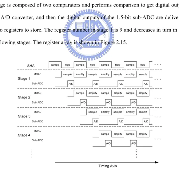
The operation of the pipelined ADC is best understood with a timing diagram. Figure 2.14 illustrates the timing of the pipelined ADC. The 1.5-bit sub-ADC in each stage is composed of two comparators and performs comparison to get digital output of A/D converter, and then the digital outputs of the 1.5-bit sub-ADC are delivered into registers to store. The register number in stage 1 is 9 and decreases in turn in the following stages. The register array is shown in Figure 2.15.
Stage 1 Stage 2 Stage 3 Stage 4 Stage 5 Stage 6 Stage 7 Stage 8 Stage 9
Register Register Register Register Register Register Register Register Register Register Register Register Register Register Register Register Register Register Register Register Register Register Register Register Register Register Register Register Register Register Register Register Register Register Register Register Register Register Register Register Register Register Register Register Register Register Register Register Register Register Register Register Register Register Register D0 D1 D2 D3 D5 D6 D7 D8 D4 D9 D igital Err o r C o rr ecti on T e c hnology Ø1 Ø2
Figure 2.15 Register array of the pipelined ADC
In Figure 2.15, ø1 and ø2 are two non-overlapping signals, and by passing register array, digital outputs from 9 stages can enter digital error correction block concurrently. The ten registers after digital error correction block make 10 digital outputs come out at the same time.
Chapter 3
Design of Pipelined Analog-to-Digital
Converter
3.1 Introduction
Traditional designs of high-speed CMOS analog-to-digital converters have used flash architectures. While flash architectures usually yield the highest throughput rate, they trend to require large silicon area because of the large numbers of comparators required. An important purpose is that the realization of high-speed ADC in smaller area than that required in flash converters so that the A/D interface function can be integrated on the same chip with associated image-processing functions. Multistage conversion architectures reduce the area by reducing the number of comparators. Using a pipelined architecture allows the stages to operate concurrently and produces the maximum throughput rate. Also, digital error correction technology significantly reduces the sensitivity of the architecture to certain component non-idealities.
The pipelined ADC architecture has been adopted into many high-speed applications such as high-performance digital communication systems and high-quality video systems. The rapid growth in these applications is driven the design of ADCs toward higher sampling rate, lower power consumption, and smaller chip area. The continued scaling of submicron CMOS technology couples with lower power supply voltage. This trend gives a challenge to conventional pipelined ADC designs which rely on high-gain and large-bandwidth operational amplifiers (op-amp)
to produce high-accuracy and high-speed data converters. At low power supply voltage, large open-loop operational amplifier gain is difficult to realize without sacrificing bandwidth or power consumption. As a result, the finite operational amplifier gain is becoming a major problem in achieving both high speed and high accuracy. One way to get a high op-amp gain is usually realized by multistage op-amp structure, gain-boosting technique, and long channel devices.
3.2 Operational Amplifier
Speed and accuracy are two of the most important properties of analog circuits, however optimizing circuits for both aspects lead to contradictory demands. In a wide variety of CMOS analog circuits such as switched-capacitor (SC) circuits, sample-and-hold amplifiers, and pipelined ADC, speed and accuracy are determined by the settling behavior of operational amplifiers. Fast settling requires a high unity-gain frequency, whereas accurate settling requires a high dc gain.
The realization of a CMOS operational amplifier that combines high dc gain with high unity-gain frequency has been a difficult problem. The high-gain requirement leads to multistage designs with long-channel devices, whereas the high unity-gain frequency requirement needs a single-stage design with short-channel devices. One way to overcome this problem is using the cascoding technique. Cascoding technique can enhance the dc gain of an op-amp without degrading the high frequency performance. The dc gain of the op-amp is proportional to the square of the intrinsic MOS transistor gain gm×ro.
architecture. The advantages of the fully-differential circuit are that it can reduce even-order harmonic distortion, substrate noise, and common-mode disturbances. It also improves the power supply rejection ratio (PSRR) and the common-mode rejection ratio (CMRR). One drawback in the fully-differential circuit is that it needs the common-mode feedback circuit and it will be illustrated in the following sections.
3.2.1 Folded Cascode Operational Amplifier
The op-amp is the most important element in every stage of the pipelined ADC. If we increase the frequency bandwidth of the op-amp, the converting speed of the pipelined ADC can be increased. However, if we increase the dc gain of the op-amp, the resolutions of the pipelined ADC can be increased. In this project, the operational amplifier is made in folded cascode architecture. The folded cascode op-amp is shown in Figure 3.1. However, the dc gain of the folded cascode op-amp is limited by the short-channel devices and the effective gate-driving voltage. For this reason, it is necessary to use the op-amp open-loop gain enhancement technique to increase the dc gain of the op-amp. This method is called gain-boosting, and the theory will be illustrated as follows.
The dc gain of the fully-differential folded cascode op-amp of Figure 3.1 can be written as
v m out
A =G ×R . (3.1)
The output impedance Rout is expressed as Rout =Rop||Ron. Where Rop can be
written to Rop ≈
(
gm9 +gmb9)
r ro11 o9 , and Ron can be written to(
7 7) (
7 2||on m mb o o o5
)
R ≈ g +g r r r . Thus the output impedance Rout is shown as
Rout =⎡⎣
(
gm9+gmb9)
r ro11 9o ⎦ ⎣⎤ ⎡||(
gm7+gmb7) (
ro7 ro2||ro5)
⎤⎦. (3.2)The transconductance is approximately equal to . Substituting equation (3.2)
into equation (3.1), we obtain
m G gm2
(
)
(
) (
{
)
}
2 9 9 11 9 || 7 7 7 2|| 5 v m m mb o o m mb o o o A =g ⎡⎣ g +g r r ⎦ ⎣⎤ ⎡ g +g r r r ⎤⎦ . (3.3)Op-amps used in feedback circuits indicate a large signal behavior called “slewing”. The slewing behavior of the folded cascode op-amp is shown in Figure 3.2. Figure 3.2(a) and (b) illustrate the equivalent circuit for positive and negative step
inputs respectively. The NMOS current sources supply currents of In, however the
current that discharges or charges the load capacitor CL is equal to ISS. So the slew rate
of the folded cascode op-amp can be expressed as ±ISS/CL. Note that the slew rate is
independent of In if In>ISS.
In Figure 3.2(b), if ISS>In and the op-amp is slewing, M7 turns off such that M1
and the tail current source will enter the liner region. After M2 turns on, the circuit
returns to the equilibrium state, at the same time the drain voltage of M5 will
experience a large swing and this phenomenon will slow down the settling behavior. [10]
(a)
(b)
Figure 3.2 Slewing behavior of the folded cascode op-amp
3.2.2 Gain-Boosting Technique
A very widely-used technique to enhance the op-amp dc gain without going into multistage architectures is based on improving the cascoding effect of a single MOS transistor by using local negative feedback [11]. The resultant circuit, often referred to as regulated cascode, is shown in Figure 3.3. The auxiliary amplifier encloses the
cascode transistor M2 in a feedback loop, making the voltage on its source node
almost constant. As a result, the output impedance is given by
1 2 2
out m o o1
R ≈ A g r r . (3.4)
Thus the regulation improves the impedance by the gain of the auxiliary amplifier A1
and the dc gain of the op-amp is increased by the same amount. [10]
Figure 3.3 Increasing the output impedance by feedback
Shown in Figure 3.4 is a folded cascode op-amp with gain-boosting technique used in this project, the output impedance of such a boosts of the PMOS current sources as well, thereby getting a very high gain.
3.2.3 The Common-Mode Feedback (CMFB) of Switched Capacitor
In the previous section, we have discussed the advantages about the fully-differential op-amp. As we know, fully-differential circuits provide better rejection of common-mode (CM) noise and high-frequency power-supply variations compared to their single-ended circuits. However, since the CM loop gain from the external feedback loop around the fully-differential op-amp is small, the CM voltage in fully-differential circuits is not precisely defined. Without proper control, the output CM voltage tends to drift to the supply rails due to power-supply variations, process variations, offsets, etc. Hence, an additional CM feedback loop is usually necessary. The circuit comprising this CM feedback loop is called the CM feedback (CMFB) circuit.
The CMFB circuit performed in switched-capacitor (SC) is shown in Figure 3.5. The main advantages of SC-CMFB are that they impose no limits on the maximum allowable differential input signals, have no additional parasitic poles in the CM loop, and are highly linear. However, SC-CMFB injects nonlinear clock-feedthrough noise into the op-amp output nodes and increases the load capacitance that needs to be driven by the op-amp. Hence, SC-CMFB is typically only used in switched-capacitor applications such as sample-and-hold amplifier and SC-filter.
During clock phase ø1, C1p and C1n are connected to C2p and C2n, respectively. The
dc voltage across C2p and C2n is determined by C1p and C1n, respectively, and is
refreshed every ø1 clock phase. During clock phase ø2, C1p and C1n are charged to
VCM-Vb and capacitors C2p and C2n generate the control voltage Vcmfb and the output
voltage of Voutp and Voutn. [12]
3.2.4 Simulation Result of The Folded-Cascode Op-Amp
Figure 3.6 shows the AC simulation results including the gain and phase margin of five process corners (TT, FF, FS, SF, SS). The simulated slew rate response of the op-amp is shown in Figure 3.7. The simulated performance of the fully-differential folded cascode op-amp is summarized in Table 3.1.
TT process corner ◦DC gain︰82.7dB ◦Phase margin︰66.2° ◦Unity gain freq.︰530.5MHz
@2pF load capacitor
Figure 3.7 Simulated slew rate result of the op-amp
Table 3.1 Summary of the simulation results of the op-amp Folded-Cascode Op-amp
DC Gain 82.7dB
Phase Margin 66.2°
Unity Gain Bandwidth 530.5MHz
Load Capacitor 2pF
Common Mode Input Range 0.3V~1.4V
Output Swing 0.35V~1.45V Rise 202V/µs Slew Rate Fall 311V/µs Settling Time 4.56ns Power Dissipation 5.34mW Process TSMC 0.18µm 1P6M Process
3.3 Comparator
A fully-differential CMOS dynamic comparator topology suitable for pipelined ADC with a low stage resolution is used in this project and shown in Figure 3.8. The comparator, based on two cross coupled differential pairs and switchable current sources, has a small power and area dissipation and it is shown to be very insensitive to transistor mismatch. In order to make the comparator insensitive to mismatch and process variations, all transistors should be operated in saturation region after the latching signal applied.
Figure 3.8 Schematic diagram of comparator circuit
The operation of the comparator is described as followed. Where transistors M1~M4 are the two cross coupled differential pairs, M5 and M6 are the current source
transistors, and M7~M12 forms the latches. When the comparator is inactive the latch
signal Vlatch is at 0V, which means that the current source transistors M5 and M6 are
the switch transistors M9 and M12 reset the outputs by shorting them to Vdd. The
transistors M7 and M8 of the latch conduct and force the drains of all the input
transistors M1~M4 to Vdd. When the Vlatch is risen to Vdd the outputs are disconnected
from the positive supply and the switching current sources M5 and M6 enter saturation
regions and begin to conduct. These two transistors determine the bias currents of the two differential pairs M1 - M2 and M3 - M4, respectively. Therefore, the threshold
voltage of the comparator is determined by the current division in the differential pairs and between the cross coupled branches. [13] [14]
Figure 3.9 shows the simulation result of the output signal when applying the sine-wave input into the comparator.
Figure 3.9 Simulated result of the comparator
3.4 Bootstrapped Switches
Figure 3.10 shows the well known gate-source bootstrapping technique. It shows the signal switch MNSW together with five additional switches (S1~S5) and an additional capacitor C. Switches S3 and S4 charge the capacitor during ø2 to VDD.
During ø1, switches S1 and S2 connect the pre-charged capacitor in series with the
input voltage Vin such that the gate-source voltage of transistor MNSW is equal to the
voltage VC ( ≅ VDD) across the capacitor. This guarantees maximum switch
conductance independent of Vin. This advantage is that the constant RON due to the
fixed VGS makes the time constant τ=RON×C independent of the input signal. This will
decrease the harmonic distortion. The fixed VGS also eliminates the high gate oxide
voltage when the input signal is low. Switch S5 fixes the gate voltage of MNSW to VSS during ø2 to make sure that the transistor is in the OFF state.
Vout Vin MNSW VDD VSS VSS C ø1 ø1 ø2 ø2 ø2 S3 S4 S1 S2 S5 VGS VC
Figure 3.10 Basic circuit of the bootstrapped switch
Figure 3.11 shows the transistor-level implementation of the bootstrapped-switch circuit shown in Figure 3.10. Transistors MN1, MP2, MN3, MP4, and MN5 correspond to the five ideal switches S1~S5 respectively. The transistor MN6S triggers MP2 on at the beginning of ø1 while transistor MN6 keeps it on as the voltage
on node D rising to the input voltage Vin. Gate connections of transistors MN1 and
MN6 allow them to be turned on similar to the main switch MNSW. Furthermore, transistor MNT5 has been added to prevent the gate–drain voltage of MN5 from exceeding VDD during ø1 while it is off. During ø1 when MNT5 is off, its drain-bulk
diode junction voltage reaches a reverse bias voltage of 2VDD. This must be
compatible with the technology limits. It should be also noted that the bulk of transistors MP2 and MP4 must be tied to the highest potential, i.e., node B, and not to VDD.
However, the voltage at the drain side of the main switch MNSW must be always higher than that at the source side at the switching moment to prevent the drain–gate voltage from exceeding VDD during the turn-on transient. In spite of the fact that the
gate–source potential of the bootstrapped switch is held constant, the conductance drops with the source voltage due to the source-bulk potential which increases the threshold voltage. [16] [17]
3.5 Sample and Hold Amplifier
The front-end sample-and-hold amplifier (SHA) is shown in Figure 3.12. Figure 3.13 shows the non-overlapping clock phases used in this project. During the sampling phase (phase ø1), capacitors CS are connected to the differential inputs Vin
outputs of the op-amp are connected together in a negative feedback configuration. This makes the differential voltages at these nodes to be equal to the input offset voltage of the op-amp, Voffset. Therefore, the capacitors CS are charged to Vin-Voffset.
During the holding phase (phase ø2), the capacitors CS are connected between the
inputs and the outputs of the op-amp. This will make the differential output voltages to be equal to Vin without regard to the input offset voltage of the op-amp. It means
that the SHA reduces the offset error of the op-amp by storing the error during one clock phase and subtracting this error from the signal during the next phase. At the end of the holding phase, the differential output voltage is given by
1 1 offset in out V V A V A + = + , (3.5) where A is the dc gain of the op-amp. For very large A, the equation 3.5 can be approximated as
out in
V ≅V . (3.6)
Since the sampling and the holding capacitors use the same capacitors, this SHA has no gain-error due to the capacitor mismatch. However, the SHA is not suitable for processing single-ended signals because this circuit lack the inherent single-ended to fully-differential conversion capability. However, the single-ended signals will not be used in this project.
Since this SHA is supposed to be used in the front-end of the pipelined ADC, the size of the capacitors should be chosen in order to reduce the sampled thermal noise (kT/C) to an acceptable level. [15]
Figure 3.12 Schematic diagram of sample-and-hold amplifier circuit
Figure 3.13 Non-overlapping clock phases
Figure 3.14 shows the simulation result of the SHA when applying the sine-wave input of 0.25MHz (frequency) with the amplitude of ±600mV. Figure 3.14(b) is the zoom-in result of Figure 3.14(a).
(b)
Figure 3.14 Simulated result of the SHA sampling the input sine-wave
3.6 The 1.5-Bit Sub-ADC (Flash Quantizer)
As previously mentioned in section 2.5, in a pipelined ADC, the function of the sub-ADC is to convert the held input of the previous stage into low resolution digital codes. Traditional N-bit flash converters employ a resistor-string for the division of the reference voltage for defining the decision levels combined with 2N-1 comparators. In this project, the 1.5-bit sub-ADC uses only 2 comparators in its implementation.
For a 1.5-bit sub-ADC, a comparator offset voltage up to ±Vref/4 can be tolerated through digital error correction technology. The comparator structure employed in the 1.5-bit sub-ADC is shown in Figure 3.8, and the 1.5-bit sub-ADC is shown in Figure 3.15. Where the MSB and LSB are the digital output codes of the 1.5-bit sub-ADC, and the X, Y, and Z are the controlled signals which will be applied to the MDAC. Table 3.2 summaries the digital output codes of MSB and LSB and the controlled signals of X, Y, and Z for different values of the differential input voltage. Figure 3.16 shows the simulated result of the 1.5-bit sub-ADC, where the ±Vref are set equal to ±600mV.
Figure 3.15 Schematic of the 1.5-bit Sub-ADC
Table 3.2 Digital output codes and controlled signals of 1.5-bit sub-ADC Differential Input Voltage
(Vin)
Digital Output Codes (MSB, LSB) Controlled Signals (X, Y, Z) 4 ref ref in V V V − − < < 00 010 4 4 ref ref in V V V − + < < 01 001 4 ref in ref V V V + < < + 10 100
3.7 The 1.5-Bit MDAC
Figure 3.17 shows the schematic of the 1.5-bit MDAC circuit, which consists of an op-amp, four equal sized capacitors and 13 switches. In a pipeline stage the function of the MDAC is twofold. First, it provides the sample-and-hold operation required for the pipelining, second, it performs the analogue reconstruction of the digital code resulting from the sub-ADC, subtracts it from the analogue sampled voltage, Vin, and multiplies the resulting residue by 2. Phase ø1 and phase ø2 are two
non-overlapping signals and phase ø1_d is a delayed version of phase ø1 but still
non-overlapping with phase ø2. During phase ø1 (sampling phase), the two pairs of
capacitors Cs and Cf sample the differential input Vinp and Vinn. Next, during phase
ø2 (residue amplification phase), the integrating capacitors, Cf, form the feedback
loop of the op-amp while the bottom plates of the sampling capacitors are connected to each other, to the positive reference (Vrefp), or to the negative reference (Vrefn) depending on the state of controlled signals X, Y, and Z. Assuming Cs=Cf=C and the a non-ideal op-amp with finite DC gain, A, and offset voltage Voffset, at the end of
phase ø2, the value of the amplified residue to be processed by the next stage of the
pipeline is given approximately by 2 2 , 1 2 4 1 2 2 , 1 2 4 4 1 2 2 , 1 2 4 1 offset in ref ref ref in offset in ref ref out in offset in ref ref in ref V V V V A if V V Y A V V V V A V if V A V V V V A if V V X A ⎧ + + ⎪ − Z − < < ⇔ = ⎪ ⎪ + ⎪ ⎪ ⎪ + − + ⎪ =⎨ < < ⇔ = ⎪ + ⎪ ⎪ ⎪ − + + ⎪ < < + ⇔ = ⎪ + ⎪⎩ , (3.7)
yielding for very large A
2
out in ref ref
V ≅ ⋅V − ⋅X V + ⋅Y V , (3.8)
where X, Y, and Z are the encoded digital outputs provided by the 1.5-bit sub-ADC.
Figure 3.17 Schematic of the 1.5-bit MDAC
Figure 3.18 shows the simulation output waveform of the MDAC circuits. The input signal Vin is first applied to front-end SHA, then the output signal of the SHA is applied to the 1.5-bit MDAC and the 1.5-bit sub-ADC.
3.8 The 2-Bit Flash ADC
The final stage of 2-bit flash ADC is shown Figure 3.19. A typical architecture of a 2-bit flash quantizer requires a bank of 3 comparators to achieve 2 bits of resolution. Figure 3.20 shows the simulation result of the 2-bit flash ADC
Figure 3.19 Schematic of the 2-bit Flash ADC
3.9 Simulated Results of Pipelined ADC
The architecture of the 10-bit, 80MS/s pipelined A/D converter with the 1.8V supply voltage shown in Figure 3.21 had simulated with eight identical 1.5-bit stages and one 2-bit flash converter. In the simulation, we use the ideal DAC to convert digital outputs of the pipelined ADC to analog signal. Figure 3.22 shows the simulated result of the pipelined ADC when applying the 1 MHz sine-wave to the inputs.
Figure 3.22 Simulated result of the pipelined ADC with the sine-wave input signal
Figure 3.23 shows the simulated results through the ideal DAC when applying the ramp signal to input. Then the results are analyzed for characterizing the linearity of the ADC. However, the linearity of the ADC could be realized by analyzing the parameters of the DNL and INL. The simulated results of the DNL and INL of the pipelined ADC are shown in Figure 3.24. The maximum DNL and INL are ±0.7 LSB and ±1.0 LSB respectively.
(a) DNL (b) INL Figure 3.24 Simulated results of DNL and INL
Table 3.3 summaries the simulated results of the pipelined ADC. Layout and floor plan of the experimental prototype chip are shown in Figure 3.25. This pipelined ADC
was laid out on a 1.388×1.392 mm2 die that including digital circuits and the pad
frame. In the layout, we use the mirror symmetry to enhance the rejection of common mode noises in the fully differential circuits. In this research, the analog circuit is separated from the digital circuit and is powered from a separated power supply.
Table 3.3 Summary of simulated results of the pipelined ADC
Parameters Simulated Results
Process TSMC 0.18µm CMOS
Mixed-Signal
Supply Voltage 1.8 V
Input Range ±0.6V Fully differential
Resolution 10 bits Operation Frequency 80 MHz DNL ±0.7 LSB INL ±1.0 LSB SFDR (Fin=1MHz) 58 dB Power Dissipation 85 mW Chip Size 1.388mm×1.392mm (a) Layout
(b) Floor plan
Chapter 4
Test Setup and Experimental Results
4.1 Introduction
This pipelined ADC has been designed and laid out by using the TSMC 0.18µm CMOS Mixed-Signal process with one poly and six mental. In this chapter, we present the testing environment, including the component circuits on the DUT (device under test) board and the instruments. The measured results are presented in this chapter, too.
4.2 Test Circuits
Figure 4.1 Testing setup
Figure 4.1 shows the testing setup used to measure the performance of the experimental pipelined ADC described in this project. It contains analog power
regulator, digital power regulator, clock generator, function generator, logic analyzer, and etc. The supply voltages for analog and digital power regulators are supplied by the 9V batteries. In order to present the digital noise coupling to the analog circuits, the analog ground and digital ground are isolated to each other.
The input signal to the DUT is provided by the signal generator, Agilent E4438C. The photograph of the signal generator is shown in Figure 4.2. The output bit streams of the DUT are sent to the logic analyzer, HP 16702B which is shown in Figure 4.3. The clock signal of the system is generated with a signal generator, HP 8648C, where its output signal is fed to the pulse generator, HP 8133A, to generate the clock signal. The photograph of the clock generators are shown in Figure 4.4.
Figure 4.2 Signal Generator Agilent E4438C
Figure 4.4 Clock generator, the top instrument is signal generator HP 8648C, and the bottom instrument is pulse generator HP 8133A
4.2.1 Power Supply Regulators
The analog and digital power supplies are generated by the application of the LM317 adjustable regulators shown in Figure 4.5. The diodes D1 and D2 are the protection diodes. The capacitor C1 is used to improve the ripple rejection and capacitor C2 is the input bypass capacitor. The resistor R1 is the fixed resistor and resistor R2 is the precise variable resistor. The output voltage of the Figure 4.2 can be expressed as 2 1.25 1 2 1 out ADJ R V R ⎛ ⎞ = ⋅ +⎜ ⎟⋅ ⋅ ⎝ ⎠ I R , (4.1)
where IADJ is the DC current that flows out of the adjustment terminal ADJ of the
regulator. By the way, the resistor R1 can use the low temperature coefficient of the metal film resistor to get the stable output voltage. [23]
Figure 4.5 Power supply regulator
The outputs of the regulators are bypassed on the PCB with the filter tank. The bypassed filter network is combined by 10uF, 1uF, 0.1uF, and 0.01uF capacitors as shown in Figure 4.6. The capacitor arrangement in Figure 4.6 provides decoupling of both low frequency noise with large amplitude and high frequency noise with small amplitude. [24] [25]
Figure 4.6 Bypass filter at the output of the regulator
4.2.2 Reference and Bias Voltage Generators
Figure 4.7 shows the schematic of the reference and bias voltage generators. The function of this circuit is to generate the low noise dc voltage source implemented with OP27 operational amplifier. The operational amplifier acts as a unity gain buffer for the voltage set by the potentiometer R1 at its input. The terminal Vdd_in is connected from the LM317 voltage regulator described in section 4.2.1. The voltage
of both +9V and -9V are supplied by the power supply instrument. [24]
Figure 4.7 Reference and bias voltage generator
4.3 The Package and Pin Configuration
Figure 4.8 shows the die photomicrograph of the experimental pipelined ADC and Figure 4.9 shows the photograph of the testing DUT board. Figure 4.10 presents the pin configuration and lists the pin assignments of the experimental pipelined ADC.
Pin Name I/O Describe 1 NC - No connection 2 NC - No connection 3 NC - No connection 4 NC - No connection 5 NC - No connection 6 NC - No connection 7 CLOCK In System clock input 8 DGND In Digital ground 9 DVDD In Digital power supply 10 AGND In Analog ground 11 NC - No connection 12 AVDD In Analog power supply 13 REFP In Reference voltage>Vcm 14 REFN In Reference voltage<Vcm 15 NC - No connection 16 D0 Out Digital data output 17 D1 Out Digital data output 18 D2 Out Digital data output 19 D3 Out Digital data output 20 D4 Out Digital data output 21 D5 Out Digital data output 22 D6 Out Digital data output 23 D7 Out Digital data output 24 D8 Out Digital data output 25 D9 Out Digital data output 26 NC - No connection 27 AGND In Analog ground 28 Vbb4 In Bias voltage 29 Vbb1 In Bias voltage 30 Vba4 In Bias voltage 31 Vba1 In Bias voltage 32 Vcm In Common mode voltage 33 Vinp In Input signal (0°) 34 Vinn In Input signal (180°) 35 AVDD In Analog power supply 36 NC - No connection 37 NC - No connection 38 NC - No connection 39 NC - No connection 40 NC - No connection NC
Top View
2 1 4 3 6 5 8 7 10 9 12 11 14 13 16 15 18 17 20 19 40 39 38 37 36 35 34 33 32 31 30 29 28 27 26 25 24 23 22 21 NC NC NC NC NC CLOCK DGND DVDD AGND AVDD NC REFP REFN NC D0 D1 D2 D3 D4 D8 D7 D6 D5 Vcm Vba1 Vba4 Vbb1 Vbb4 AGND NC D9 NC NC NC NC NC AVDD Vinn Vinp4.4 Experiment Results of Pipelined ADC
The pipelined ADC has fabricated in 0.18µm CMOS process. The chip was powered by the 1.8 V analog and digital circuits supply. A 1 MHz sine wave is applied to the ADC and operates at the 65 Msample/s conversion rate. The output 10-bit streams of the DUT collected by the logic analyzer and the plot chart are shown in Figure 4.11.
(a) Output bit streams
(b) Plot chart
From the measured results shown in Figure 4.11, the signal to noise ratio is calculated by collecting 16384 samples of the input signal and performing a 16384 point fast Fourier transform shown in Figure 4.12. This result shows that SNR is about 37.2 dB, and the SNDR is about 31.8 dB due to severe harmonic distortions. The SFDR shown in Figure 4.12 is about 38.1 dB.
Figure 4.12 16384 points FFT at 1MHz input frequency and 65 MHz sampling frequency
These harmonic distortions are caused by the nonlinear of the op-amp and mismatch of the output pairs. The worst reason is that the DC gain of the op-amp at the highest output swing is no longer large enough to meet the required specification. Furthermore, the charge injection and common mode drift issues both are the possible reasons. In addition, when the sampling rate is large than 65 Msample/s, the plot chart of the ADC doesn’t show the similar sine-wave. Probably the input signal and the sampling rate are coupled each other, thus the input signal is influenced and doesn’t like sine-wave anymore. Figure 4.13 shows the SNDR for different sampling rate. Table 4.1 summaries the measured results of the pipelined ADC.
0 5 10 15 20 25 30 35 40 45 40 50 60 65 sampling rate (MHz) SN D R ( dB ) fin=1 MHz fin=2 MHz
Figure 4.13 The SNDR against the sampling rate
Table 4.1 Summary of measured results of the pipelined ADC
Parameters Measured Results
Process TSMC 0.18µm CMOS
Mixed-Signal
Supply Voltage 1.8 V
Input Range ±0.6V Fully differential
Operation Frequency 65 MHz SNR for a 1 MHz input 37.2 dB SNDR for a 1 MHz input 31.8 dB SFDR for a 1 MHz input 38.1 dB ENOB 5 bits Power Dissipation 79 mW Chip Size 1.388mm×1.392mm
Chapter 5
Design of Low-Power CMOS Bandgap
Reference Circuit
5.1 Introduction
In most analog integrated circuits, bandgap reference voltage generators become the indispensable circuits in operation amplifiers, digital-to-analog converters, and analog-to-digital converters. The reason bandgap reference circuit becomes so important is that it can generate the stable reference voltage which is insensitive to the variation of the temperature and the supply voltage. With the growth of wireless communication systems and portable devices, low-power consumption and low supply voltage operation have become a popular research.
Recently, research on generating a low-power and low supply voltage reference circuit was based on discussing the properties of MOSFETs operated in the weak inversion. In the traditional bandgap reference, the BJTs can be replaced by the MOSFETs which operated in the weak inversion and these MOSFETs can generate the current which has direct proportion to temperature. With the MOSFETs operated in the weak inversion, the reference circuit consumes less current and further reduces the power consumption. The proposed bandgap reference circuit will be illustrated in the next section.
5.2 Bandgap Reference Circuit Configuration
The proposed bandgap reference circuit is shown in Figure 5.1. The elements M1 and M2 connect in a current mirror and serve for realizing the function of self-biasing. The MOSFETs M3 and M4 are designed to operate in the weak inversion such that the low-power reference circuit can be achieved. The current mirror of M1 and M2 is designed to make the drain currents of M3 and M4 operate in the weak inversion, then the voltage across R1 is proportional to the absolute temperature (PTAT). Hence, the resistor ratio R2/R1 can be used to compensate for the variation of the gate-source voltage of M4 with respect to the temperature. The detail circuit analysis will be illustrated in the next section. [18] [19] [20]
![Figure 2.3 displays examples of DNL and INL errors for different codes. [01] [02]](https://thumb-ap.123doks.com/thumbv2/9libinfo/7491329.115162/20.892.205.717.540.905/figure-displays-examples-dnl-inl-errors-different-codes.webp)