Low Temperature Radio-Frequency-Sputtered
„Ba, Sr…TiO
3Films on Pt
ÕTiNÕTiÕSi Substrates with Various
Oxygen
ÕArgon Mixing Ratios
Der-Chi Shye,aBi-Shiou Chiou,a,zMing-Jiunn Lai,aChuan-Chou Hwang,a Cheng-Chung Jiang,bJyh-Shin Chen,bMing-Hwu Cheng,b
and Huang-Chung Chengb,
*
aDepartment of Electronics Engineering and Institute of Electronics, National Chiao Tung University, Hsinchu 30010, Taiwan
b
Precision Instrument Development Center, National Science Council, Hsingchu Science-Based Industrial Park, Hsinchu 300, Taiwan
(Ba,Sr)TiO3共BST兲 films were fabricated on Pt/TiN/Ti/Si substrates by low temperature radio frequency magnetron cosputtering at 300°C. Material and electrical properties of BST films sputtered at low temperatures are significantly affected by the O2/(Ar ⫹ O2) mixing ratio共OMR兲. Plasma emission spectra indicate that the deposition rate declines at a higher OMR due to oxide formation on the target surface. The dielectric constant of the BST films can reach a maximum of 364 at 5% OMR. The ten-year lifetime of the time-dependent dielectric breakdown implies that the reliability of the capacitor can be enhanced at a higher OMR due to compensation of oxygen vacancies and smaller grain sizes. Current-voltage analysis indicates that the leakage current of the Pt/BST/Pt capacitor is limited by Schottky emission共SE兲/Poole-Frenkel emission 共PF兲 at a lower/higher applied field. The applied field boundary between SE and PF shifts toward higher field as OMR increases. Moreover, an energy band model was proposed and this leakage mechanism was discussed.
© 2003 The Electrochemical Society. 关DOI: 10.1149/1.1536179兴. All rights reserved.
Manuscript submitted January 23, 2002; revised manuscript received June 21, 2002. Available electronically January 9, 2003.
(Ba, Sr)TiO3 共BST兲 films have been investigated as capacitors for giga-bit dynamic random access memory共DRAM兲 applications because of their high dielectric constants (r). The capacitor over bit line共COB兲 is adopted to structure the high density DRAMs and thus shrink the cell. High temperature共⬎450°C兲 deposition of BST films is frequently applied to obtain good crystallinity of a perovskite structure,1,2but the high temperature process may deform the junc-tion profile and alter the gate length of the metal-oxide-semiconductor field-emission-transistor 共MOSFET兲, especially on the deep submicrometer scale.
Besides, the metal/TiN/Ti/polysilicon-plug structure is generally proposed as a bottom electrode of a standard COB-DRAM-capacitor.3,4The Pt/TiN/Ti/Si substrates exhibit better adhesion and interfacial stress than do Pt/SiO2/Si substrates, but the interdiffusion and chemical reaction of TiN/Ti layers should be care-fully controlled. The Ti layer forms TiSix to improve the adhesion and the contact properties between TiN and polysilicon, and the TiN barrier layer prevents diffusion of Ti and Si into the BST films.5,6 Nevertheless, Ti was reported to diffuse through the Pt/TiN layer into the BST film to form TiOx and oxygen vacancies, when the substrate temperature exceeds 450°C.6-9 Hence, a TiOx series ca-pacitor (Cs) with a smallerr, formed at the interface between the BST and the bottom electrode, degrades the total capacitance of the storage node. However, the oxidation of diffused Ti or Si produces oxygen vacancies in the BST films, increasing the leakage current.6,10 Given the above important concerns, low temperature techniques for BST film growth are necessary to suppress the deg-radation of totalrand the leakage current, during integrated circuit 共IC兲 processing.
In general, a dual-gun radio frequency共rf兲 sputtering system can reduce the reaction energy better than single-gun rf sputtering sys-tem can, theoretically. The BaTiO3and SrTiO3, mixed in the same sputtering target for the single-gun sputtering, have different activa-tion energies, so it is more difficult to control the film qualities by sputtering the single target with two phases than it is by sputtering the two individual targets with single phase. In this work,
(Ba, Sr)TiO3 films were deposited by dual-gun rf sputtering on a Pt/TiN/Ti/Si substrate using two individual targets, BaTiO3 and SrTiO3, simultaneously. Although a low temperature technique is required for the deposition of BST in the integrated circuit 共IC兲 process, controlling the crystallinity and dielectric constant is nor-mally more difficult with a low temperature technique than with a high temperature technique. Controlling the gas mixing ratio during the sputtering of BST is a critical quality issue since the substrate temperature remains under 450°C. Oxygen vacancies are generated in BST films sputtered in Ar ambient, because of oxygen degassing.7,11The presence of oxygen vacancies degrades the elec-trical properties of BST films, so O2 gas is introduced in the sput-tering of BST to compensate these oxygen vacancies.
The effects of the O2/Ar⫹ O2 ratio 共OMR兲 for the BST/Pt/ oxide films have been reported by Tsai et al., but very few works have reported the effects of OMR for the BST films deposited onto the Pt/TiN/Ti/Si substrate using the dual-gun rf sputtering system.7-9,11The effects of the OMR on the structures and on the dielectric behaviors of BST films using low temperature depositions are investigated. Optical emission spectroscopy was employed to examine the deposition rate of BST films at various OMRs. A multilayer structure of Pt/BST/Pt/TiN/Ti/Si was employed to study correlations among the electrical properties and OMR; the corre-sponding mechanisms are discussed.
Experimental
Multilayer specimen of Pt/BST/Pt/TiN/Ti/Si was employed to simulate the practical COB structure of the DRAM capacitor. The starting p-type Si共100兲 wafers were cleaned by the standard RCA cleaning process. The stacked TiN/Ti layers with 150/50 nm thick-ness were sputtered onto the Si substrates and rapid thermal anneal-ing共RTA兲 treated in N2 ambient at 600°C for 90 s. TiN/Ti layers, densified by RTA, can effectively prohibit the interdiffusion of Ti and Si during the BST thermal process, as reported in our previous works.6,12,13The bottom electrodes, 150 nm thick Pt films, were dc sputtered at room temperature.
There are many controversial arguments about the definition of ‘‘substrate temperature.’’ In general, the thermal couple sensor 共TCS兲 is embedded between the stainless steel holder and wafer back side to prevent the TCS from the plasma damage and distur-bance, particularly for the commercial rf-sputtering system. Thus, the substrate temperature of rf-sputtering system in many reports is measured at the interface between the stainless steel holder/wafer back side,7-9and this temperature is much lower than that measured *Electrochemical Society Active Member.
zE-mail: [email protected]
) unless CC License in place (see abstract).
ecsdl.org/site/terms_use
address. Redistribution subject to ECS terms of use (see
140.113.38.11
at wafer’s upper surface. Hence, the substrate temperature共300°C兲, denoted in this paper, was calibrated at the upper surface of the wafer, and the temperature at the wafer back side is about 410°C. BST films共100 nm兲 were deposited onto Pt/TiN/Ti/Si at 300°C. The chamber pressure was kept at 7 mTorr, and the OMR was regulated by gas flow rate. In general, the chamber gas ambient has a lowest fluctuation of the gas mixing uniformity and the flow rate control during rf sputtering. Thus, the larger scales of OMR conditions are chosen as 0, 5, 12.5, 25, and 50% in this study to prevent the dis-turbance of ambient fluctuations during BST film sputtering. BaTiO3 共BTO兲 and SrTiO3共STO兲 targets were used simultaneously. Besides, BTO and STO targets are applied individually to check the deposi-tion rate of BTO and STO thin films. The Ba/Sr ratio can be con-trolled by tuning the rf powers applied to the targets, and, in this study, the sputtering powers were fixed at 175 and 230 W for BTO and STO targets, respectively. Pt top electrodes were deposited on BST films by dc sputtering with 150m diam of the top electrode area defined by the shadow mask.
The thickness of BST film was checked by both n & k analyzer 共n & k analyzer 1200, n & k Technology Inc.兲 and field emission scanning electron microscopy共FESEM兲, 共S-4000, Hitachi Co.兲. Op-tical emission spectra of plasma near BTO and STO targets were obtained using a 500 mm monochromator 共SpectroPro-500, ARC Co.兲 equipped with 1200 g/mm grating. These spectra could verify that the chemical and physical adsorption happened on target sur-face. An X-ray diffractometer共D5000, Siemens Co.兲 was employed to analyze the film structure and grain size, and the compositions of BST films were inspected by both Rutherford backscattering spec-trometer共RBS兲 and peak shift of X-ray diffraction 共XRD兲 patterns. In addition, the BST films are sputtered onto the SiO2/Si substrates for the RBS measurements in this study, and the Sr/Ba ratio is rea-sonably the same as that of the BST prepared on the Pt substrate under the same deposition conditions: ambient gas, sputtering pow-ers, and substrate temperature. The Auger electron spectroscopy 共AES兲 was also conducted to study the penetration of oxygen atoms at the Pt/TiN/Ti layers during BST sputtering. Besides, the grain size was doubly checked by FESEM and transmission electron micros-copy共TEM兲. Atomic force microscope 共AFM, DI Nano-Scope III, Digital Instruments Co.兲 was used to inspect the surface morphol-ogy. The capacitance and tangent loss were measured by an impedance/gain-phase analyzer共HP 4194A, Hewlett Packard Co.兲 and double checked with a capacitance-voltage 共C-V兲 analyzer 共Package 82 system C-V 590, Keithley Co.兲. An automatic measure-ment system that combines an IBM PC/AT, a semiconductor param-eter analyzer共HP4156, Hewlett Packard Co.兲, and a probe station was used to measure the leakage current and lifetime.
Results and Discussion
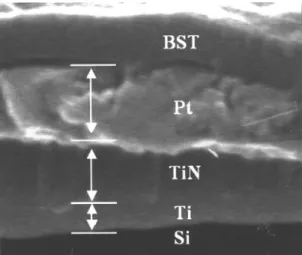
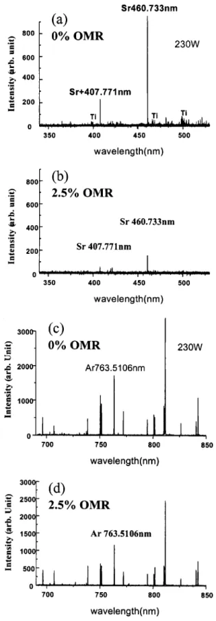
Figure 1 shows a cross-sectional FESEM micrograph of the BST/Pt/TiN/Ti/Si capacitor, with the BST film deposited at 300°C. Figure 2a reveals that the deposition rate of BST films drops dra-matically when oxygen is introduced into the sputtering ambient. Figure 2b indicates that the individual deposition rates of STO and BTO, show the same tendency as Fig. 2a. The optical emission spectra of both Ar and Sr plasma near the STO target were therefore analyzed during sputtering in pure Ar共0% OMR兲 and 2.5% OMR ambient, as shown in Fig. 3. The intensity decay of Sr plasma ( ⫽ 460.7 nm, from 0 to 2.5% OMR ambient兲 is much more promi-nent 共as shown in Fig. 3a, b兲 than that of Ar plasma ( ⫽ 763.5 nm, from 0 to 2.5% OMR ambient, as shown in Fig. 3c, d兲. That is, the generation of Sr plasma is suppressed in the presence of oxygen. The spectra of the STO target sputtered in even higher OMR show similar results. These spectra imply that sputtering SrTiO3molecules with Ar⫹ions in O2/Ar mixed ambient is diffi-cult. The oxygen ions are reported to induce reactive sputtering and form oxide on the target surface, and the presence of oxide de-creases the sputtering rate due to the increase in binding energy of the target surface.14-16 Ba/Sr ratios of BST films prepared on
SiO2/Si substrates were obtained by RBS, as shown in Fig. 4. The chemical composition of BST films sputtered in pure Ar ambient are Sr rich, and the Ba/Sr ratio is around 0.38/0.62. As indicated in Fig. 2b, the deposition rate of STO drops faster than that of BTO when oxygen is applied during sputtering. The Ba/Sr ratio thus increases in the O2/Ar mixed ambient and remains almost constant at 0.5/0.5 at a higher OMR共⭌5%兲 for fixed sputtering powers, as shown in Fig. 4. The dielectric constant of powder BST generally increases with Ba/Sr ratio, but that of thin BST films must be considered with several other factors, as discussed later.
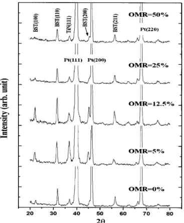
Figure 5 gives XRD patterns of BST films deposited at various OMR. Among the conditions studied, BST film deposited in 12.5% OMR exhibits a best crystallinity. Figure 6a and b indicates that the AES spectra of the BST films sputtered in 5 and 25% OMR, respec-tively. No oxygen atoms penetrate into the TiN/Ti layers under 5% OMR, as shown in Fig. 6a, but, intriguingly, the oxygen atoms pen-etrate into the TiN/Ti layers at 25% OMR, as shown in Fig. 6b. According to Fig. 5, the XRD intensity of TiN共111兲 is strongly en-hanced at 5% OMR, but that degrades above 12.5% OMR. The deposition rate of the BST films sputtered in 5% OMR is much lower than that in 0% OMR, so the longer thermal cycling time will enhance the crystallinity of TiN/Ti layers. On the other hand, Fig. 6b indicates the oxygen atoms penetrate the Pt film into TiN/Ti layers above 12.5% OMR, and thus the TiN/Ti layers react with the oxygen atoms, degrading this substrate. The crystallinity of the BST film is strongly affected by the qualities of Pt/TiN/Ti substrate, as reported in previous works.6,12,13Hence, the crystallinity of the BST films degrades above 12.5% OMR due to the TiN/Ti substrate damaged by the penetrating oxygen atoms.
The grain size of BST films is estimated from the full width at half-maximum共fwhm兲 of the XRD patterns, using the Scherrer for-mula共grain size ⬍100 nm兲
Dcal⫽ 0.89/共B ⫻ cos 兲 关1兴
where Dcalis the mean calculated grain size; is the X-ray wave-length共⬃0.154 nm兲; B is the fwhm of the XRD peak, and is the diffraction angle.17 The fwhm of the 共110兲 peak increases with OMR, and the calculated grain sizes are deduced by Eq. 1. Besides, an estimation of grain size from the fwhm is distorted by interfacial stress, so the calculated grain size should be modified by a factor obtained from a reference sample using FESEM imaging. The real grain size is around 8.3 nm at 5% OMR, as reported in previous work.18Thus, the calculated grain size should be multiplied by a factor of 1.22 to estimate the real grain sizes under the same sub-strate conditions.
In this study, relative grain sizes are much more important than absolute grain sizes. The small grain sizes of BST films decrease
Figure 1. Cross-sectional micrograph of BST/Pt/TiN/Ti/Si capacitor.
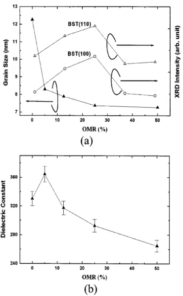
from 15 to 7 nm as OMR increases from 0 to 50%, as depicted in Fig. 7a, suggesting that films prepared at a higher OMR have a smaller grain size; other work has revealed a similar trend.7,11,19 Besides, Fig. 7a indicates that the strongest peaks of BST共100兲 and 共110兲 textures are obtained for the samples sputtered at 12.5% OMR. Moreover, Fig. 7b shows that the dielectric constant increases with OMR, reaching a maximum of 364 at 5% OMR, and then decreas-ing as OMR increases further. Figure 7a shows that best crystallinity occurs at 12.5% OMR and the grain size of the film shrinks as OMR increases. Many factors influence the dielectric constant of BST films such as composition, crystallinity, grain size, and interface quality. A high Ba/Sr ratio and good crystallinity enhances the po-larization of electric dipoles in a single grain,1,7,20but a small grain size tends to depress the dielectric constant, as reported in previous work.7,11,21Hence, the dielectric constant is inferred to increase as the crystallinity improves and as Ba/Sr ratio increases; but over 5% OMR the grain size effect dominates and the dielectric constant decreases as OMR further increases.
Figures 8a and b present the AFM micrographs of BST surface morphology: the films deposited at a higher OMR have smoother
surface. According to Fig. 8a and b, the root mean square 共rms兲 roughness (RRMS) for films deposited in pure Ar ambient is 5.06 nm, while that for films prepared at 12.5% OMR is 2.46 nm. Smaller grain and a lower film deposition rate at higher OMR may result in a smoother surface.
Figure 2. Deposition rate of共a兲 BST films, 共b兲 individual STO and BTO
films vs. OMR with sputtering power 230/175 W applied on STO/BTO tar-gets, respectively.
Figure 3. The plasma spectra of共a兲 Sr plasma in pure Ar ambient, 共b兲 Sr
plasma in 2.5% OMR,共c兲 Ar plasma in pure Ar ambient, and 共d兲 Ar plasma in 2.5% OMR, all detected near SrTiO3target.
Figure 9a indicates the leakage current density decreases as OMR increase. The leakage current of Pt/BST/Pt capacitors may be affected by three factors, namely, the oxygen stoichiometry in the BST films, surface morphology, and the grain boundary. First, the oxygen stoichiometries are different for the BST films prepared in various OMR ambient, according to the following reaction
Oo↔ Vo
••⫹ 2e⬘⫹ 1
2O2 关2兴
where Oo, Vo ••
, and e⬘represent the oxygen ion on its normal site, the oxygen vacancy and the electron, respectively. More oxygen vacancies yield a larger leakage current, causing a BST film form to act as an n-type semiconductor.22,23Second, smoother surface
mor-phology can prevent the lowering of barrier height by interfacial defects and reduce the local concentrated field to suppress the emis-sion current.24-26Third, a BST film, with a narrow bandgap of 3.2-4.0 eV, can normally be considered as semi-insulator or semicon-ductor, so the grain boundary scattering suppresses the current.27-29 The reduced grain size with higher OMR forms more grain bound-aries to decrease the leakage current. Hence, BST films deposited in higher OMR ambient exhibit compensation of oxygen vacancies, smoother interfaces and smaller grains, all of which reflect the de-crease of the leakage current. Figure 9b shows the tangent loss of BST films vs. OMR. Tangent loss proceeds by two mechanisms: resistive loss and relaxation loss.8In resistive loss case, energy is dissipated by mobile charges, and the tangent loss depends on the magnitude of leakage current; in relaxation loss case, energy is dis-sipated by relaxation of dipoles, and the tangent loss is proportional to the dielectric constant. Comparing Fig. 9a and b reveals that the trend of the tangent loss against OMR is similar to that of leakage current. Hence, the resistive loss dominates the tangent loss. Figure 9c indicates that the time-zero dielectric breakdown共TZDB兲 of the Pt/BST/Pt capacitor is enhanced by increasing OMR. BST films sputtered in higher OMR exhibit a higher breakdown field because of their smaller grain size and fewer oxygen vacancies.7,30 Figure 4. The Ba/Ba⫹ Sr ratio of BST films prepared in various OMR.
Figure 5. XRD patterns of BST films deposited on Pt/TiN/Ti/Si substrates
with various OMR.
Figure 6. AES spectra of BST films sputtered in共a兲 5% and 共b兲 25% OMR.
The BST films deposited in higher OMR have a longer lifetime, as indicated in Fig. 10. Time-dependent dielectric breakdown 共TDDB兲 is referred to as the resistance degradation of the dielectric ceramic, which slowly increases the leakage current under constant temperature and dc field stress.6,7,31 The mechanisms of resistance degradations in perovskite films may be generally categorized into the grain boundary model and the reduction model.31-33The grain boundary model suggests the presence of very large potential drops across the grain boundaries due to the boundaries’ high resistivities. The films with smaller grain sizes form more grain boundaries which the drops in voltage are shared, so the resistance degradation is suppressed. On the other hand, the reduction model suggests that oxygen vacancies and injection electrons cause resistance degrada-tion, which can thus be retarded by a smoother surface and lower oxygen vacancy concentration. Hence, BST films prepared with a higher OMR have a longer lifetime, which result can be attributed to the reduction of the grain sizes, compensation of oxygen vacancies and an improved interface.
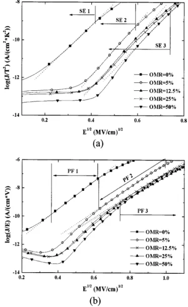
Figure 11 gives the C-V relationships of Pt/BST/Pt capacitors with various OMR. The conduction mechanisms of metal/BST/ metal capacitors are usually interpreted as Schottky emission 共SE, interface-limited conduction兲 at lower electric fields, and Poole-Frenkel emission 共PF, bulk-limited conduction兲 at higher
fields.9,25,26,34,35The leakage current governed by SE behavior is expressed as log共JSE/T 2兲 ⫽ ⫺q关 Bu⫺ 共qE/4do兲 1/2兴/共kT• ln 10兲 ⫹ log共A*兲 关3兴
where A*is the effective Richardson’s constant;Bis the potential barrier height at the surface;dis the dynamic dielectric constant of the ferroelectric material in the infrared region; q is the unit charge;
k is Boltzmann’s constant; T is temperature, and E is external
elec-tric field. The leakage current governed by PF behavior is expressed as
log共JPF/E兲 ⫽ ⫺q关t⫺ 共qE/do兲1/2兴/共kT • ln 10兲 ⫹ log B 关4兴 where B is a constant and t is the trapped energy level. If the conduction current is governed by PF, then a log(J/E) against E1/2 plot should be a straight line, the slope of which can be used to deduce the dynamic dielectric constant d.9,25,26,34,35Similarly, a log(J/T2) against E1/2plot can be made for SE. Figure 11a shows the SE plot and Fig. 10b shows the PF plot using the same experimental Figure 7. 共a兲 Grain sizes and relative XRD intensities of 共100兲 and 共110兲
textures for the BST films sputtered at various OMR;共b兲 dielectric constant of BST films prepared at various OMR.
Figure 8. AFM images of BST films deposited in共a兲 0% OMR (RRMS ⫽ 5.06 nm) and 共b兲 12.5% OMR (RRMS⫽ 2.46 nm).
current-voltage共I-V兲 data in various OMR. The dashed lines are the fitted results. However, the dynamic dielectric constant can be in-ferred from the optical dielectric constant for an ideal insulating film, and the optical dielectric constant is directly obtained from the
square of the refractive index n (opt⫽ n2).9,26,34,35Table I lists the static, dynamic, and optical dielectric constants of samples prepared at various OMR. In this work, the range of the dynamic dielectric constants (d) calculated by PF fitting is between 2.3 and 4.3, and that calculated by SE fitting is between 1.75 and 2.1. The range of the optical dielectric constant for BST films sputtered with various OMR, measured using an n & k analyzer with ⫽ 700 nm, is between 3.5 and 5.5. The consistency between dynamic (d) and the Figure 9. 共a兲 Leakage current density, 共b兲 tangent loss, and 共c兲 the TZDB
field of Pt/BST/Pt capacitors prepared in various OMR.
Figure 10. TDDB as a function of electric field of BST films deposited in
various OMR.
Figure 11. 共a兲 The log(J/T2) vs. E1/2plot showing SE fitting, and 共b兲 the log(J/E) vs. E1/2plot showing PF fitting for BST films prepared in various OMR.
Table I. The dynamic dielectric constant, static dielectric con-stants, and optical dielectric constants of BST films prepared in various OMR. OMR 共%兲 Dynamic dielectric constant Static dielectric constant Optical dielectric constant PF SE 0 2.30 2.09 330 3.53 5 3.19 1.77 364 4.66 12.5 4.18 1.91 317 5.29 25 4.18 2.01 293 4.28 50 4.23 1.98 265 4.34
optical dielectric constant (opt) is enough to trust the curve fitting, even thoughdandoptrevealed some deviation, perhaps due to the fluctuations of material’s density and deformation of its lattice.
Figure 11a and b indicate that Pt/BST/Pt capacitor sputtered at 0% OMR exhibits SE/PF under/above 160 kV/cm, as denoted in the SE 1/PF 1 regions. Figure 11b reveals that log(J/T2) curves for 5, 12.5, 25, and 50% OMR are independent of the applied field共E兲 up to 160 kV/cm, possibly because of the dielectric relaxation of BST films; the curves then increase linearly with E1/2above 160 kV/cm. SE 2 and PF 2 regions show SE/PF behaviors under and above 360 kV/cm in 5% OMR, respectively. SE and PF regions in higher OMR 共⭌12.5%兲 are SE 3 and PF 3 regions, respectively.
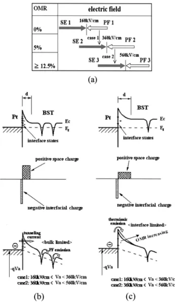
Figure 12a rearranges the tendencies of the leakage mechanisms, and it reveals that the applied-field boundary of SE/PF linear fitting shifts to a higher field as OMR increases. In case 1, the fitting boundary shifts from 160 kV/cm 共SE 1/PF 1兲 to 360 kV/cm 共SE 2/PF 2兲, as OMR increases from 0 to 5%, and, in case 2, it shifts to 560 kV/cm 共SE 3/PF 3兲, when OMR is equal to or larger than 12.5%. The electron energy bands of the Pt/BST interface are ap-plied to explain the mechanisms of leakage, as presented in Fig. 12b and c. As mentioned above, the BST films can be treated as an n-type semiconductor, and the space charge density of the interfacial depletion region is assumed to be almost equal to the concentration
of oxygen vacancies. The relationship between the barrier thickness,
d, of the interfacial depletion region and the oxygen vacancy
con-centration can be derived as
d1/d2⫽兵NVO2/NVO1⫻ 关1 ⫹ kT/⌬ ⫻ ln共NVO1/NVO2兲兴其0.5 关5兴 where NVO is the concentration of oxygen vacancies; k is Boltz-mann’s constant; T is temperature, and⌬ is the work function dif-ference between Pt and BST. Equation 5 reveals that decreasing the concentration of oxygen vacancies increases the barrier thickness, d, of the interfacial depletion region.36Figure 12b indicates that the BST films sputtered in pure Ar or in lower OMR ambient have more oxygen vacancies and a rougher surface than those sputter in higher OMR ambient, yielding a higher interfacial space charge concentra-tion and many interface states to increase the opportunity of tunnel-ing. Furthermore, the magnitude of the leakage current is governed by the balance among the tunneling current, trapping and detrapping rate. Thus, increasing the applied field induces the field-assisted emission of trapped charged carriers 共Poole-Frenkel effect兲, such that the leakage current will be governed by PF emission rate. The bulk-limited mechanism therefore dominates the leakage current at lower OMR and higher applied field. Figure 12c shows that increas-ing OMR yields fewer interface states, a lower space charge density in the interfacial depletion region and fewer trapping states, by caus-ing a smoother interface and compensatcaus-ing oxygen vacancies. Equa-tion 5 states that a lower space charge density in the interfacial depletion region results in a thicker barrier, and the presence of fewer interface states greatly reduces the opportunity for tunneling. Hence, thermionic emission共SE behavior兲 is the dominant mecha-nism of injecting electrons in higher OMR. Consequently, consider-ing cases 1 and 2 of Fig. 12a, the mechanism of the leakage current changes from bulk limited emission共PF兲 to interface limited emis-sion共SE兲 as OMR increases.
Conclusions
The deposition rate of low temperature sputtered BST decreases as OMR increases, due to the formation of oxide on the target sur-face by oxygen ions. Introducing proper oxygen gas during sputter-ing improves the crystallinity and surface roughness of BST films and changes the Ba/Sr ratio, but decreases the grain size. In addition, the excessive OMR共⬎12.5%兲 degrades the crystallinity of BST film due to the TiN/Ti substrate damaged by the penetrations of the oxy-gen atoms. The dielectric constant is a trade-off determined by com-positions, crystallinity and grain size, and the maximum dielectric constant is 364 at 5% OMR. Films prepared at higher OMR have a smaller leakage current density, a lower tangent loss and a longer lifetime, due to compensation of oxygen vacancies, a smother sur-face morphology and voltage shared by smaller grains.
This study attributed the leakage mechanisms of the Pt/BST/Pt capacitor to共SE兲/PF at lower/higher applied field. Part of the PF region changes to SE behavior if OMR increases. In other words, the applied field boundary between SE and PF fittings shifts to a higher field as OMR increases, and this observed I-V behavior is explained by the decrease in the number of interface states and the compensation of oxygen vacancies.
Acknowledgments
This work was supported in part by the Republic of China Na-tional Science Council共R.O.C. NSC兲 under contract NSC 90-2216-E-009-032 and Energy Commission Ministry of Economic Affairs, R.O.C. Thanks are also due to the Semiconductor Research Center 共SRC兲 in National Chiao Tung University and the National Nano Device Laboratory 共NDL兲 of the R.O.C. NSC for their technical support.
National Chiao Tung University assisted in meeting the publication costs of this article.
Figure 12. 共a兲 The range of applied field for SE/PF mechanism in various
OMR ambient, and the diagrams of the electron energy band in共b兲 pure Ar or lower OMR ambient and共c兲 higher OMR ambient.
References
1. T. Kuoiwa, Y. Tsunenine, T. Horikawa, T. Makita, J. Tanimura, N. Mikami, and K. Sato, Jpn. J. Appl. Phys., Part 1, 33, 5187共1994兲.
2. A. Qutzourhit, J. U. Trefny, T. Kito, B. Yarar, A. Naziripour, and A. M. Hermann, Thin Solid Films, 259, 218共1995兲.
3. S. Onishi, K. Hamada, K. Ishhara, Y. Ito, S. Yokoyama, J. Kudo, and K. Sakiyama, Tech. Dig. - Int. Electron Devices Meet., 1994, 843.
4. S. R. Summerfelt, Thin Film Ferroelectric Materials and Devices, R. Ramesh, Editor, p. 31, Kluwer Academic Publishers, Dordrecht共1997兲.
5. S. Yamamichi, P.-Y. Lesaicherre, H. Yamaguchi, K. Takemura, S. Sone, H. Yabuta, K. Sato, T. Tamura, K. Nakajima, S. Ohnishi, K. Tokashiki, Y. Hayashi, Y. Kato, Y. Miyasaka, M. Yoshida, and H. Ono, Tech. Dig. - Int. Electron Devices Meet., 1995, 119.
6. C. C. Hwang, M. H. Juang, M. J. Lai, C. C. Jaing, J. S. Chen, S. Huang, and H. C. Cheng, Solid-State Electron., 45, 121共2001兲.
7. M. S. Tsai, S. C. Sun, and T. Y. Tseng, J. Appl. Phys., 82, 3482共1997兲. 8. M. S. Tsai and T. Y. Tseng, J. Electrochem. Soc., 145, 2583共1998兲. 9. M. S. Tsai and T. Y. Tseng, J. Electrochem. Soc., 145, 2853共1998兲.
10. C. R. Cho, Sook II Kwun, T. W. Noh, and M. S. Jang, Jpn. J. Appl. Phys., Part 1, 36, 2196共1997兲.
11. J. Lee, Y. C. Choi, and B. S. Lee, Jpn. J. Appl. Phys., Part 1, 36, 3644共1997兲. 12. C. C. Hwang, C. C. Jaing, M. J. Lai, J. S. Chen, S. Huang, M. H. Juang, and H. C.
Cheng, Electrochem. Solid-State Lett., 3, 563共2000兲.
13. T. H. Teng, C. C. Hwang, M. J. Lai, S. C. Huang, J. S. Chen, C. C. Jaing, and H. C. Cheng, Mater. Res. Soc. Symp. Proc., 596, 37共2000兲.
14. D. L. Smith D, Thin-Film Deposition Principles and Practice, p. 480, McGraw-Hill Inc., New York共1995兲.
15. S. B. Krupanidhi, H. Hu, and G. R. Fox, Ferroelectric Thin Films: Synthesis and Basic Properties, C. Paz de Araujo, J. F. Scott, G. W. Taylor, and S. B. Krupanidhi, Editors, p. 93, Gordon and Breach Publishers, Philadelphia PA共1996兲. 16. J. Roth, In Sputtering by Particle Bombardment II, R. Behrish, Editor, p. 91,
Springer-Verlag, New York共1983兲.
17. B. D. Cullity, Elements of X-Ray Diffraction, p. 102, Addison-Wesley Inc., Read-ing, MA共1978兲.
18. C. C. Hwang, M. J. Lai, C. C. Jaing, J. S. Chen, S. Huang, M. H. Juang, and H. C. Cheng, Jpn. J. Appl. Phys., Part 2, 39, L1314共2000兲.
19. T. Horikawa, N. Mikami, T. Makita, J. Tanimura, M. Kotaoka, K. Sato, and M. Nunoshta, Jpn. J. Appl. Phys., Part 1, 32, 4126共1993兲.
20. K. Takemura, S. Yamamichi, P. Y. Lesaicherre, K. Tokashiki, H. Miyamoto, H. Ono, Y. Miyasaka, and M. Yoshida, Jpn. J. Appl. Phys., Part 1, 34, 5224共1995兲. 21. K. Okazaki and K. Nagata, J. Electron. Commun. Soc. Jpn.,, C53, 815共1970兲. 22. R. M. Waser, J. Am. Ceram. Soc., 72, 2234共1989兲.
23. D. M. Smyth, M. P. Harmer, and P. J. Peng, J. Am. Ceram. Soc., 72, 2276共1989兲. 24. I. Stolichnov, A. Tagantsev, N. Setter, S. Okhonin, P. Fazan, J. S. Cross, and M.
Tsukada, J. Appl. Phys., 87, 1925共2000兲.
25. C. S. Hwang, B. T. Lee, C. S. Kang, J. W. Kim, K. H. Lee, H. J. Cho, H. Horii, W. D. Kim, S. I. Lee, Y. B. Roh, and M. Y. Lee, J. Appl. Phys., 83, 3703共1998兲. 26. C. S. Hwang, B. T. Lee, C. S. Kang, K. H. Lee, H. J. Cho, H. Hideki, W. D. Kim,
S. I. Lee, and M. Y. Lee, J. Appl. Phys., 85, 287共1999兲. 27. W. Heywang, J. Mater. Sci., 6, 1214共1971兲.
28. G. T. Mallick, Jr. and P. R. Emtage, J. Appl. Phys., 39, 3088共1968兲. 29. G. E. Pike and C. H. Seager, J. Appl. Phys., 50, 3414共1979兲.
30. L. H. Parker and A. F. Tasch, IEEE Circuits Devices Mag., 1990, 17共Jan兲. 31. M. S. Tsai and T. Y. Tseng, IEEE Trans. Compon., Packag. Manuf. Technol., Part
A, 23, 128共Mar 2000兲.
32. R. Waser, R. T. Baiatu, and K. H. Hardtl, J. Am. Ceram. Soc., 73, 1645共1990兲. 33. H. Y. Lee and K. L. Lee, IEEE Trans. Compon., Hybrids, Manuf. Technol., 4, 443
共1984兲.
34. Y. B. Lin and J. Y. Lee, J. Appl. Phys., 87, 1841共2000兲. 35. R. M. Hill, Thin Solid Films, 8, R21共1971兲.
36. M. S. Tyagi, Metal-Semiconductor Schottky Barrier Junctions and Their Applica-tions, B. L. Sharma, Editor, p. 27, Plenum Press, New York共1984兲.