IEEE TRANSACTIONS ON MAGNETICS, VOL. 47, NO. 10, OCTOBER 2011 2519
Magnetic Interaction in Domain Wall Depinning at Square
Notch and Antinotch Traps
L. J. Chang , Y. D. Yao , Pang Lin , and S. F. Lee
Institute of Physics, Academia Sinica, Taipei 115, Taiwan
Department of Materials Science and Engineering, National Chiao Tung University, Hsinchu 300, Taiwan Institute of Applied Science and Engineering, Fu Jen University, Taipei 242, Taiwan
In this paper, we report on domain wall (DW) pinning and depinning behavior using square notch and antinotch in NiFe nanowires. The presence of the DW in the samples was probed experimentally from focus magneto-optical Kerr effect (MOKE) measurement and anisotropic magnetoresistance (AMR). Pinning strengths as well as distribution of depinning field were measured. DW traps with antinotches were found to be more effective than notches, and the DW kept its structure during the depinning processes. Simulations of the magnetization orientation agreed with our results.
Index Terms—Current-induced domain wall motion, domain wall (DW).
I. INTRODUCTION
T
HE domain wall (DW) pinning and propagation in fer-romagnetic nanowires has become the focus of investi-gations. Several of the practical applications on domain-wall-based devices including both spintronic logic [1] and magnetic memory devices [2], [3] have been proposed. Such devices of magnetic technology require high level of control of DW prop-agation since the logic information is encoded in the orienta-tion of magnetizaorienta-tion in the magnetic nanowires. The artificial structures of notches in the magnetic nanowires have been in-troduced for pinning DWs [4]. The locations of DWs were be-lieved to be well defined in the trap along the wire. The dis-tance of the pinned DWs constitutes essentially the minimum separation size between the bit units. Recently, the DW pin-ning behaviors at notches have attracted intense investigations. It has been shown that the DW depinning field increases as the notch depth increases [4]. Double DW nucleation was found in deep notch samples and needs special attention in structure de-signs [5]. The chirality of the DW also influences the strength of pinning effect for asymmetric notches [6]–[9]. It was shown that the pinning effect depended on how different orientation of transverse DWs interacted with the trap and indicated the dis-tribution of kinetic depinning field was due to the oscillatory motion of DW [10]–[12]. Very recently, Akerman et al. [13] studied the stochastic behavior of the DW depinning in NiFe nanowires with different types of notches. It has been shown that two type of notches, square shallow and elliptical deep ones, presented higher probability of pinning. However, these mea-surements also showed that the dispersion in the values of de-pinning field came together with variations in the anisotropic magnetoresistance (AMR) profile. The standard deviation of de-pinning field depended on the distorted structure of DW ap-proaching the notch. In this work, we investigate the behavior of DW depinning at symmetrical antinotch and notch in NiFeManuscript received February 21, 2011; accepted May 10, 2011. Date of current version September 23, 2011. Corresponding author: S. F. Lee (e-mail: [email protected]).
Color versions of one or more of the figures in this paper are available online at http://ieeexplore.ieee.org.
Digital Object Identifier 10.1109/TMAG.2011.2157114
Fig. 1. SEM image of (a) antinotch and (b) notch nanowires. MOKE signal (c) antinotch wire with 800 nm and 350 nm and (d) notch wire with 300 nm and 600 nm.
nanowires. The AMR profile and focus magneto-optical Kerr effect (MOKE) data have been measured. We have observed the process of propagation of DWs traveling through the trap. The probability of pinning in each sample and the variation in AMR profile depend on the structure of the DW. We have also analyzed the results of magnetic force microscopy (MFM) and micromagnetic simulations and showed they are consistent.
II. EXPERIMENTALMETHODS
The submicrometer wires with notch and antinotch struc-ture were fabricated by electron-beam lithography and liftoff technique. NiFe samples were deposited by direct current (dc) magnetron sputtering on Si substrates. The wires were 20 nm thick, 800 nm wide, and 40 m long. A notch 300 nm deep and with various widths, or an antinotch with 300- or 800-nm height and various widths were prepared. A diamond shape pad at one end of the sample was designed to ensure the DW nucleation at low field. Four-point probes with Au/Cu electrode leads were then fabricated by a second liftoff process for resis-tance measurements. Fig. 1(a) and (b) shows scanning electron microscopy images of our samples with antinotch [Fig. 1(a)]
2520 IEEE TRANSACTIONS ON MAGNETICS, VOL. 47, NO. 10, OCTOBER 2011
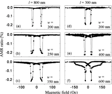
Fig. 2. AMR signal for antinotch nanowires with different geometries parameters.
and notch [Fig. 1(b)]. To understand the DW motion charac-teristics, we used magnetoresistance (MR) and longitudinal micro-MOKE techniques. The 5- m diameter laser spot in MOKE measurements was focused on the center of the notches or antinotches. The magnetic field was applied along the long axis of wires. Magnetoresistance changes of the samples were measured with a constant 10- A measuring current.
III. RESULTS ANDDISCUSSIONS
The hysteresis loops are presented in Fig. 1(c) for antinotch wire with 800 nm and 350 nm and Fig. 1(d) for notch wire with 300 nm and 600 nm. These data were taken with the laser spot centered over the artificial trap site. We ob-serve that each hysteresis loop contains two switching steps. In Fig. 1(c), the first step at field value about 21 Oe is in-terpreted as the DW propagating from the nucleation pad and entering into the antinotch. The second step occurs at 36 Oe, which indicates that the DW depinning from the trap occurs. The AMR profile is correlated in field with the results measured from MOKE. However, in Fig. 1(d), the field value of the second step at 123 Oe is larger than depinning field of AMR data. We suggest that these behaviors correspond to the double nucleation at the side of the notch after the depinning process.
In Fig. 2, we present the AMR signal for antinotch nanowires with different geometries parameters. We observed that the vari-ations of the AMR profiles were markedly sensitive to both the width and the height of the antinotches. Shown in Fig. 2(a)–(c) are the AMR data for the samples with fixed length of 800 nm as a function of width . All the AMR profiles showed single transition between the first falling edge (defined as the propagation field ) and rising edge (defined as the depin-ning field ). This implies the stability of the DW structure during the depinning process. We have also found that the value of increases with increasing . It indicates that the stability of the pinned DW strongly depends on both width and height of antinotch. For the fixed 300 nm samples, as seen in
Fig. 3. Probability of pinning for each type of samples.
Fig. 2(d)–(f), the data of narrow present similar transition be-havior with the 800 nm. For the broad antinotch in Fig. 2(f), however, we observe double transition steps, which indicate that there are two principle depinning fields from each pinned DW structure. This is due to the fact that the depinning field of nanowires sensitively depends on the DW structure when the DW approaches the antinotch. We have also performed experi-ments for 300 nm 250 and 350 nm. The experimental results are not shown here but they exhibit the similar behavior with the 300 nm 200 nm sample.
The probability of DW pinning for NiFe wires with different type of samples obtained in the AMR experiment is plotted in Fig. 3. The AMR signal is dependent on the relative orientation between the local magnetization and current direction. For the pinning events, a sharp drop in AMR signal is observed. The DW was trapped at the notch or antinotch. For the nonpinning events, we cannot find variation of resistance in the AMR curve. The data take into account 100 measurements for every wire. For the antinotch wires, as seen in Fig. 3(a), we observe that the pinning probability increases significantly with increasing width for both lengths of traps. Furthermore, the wires with tall trap 800 nm show more effective pinning ability than the samples with 300 nm. In Fig. 3(b), the probability of pinning in notch wires with depth 200 and 300 nm and width 200, 400, and 600 nm displays a gradual change with the width of notch and the pinning probability is almost independent to the depth of notch. From these measurements, we can conclude that the tall and wide antinotch is the good pinning structure. Also wide notch of both depths shows effective pinning for DW.
In Fig. 4, we present the distributions of DW depinning field measured in all samples. The graphs are plotted with 100 mea-surements for every type of notch. These data give us an ideal of how many major there are in each sample. When depin-ning occurs at several major values of fields, there are different configurations of the DW traveling through the artificial trap. Antinotch ( 800 nm 350 nm) and notch ( 300 nm 200 nm) show only one major depinning field around 34 Oe and 53 Oe, respectively, as seen in Fig. 4(a) and (c). This implies that the DW has a single depinning process. For
CHANG et al.: MAGNETIC INTERACTION IN DOMAIN WALL DEPINNING AT SQUARE NOTCH AND ANTINOTCH TRAPS 2521
Fig. 4. Probability distributions of the depinning field of a DW in each type of the samples.
wide antinotch [Fig. 4(b)], and notches in Fig. 4(d) and (e), there exhibits two distinct depinning fields. The notch sample with 200 nm 600 nm in Fig. 4(f) shows three dif-ferent depinning clusters. We suggest that these split of cor-responding to different metastable states of the DW inside the trap.
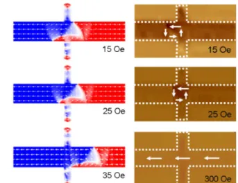
To better understand the depinning process, we carried out micromagnetic simulations for all the samples in this research. The OOMMF simulation software package from the National Institute of Standards and Technology (NIST) [14] was used. The parameters used in the simulation are saturation magneti-zation 8.6 10 A/m, exchange energy constant 1.3
10 J/m, anisotropy constant 0 J/m , and cell size 5 nm. From the phase diagram of magnetization switching be-havior of a magnetic nanowire as functions of geometrical pa-rameters, a vortex DW was propagating from the nucleation pad and entering into the trap. Fig. 5 shows the simulated depinning process of antinotch wire with 800 nm, 350 nm on the left, and the right sequence displays the corresponding magnetic states obtained from the MFM images. For the results of simu-lations, the structure of vortex DW does not show distortion or double nucleation during the pinning and depinning processes. In the top one of MFM images, when the field is 15 Oe, the DW arrives on the left side of antinotch. The middle MFM image shows the DW was trapped in the antinotch. When the DW is depinned from the antinotch, it moves away quickly and cannot be measured by MFM. The MFM image is in direct agreement with the simulation results. These results show the large length of antinotch is an ideal structure for pinning DW in nanowires.
Fig. 5. Micromagnetic simulation of the magnetic states of the 20-nm-thick NiFe antinotch wire with 800 nm, 350 nm, and the corresponding MFM image.
IV. SUMMARY
A combination of MOKE measurement, AMR, micromag-netic simulation, and MFM image has allowed a systematic study in the DW pinning and depinning behavior at square notch and antinotch in NiFe nanowires. We found that probabilities of pinning are sensitive to geometry parameter of antinotch. In tall and wide antinotch wire, the depinning field shows one major value and very good pinning probability.
ACKNOWLEDGMENT
This work was supported by the National Science Council and the Academia Sinica, Taiwan.
REFERENCES
[1] D. A. Allwood, G. Xiong, C. C. Faulkner, D. Atkinson, D. Petit, and R. P. Cowburn, Science, vol. 309, p. 1688, 2005.
[2] S. S. P. Parkin, M. Hayashi, and L. Thomas, Science, vol. 320, p. 190, 2008.
[3] M. Hayashi, L. Thomas, R. Moriya, C. Rettner, and S. S. P. Parkin,
Science, vol. 320, p. 209, 2008.
[4] C. C. Faulkner, M. D. Cooke, D. A. Allwood, D. Petit, D. Atkinson, and R. P. Cowburn, J. Appl. Phys., vol. 95, p. 6717, 2004.
[5] L. K. Bogart, D. S. Eastwood, and D. Atkinson, J. Appl. Phys., vol. 104, 2008, 033904.
[6] L. K. Bogart, D. Atkinson, K. O’Shea, D. McGrouther, and S. McVitie,
Phys. Rev. B, vol. 79, 2009, 054414.
[7] D. Petit, A.-V. Jausovec, D. Read, and R. P. Cowburn, J. Appl. Phys., vol. 103, 2008, 114307.
[8] D. Petit, H. T. Zeng, J. Sampaio, E. Lewis, L. O’Brien, A.-V. Jausovec, D. Read, R. P. Cowburn, K. J. O’Shea, S. McVitie, and J. N. Chapman,
Appl. Phys. Lett., vol. 97, 2010, 233102.
[9] K. He, D. J. Smith, and M. R. McCartney, Appl. Phys. Lett., vol. 95, 2009, 182507.
[10] D. Petit, A.-V. Jausovec, H. T. Zeng, E. Lewis, L. O’Brien, D. Read, and R. P. Cowburn, Appl. Phys. Lett., vol. 93, 2008, 163108. [11] D. Petit, A.-V. Jausovec, H. T. Zeng, E. Lewis, L. O’Brien, D. Read,
and R. P. Cowburn, Phys. Rev. B, vol. 79, 2009, 214405.
[12] E. R. Lewis, D. Petit, L. O’Brien, A.-V. Jausovec, H. T. Zeng, D. E. Read, and R. P. Cowburn, Appl. Phys. Lett., vol. 98, 2011, 042502. [13] J. Akerman, M. Muñoz, M. Maicas, and J. L. Prieto, Phys. Rev. B, vol.
82, 2010, 064426.