2168-6734 (c) 2015 IEEE. Translations and content mining are permitted for academic research only. Personal use is also permitted, but republication/redistribution requires IEEE permission. See http://www.ieee.org/publications_standards/publications/rights/index.html for more information.
This article has been accepted for publication in a future issue of this journal, but has not been fully edited. Content may change prior to final publication. Citation information: DOI 10.1109/JEDS.2016.2537359, IEEE Journal of the Electron Devices Society
> REPLACE THIS LINE WITH YOUR PAPER IDENTIFICATION NUMBER (DOUBLE-CLICK HERE TO EDIT) < 1
Abstract— A novel bonding approach for flexible substrate vertical stacking is proposed in this paper. Unlike the traditional anisotropic conductive/non-conductive paste/film used in flexible substrate bonding, the metal thin film is adopted as bonding material in this approach. Experiment results show that the novel bonding approach has good electrical properties and reliability performances. The innovative bonding approach is considered a breakthrough of the traditional restrictions in flexible substrates, including I/O pitch, electrical reliability, and bonding conditions. This development is expected to contribute to the fabrication of future flexible substrate stacking.
Index Terms—Flexible substrate, 3D integration, Fine-pitch application, Bonding.
I. INTRODUCTION
n recent years, the requirements for flexible, bendable, and wearable electronic products has been growing in biomedical, mobile, entertainment, and Internet-of-Things industries. Therefore, electronics device and circuit are expected to integrate on the flexible substrate to achieve these goals. According to the demand of products, various flexible heterogeneous integrated electronic package technologies are developed, such as Chip-on-Flex (CoF) and Chip-in-Flex (CiF). A more advanced technique is to manufacture the electronic device on the flexible substrate directly [1]. With the demand of such circuit functionality, the flexible substrate 3D stacking, Flex-on-Flex (FoF), is the imperative direction in the future. Among these manufacturing technologies, bonding approach is the key to better electrical property, structure reliability, and bonding strength.
In conventional flexible substrate bonding approaches, anisotropic conductive film (ACF) or non-conductive paste (NCP) is widely used due to their low bonding temperature and good flexibility property. However, several challenges exist in these approaches. The appropriate curing process is required and a significant factor in the overall electrical performance of joints [2]. Besides that, bump pitch is difficult to scale down to increase interconnect density. In addition, adhesive resin properties affect the reliability and stability of the structure [3]. Therefore, some specific materials [4, 5] and bonding approach [6] are used to improve the traditional methods, but further
This work was supported in part by the Ministry of Education in Taiwan under the ATU Program, in part by the Ministry of Science and Technology through Grant MOST 103-2221-E-009-173-MY3 and Grant MOST 103-2221-E-009-193-MY3, and in part by the NCTU-UCB I-RiCE program under Grant MOST 105-2911-I-009-301.
Yu-Chen Hu and Kuan-Neng Chen are with the Department of Electronics Engineering, National Chiao Tung University, Hsinchu 30050, Taiwan (e-mail: [email protected]).
studies are still required.
In this letter, a novel bonding approach using metal thin film is proposed to overcome the current ACF/NCP usage restrictions and is suitable for application in the flexible substrate. This innovative bonding approach does not only retain the low temperature bonding and flexibility property but also achieves ultra-fine pitch and stable reliability. Sn/In and Cu are selected as the bond materials due to their low melting point and good ductility. Electrical and reliability results show that it is a promising solution to potentially replace the conventional bonding approaches.
II. COMPARISON WITH CONVENTIONAL FLEXIBLE SUBSTRATE BONDING APPROACHES
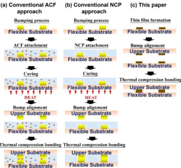
In the conventional ACF/NCP bonding approaches, electroplating bump process, generally Au, is first fabricated on the substrate, followed by attaching ACF/NCP as the interlayer to bind the upper and lower substrates. The next step curing is the most critical process, where the optimized conditions are based on the result of differential scanning calorimeter (DSC) or Fourier transform infrared (FTIR) [7, 8]. Finally, thermal compression bonding is applied.
ACF/NCP approaches use different bonding mechanisms from direct bonding in 3D integration. ACF consists of conductive particles and adhesive polymer resin. After bonding, the conductive particles act as an electrical path between two bumps, as shown in Fig. 1(a). Accordingly, a trade-off issue, which is the conductive particle density, exists in ACF approach. If the conductive particle density is too high, electrical short circuit issue will occur between two adjacent bumps due to the bridging phenomenon. On the contrary, the resistance could increase if with a small amount of conductive particles. The conductive particle size also limits the fine pitch [9]. NCP is developed to simplify and to achieve fine pitch interconnections. Unlike ACF, NCP approach has no conductive particles. Two opposite bumps are bonded directly, as shown in Fig. 1(b). Larger bonding area is required when using NCP as compared to ACF because the bonding contact area involved is the entire bump surface instead of just random conductive particles. However, NCP trapping issue which causes unstable reliability and increased resistance exists at the interface between two bumps [10].
Comparing with the above conventional ACF/NCP approaches, our proposed approach in Fig. 1(c) does not require the extra curing process and pre-treatment. By using a very thin bonding pad of less than 1μm-thickness, we are able to realize the flexible substrate bonded structure that could tolerate under bending condition. In addition, the approach can achieve ultra-fine pitch with no adhesive trapping issue. With the
A Novel Bonding Approach and Its Electrical
Performance for Flexible Substrate Integration
Yu-Chen Hu, and Kuan-Neng Chen, Senior Member, IEEE
2168-6734 (c) 2015 IEEE. Translations and content mining are permitted for academic research only. Personal use is also permitted, but republication/redistribution requires IEEE permission. See http://www.ieee.org/publications_standards/publications/rights/index.html for more information.
This article has been accepted for publication in a future issue of this journal, but has not been fully edited. Content may change prior to final publication. Citation information: DOI 10.1109/JEDS.2016.2537359, IEEE Journal of the Electron Devices Society
> REPLACE THIS LINE WITH YOUR PAPER IDENTIFICATION NUMBER (DOUBLE-CLICK HERE TO EDIT) < 2
validation of electrical performance and reliability test, this approach can replace the conventional method in 3D flexible substrate integration scheme.
III. EVALUATION OF THIN FILM BONDING
A 75-μm Kapton polyimide (PI) flexible substrate was cut to 6 cm * 6 cm size and cleaned in acetone with ultrasonic to remove particles and organic contaminations. 300-nm Cu thin film was deposited and 10-nm Ti was sandwiched in between Cu and PI substrate as an adhesive layer. To achieve low temperature bonding, 20-nm Ni film, 300-nm Sn film and 300-nm In film were deposited sequentially on the other PI substrate. Different bonding pads, from sizes of 5 μm to 100 μm, were formed on the PI substrate to evaluate the electrical properties. Fig. 2(a) shows that we successfully demonstrate ultra-fine pitch bond pads with 5-μm-diameter and 10-μm-pitch, which completely surpass the minimum pitch size formed by traditional bonding approaches [11] without any electrical short concern. Thermal compression bonding was applied to integrate two face-to-face PI substrates without surface treatment or curing process. These samples were bonded at 100 N force and 170 °C for 30 min. According to the Sn-In binary system, Sn-In eutectic liquid phase could form when bonding temperature is over 118 °C, which allows the realization of a lower bonding temperature as compared to traditional approaches. The bonded structure was analyzed by SEM, TEM, and EDX for element analysis and microstructure observation.
Figs. 2(b) and 2(c) present well-bonded cross-sectional SEM and TEM images of submicron bonded layer without voids and cracks. Base on Fig. 2(d) EDX analysis result, Cu is diffused at a higher speed to In/Sn side, which also proves the well-bonded structure after diffusion.
IV. ELECTRICAL MEASUREMENT AND RELIABILITY To examine the flexibility of this approach, specific contact resistance performance was measured by Kelvin structure with flat and bending radius-30 mm measurements, respectively. Fig. 3 shows the electrical property results. The novel bonding approach has a stable specific contact resistance of approximately 2.5×10⁻⁷ Ω-cm2 under both states. The two almost identical resistance values show that good metal thin film ductility can be used for bonding application.
In order to evaluate the reliability of the proposed approach, thermal cycling test (TCT) and un-bias highly accelerated stress test (un-bias HAST) are adopted. TCT was performed with temperature range from -55 to 125 °C (JESD22-A104B). As shown in Fig. 4(a), after 500 thermal cycling loop executions, the resistance is only slightly increased.
Furthermore, the un-bias HAST was set to 130 °C, 85 % for 96 hours. The results of un-bias HAST in Fig. 4(b) indicates that the resistance variance is small and even decrease slightly. In the above reliability tests, specific contact resistance maintained the same order (~10-7 Ω-cm2), showing the novel bonding approach is stable. Comparing with the conventional Fig. 1. Schematic diagrams of (a) conventional ACF approach, (b)
conventional NCP approach, and (c) metal thin film approach proposed in this paper.
Fig. 2. (a) SEM image of the ultra-fine pitch In/Sn bonding pad with 5-µm diameter and 10-µm pitch. (b) SEM image of metal bonded layer without voids and cracks. (c) XTEM of bonded structure. (d) Corresponding composition with Cu/In/Sn layers in Fig. 2(c).
Fig. 3. Measured specific contact resistance of bonded flexible substrate structure at alternate flat and bending states.
2168-6734 (c) 2015 IEEE. Translations and content mining are permitted for academic research only. Personal use is also permitted, but republication/redistribution requires IEEE permission. See http://www.ieee.org/publications_standards/publications/rights/index.html for more information.
This article has been accepted for publication in a future issue of this journal, but has not been fully edited. Content may change prior to final publication. Citation information: DOI 10.1109/JEDS.2016.2537359, IEEE Journal of the Electron Devices Society
> REPLACE THIS LINE WITH YOUR PAPER IDENTIFICATION NUMBER (DOUBLE-CLICK HERE TO EDIT) < 3
approach, the specific contact resistance of metal thin film bonding is almost at the same order but even better [9].
Overall, this novel bonding approach is developed and investigated on the electrical and reliability. Electrical properties of this approach are better than those of current methods, indicating this novel approach has the potential for flexible substrate vertical assembly in the future.
V. CONCLUSION
A well-bonded flexible substrate using conventional approach needs considerations, such as bonding temperature, bonding pressure, bump height, curing temperature, and pitch. In this letter, a novel bonding approach applied in the flexible substrate using metal thin film is proposed to simplify the process. Electrical property under the bending condition is the same as a flat condition with metal ductility. Reliability tests also indicate a stable electrical characteristic. This bonding approach achieves ultra-fine pitch, less reliability issue factors and simple process, which can be applied in the flexible substrate 3D stacking such as Flex-on-Flex and Chip-on-Flex.
REFERENCES
[1] T. He, Y. Yi, L. Cheng, M. A. Mohammad, and R. Tian-Ling, "Flexible, transparent single-layer graphene earphone," in Proc. IEEE IEDM, San Francisco, CA, Dec. 2014, pp. 15.3.1-15.3.4. DOI: 10.1039/C4RA16047A
[2] M. J. Rizvi, Y. C. Chan, C. Bailey, H. Lu, and A. Sharif,, "The effect of curing on the performance of ACF bonded chip‐on‐flex assemblies after thermal ageing," Soldering & Surface Mount Technology, vol. 17, no. 2, pp. 40-48, Feb. 2005. DOI: 10.1108/09540910510597492
[3] K. Yoo-Sun, K. Seung-Ho, S. Jiwon, and P. Kyung-Wook, "Reliability improvement of solder anisotropic conductive film (ACF) joints by controlling ACF polymer resin properties," in Proc. 65th IEEE ECTC , San Diego, CA, May 2015, pp. 1813-1817. DOI: 10.1109/ECTC.2015.7159845
[4] K. Tae-Wan, L. Sang-Hoon, and P. Kyung-Wook, "Effect of aligned nanofiber in nanofiber solder anisotropic conductive films (ACFs) on the solder ball movement for flex-on-flex (FOF) assembly," in Proc. 64th
IEEE ECTC , Orlando, FL, May 2014, pp. 271-278. DOI:
10.1109/ECTC.2014.6897298
[5] K. Seung-Ho, C. Yongwon, K. Yoo-Sun, and P. Kyung-Wook , "Effect of Flux Activators on the Solder Wettability of Solder Anisotropic Conductive Films," IEEE Trans. Compon., Packag., Manuf. Technol., vol. 5, no. 1, pp. 3-8, Jan. 2015. DOI: 10.1109/TCPMT.2014.2369053 [6] K. Yoo-Sun, L. Kiwon, and P. Kyung-Wook, "Effects of ACF Bonding
Parameters on ACF Joint Characteristics for High-Speed Bonding Using Ultrasonic Bonding Method," IEEE Trans. Compon., Packag., Manuf.
Technol., vol. 3, no. 1, pp. 177-182, Jan. 2013. DOI: 10.1109/TCPMT.2012.2224661
[7] L. Hyeong-Gi, C. Yong-Won, S. Ji-Won, and P. Kyung-Wook,, "Wafer level packages (WLPs) using B-stage non-conductive films (NCFs) for highly reliable 3D-TSV micro-bump interconnection," in Proc. 65th IEEE
ECTC , San Diego, CA, May 2015, pp. 331-335. DOI:
10.1109/ECTC.2015.7159613
[8] C. Yongwon, S. Jiwon, K. Il, K. Young-soon, and P. Kyoung Wook., "Fine pitch chip on board (CoB) bonding using B-stage non-conductive film (NCF) for 3D TSV vertical interconnection," IEEE Advanced
Packaging Materials (APM), Irvine, CA , Feb. 2013, pp. 186-191. DOI:
10.1109/ISAPM.2013.6510402
[9] M. J. Yim and K. W. Paik, "Recent advances on anisotropic conductive adhesives (ACAs) for flat panel displays and semiconductor packaging applications," International Journal of Adhesion and Adhesives, vol. 26, no. 5, pp. 304-313, Aug. 2006. DOI: 10.1016/j.ijadhadh.2005.04.004 [10] S. M. Lee, B. G. Kim, and Y. H. Kim, "Non-Conductive Adhesive (NCA)
Trapping Study in Chip on Glass Joints Fabricated Using Sn Bumps and NCA," Materials Transactions, vol. 49, no. 9, pp. 2100-2106, Jul. 2008. DOI: 10.2320/matertrans.MRA2008071
[11] K. L. Suk, K. Choo, S. J. Kim, J.-S. Kim, and K.-W. Paik, "Studies on various chip-on-film (COF) packages using ultra fine pitch two-metal layer flexible printed circuits (two-metal layer FPCs)," Microelectronics
Reliability, vol. 52, no. 6, pp. 1182-1188, Jun. 2012. DOI:
10.1016/j.microrel.2011.12.020 Fig. 4. Specific contact resistance measurement results of bonded flexible
substrate structure (a) before and after 500’s thermal cycle test, and (b) before and after 96 hour un-bias HAST.