On-Chip Transient Detection Circuit for
System-Level ESD Protection in CMOS ICs
Ming-Dou Ker, Cheng-Cheng Yen, and Pi-Chia Shih
Institute of Electronics, National Chiao-Tung University 1001 Ta Hsueh Road, Hsinchu, Taiwan 300, ROC
E-mail: [email protected]
Abstract-A new on-chip transient detection circuit for
system-level electrostatic discharge (ESD) protection is proposed in this paper. The circuit performance to detect different positive and negative fast electrical transients has been investigated by HSPICE simulator and verified in silicon chip. The experimental results in a 0.13-µm CMOS process have confirmed that the
proposed on-chip transient detection circuit can detect fast electrical transients during system-level ESD zapping. The proposed transient detection circuit can be further cooperated with power-on reset circuit to improve the immunity of CMOS IC products against system-level ESD stress.
I. INTRODUCTION
System-level ESD issue is an increasingly significant reliability issue in CMOS IC products [1]. This tendency results from the strict requirements of reliability test standards, such as system-level ESD test for electromagnetic compatibility (EMC) regulation. In the system-level ESD test standard of IEC 61000-4-2 [2], the electrical/electronic product must sustain the ESD level of +8kV (+15kV) under contact-discharge (air-discharge) test mode to achieve the immunity requirement of “level 4.” Such high-energy ESD-induced noises often cause damage or malfunction of CMOS ICs inside the equipment under test (EUT). It has been reported [3] that some CMOS ICs are very susceptible to system-level ESD stress, even though they have passed the component-level ESD specifications such as human-body-model (HBM) of ±2kV, machine-human-body-model (MM) of ±200V, and charged-device-model (CDM) of ±1kV.
To meet the system-level ESD specifications, two useful methods have been reported and investigated [4]-[6]. One effective method is to add some discrete noise-decoupling components or board-level noise filters into the printed circuit board (PCB) to decouple, bypass, or absorb the electrical transient voltage (energy) under system-level ESD test [4]. The other method to improve the system-level ESD immunity of CMOS ICs is to regularly check the system abnormal conditions by using an external hardware timer, such as retriggerable monostable multivibrator [5]. However, the additional discrete noise-bypassing components increase the total cost of microelectronics system. Therefore, an on-chip solution integrated with the CMOS ICs, but without adding additional discrete noise-decoupling components on the PCB, is strongly requested by IC industry.
In this paper, an on-chip transient detection circuit is proposed to detect the fast electrical transient under the system-level ESD test. The circuit performance to detect different positive and negative fast electrical transients has been investigated by HSPICE and verified in silicon chip. The experimental results in a 0.13-µm CMOS process have
confirmed that the proposed on-chip transient detection circuit can successfully detect fast electrical transients during system-level ESD zapping.
II. SYSTEM-LEVEL ESD TEST
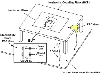
In the test standard of IEC 61000-4-2 [2], two test modes have been specified: air-discharge test mode and contact-discharge test mode. Fig. 1 shows the measurement setup of the system-level ESD test with indirect contact-discharge test mode, which consists of a wooden table on the grounded reference plane (GRP). In addition, an isolation plane is used to isolate the EUT from horizontal coupling plane (HCP). The HCP are connected to the GRP with two 470kΩ resistors in series.
With the measurement setup in Fig. 1, the robustness of CMOS ICs in the EUT against the system-level ESD stress can be determined. The transient responses on power lines of CMOS ICs can be further analyzed and recorded by the oscilloscope. Thus, the circuit performance of the proposed transient detection circuit can be evaluated through this measurement setup.
Fig. 1. Measurement setup for system-level ESD test with indirect contact-discharge test mode.
III. TRANSIENT DETECTION CIRCUIT
A. Circuit Structure
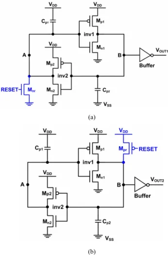
The proposed transient detection circuits realized with NMOS-reset and PMOS-reset functions are shown in Figs. 2(a) and 2(b), respectively. The detection circuits, composed of one latch and two coupling capacitances, are designed to memorize the occurrence of system-level ESD events and to sense the fast electrical transient on the power and ground
IEEE 2006 Custom Intergrated Circuits Conference (CICC)
lines. The detection circuits shown in Figs. 2(a) and 2(b) are realized with 3.3V devices in a standard 0.13-µm CMOS process for 3.3-V circuit applications. The output signal of proposed on-chip transient detection circuit with NMOS-reset function is VOUT1, and the output signal of proposed on-chip
transient detection circuit with PMOS-reset function is VOUT2.
(a)
(b)
Fig. 2. The proposed on-chip transient detection circuits realized with (a) NMOS-reset, and (b) PMOS-reset, functions.
In order to increase the operation speed of detection circuit in Figs. 2(a) and 2(b) during fast electrical transient under the system-level ESD zapping, the device ratios (W/L) of latch should be adjusted. In order to pull down the voltage level of node B easily, the NMOS (Mn1) in the inverter1 (inv1) is
designed with a larger W/L than that of PMOS (Mp1). On the
contrary, to pull up the voltage level of node A easily, the PMOS (Mp2) in the inverter2 (inv2) is designed with a larger
W/L ratio than that of NMOS (Mn2). In order to enhance the
sensitivity of the detection circuit to electrical transient, two capacitances (CP1 and CP2) are added between the node A (B)
and VDD (VSS). The capacitance CP1 is placed between the
VDD and the input of inv1 in order to sense fast electrical
transient on VDD. The capacitance CP2 is placed between the
VSS and the input of inv2 in order to sense fast electrical
transient on VSS. The NMOS (Mnr) in Fig. 2(a) and the PMOS
(Mpr) in Fig. 2(b) are used to provide the reset function in
order to avoid the metastable operation of the latch circuit. With the reset signal of 3.3V (0V), the node A (B) of the
detection circuit shown in Figs. 2(a) (Fig. 2(b)) can be initially set up to 0V (3.3V). In normal condition, the output (VOUT1 and VOUT2) of the proposed transient detection circuits
will be kept at logic “0”. When a system-level ESD event occurs, the fast transient noises injecting to the power lines (VDD, VSS) will change the output state from logic “0” to
become logic “1”. Therefore, the system-level ESD event can be detected by the proposed detection circuits.
The sensitivity of the proposed transient detection circuit can be further analyzed by adjusting the device ratios (W/L) in the latch or changing the value of coupling capacitances.
B. Simulation
A simulation tool (HSPICE) is used to investigate the on-chip detection circuit performance under the system-level ESD test. In this simulation tool, a specific time-dependent voltage source given by
( )= a⋅sin(2π ( − d)) exp( (⋅ − − d) a)
V t V f t t t t D (1)
is used to apply an underdamped sinusoidal voltage on the power lines of the proposed transient detection circuits. In the following HSPICE simulation, with the proper parameters such as the applied voltage amplitude Va, damping factor Da, damping frequency f, and time delay td, the intended underdamped sinusoidal voltage can be constructed.
On the printed circuit board layout, the routing traces may be different for power lines and ground lines. This can cause different coupling paths from ESD stress source to VDD and
VSS pins of the chip, as shown in Fig. 3. The different
coupling paths will result in different coupling delay between VDD and VSS waveforms. Thus, the proposed transient
detection circuit should be evaluated in the conditions, where there is some coupling delay influence on VDD/VSS.
Fig. 3. Different coupling paths on printed circuit board from ESD stress source to VDD and VSS pins of ICs.
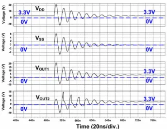
Under the condition of no coupling delay influence on VDD/VSS, the simulated VDD, VSS, VOUT1, and VOUT2
waveforms of the proposed transient detection circuit with a positive-going underdamped sinusoidal voltage on both VDD
and VSS are shown in Fig. 4. The positive-going underdamped
sinusoidal voltage with Va of +20V is used to simulate the positive ESD stress under the system-level ESD test. The VDD
voltage is initially kept at 3.3V with VSS of 0V. Under ESD 362
stress, VDD/VSS begins to increase rapidly from 3.3V/0V.
VOUT1 and VOUT2 are disturbed simultaneously during VDD/VSS
disturbance. During this period, the transient detection circuit can detect the occurrence of disturbance on VDD/VSS. As a
result, after VDD finally returns to its normal voltage level of
3.3V, VOUT1 and VOUT2 will be changed from 0V to 3.3V.
Fig. 4. Simulated VDD, VSS, VOUT1, and VOUT2 waveforms of the proposed
transient detection circuits with positive-going underdamped sinusoidal voltage on both VDD and VSS.
Fig. 5. Simulated VDD, VSS, VOUT1, and VOUT2 waveforms of the proposed
transient detection circuit with negative-going underdamped sinusoidal voltage on both VDD and VSS.
Under the condition of no coupling delay influence on VDD/VSS, the simulated VDD, VSS, VOUT1, and VOUT2
waveforms of the proposed transient detection circuit with a negative-going underdamped sinusoidal voltage on both VDD
and VSS are shown in Fig. 5. The negative-going
underdamped sinusoidal voltage with Va of -20V is used to simulate the negative ESD stress under the system-level ESD test. The VOUT1 and VOUT2 are influenced by the VDD/VSS
disturbance through coupling paths. Finally, the outputs (VOUT1 and VOUT2) of the transient detection circuits are
changed from 0V to 3.3V.
The simulated VDD, VSS, VOUT1,andVOUT2 waveforms of
the proposed transient detection circuit with a coupling delay
of 8ns between VDD and VSS are shown in Fig. 6. During the
period with fast transient stress, VOUT1 and VOUT2 are
influenced by the VDD/VSS disturbance. Finally, VOUT1 and
VOUT2 are pulled up to the voltage level of 3.3V. With a
coupling delay between VDD and VSS, the proposed transient
detection circuit can still memorize the occurrence of fast ESD transient stress.
From these simulations, the output states of detection circuits can be changed and kept at logic “1”, after the system-level ESD events. The sensitivity of the ESD detection circuits on the electrical transient stress can be analyzed by changing the coupling capacitances between the nodes A (B) and VDD (VSS) or by changing the device ratios
(W/L) in the latch. The HSPICE simulation can be used to fine tune the device sizes in the proposed transient detection circuits to detect different transient levels.
Fig. 6. Simulated VDD, VSS, VOUT1, and VOUT2 waveforms of the proposed
transient detection circuit with a coupling delay of 8ns between VDD and VSS.
IV. EXPERIMENTALRESULTS
The proposed on-chip transient detection circuits have been fabricated in a 0.13-µm 1.2/3.3-V 1P8M CMOS process. The system-level ESD test with indirect contact-discharge test mode is used to experimentally verify the proposed transient detection circuit. With both positive and negative fast electrical transient, the measured VDD transient response can
be recorded by the oscilloscope. This can clearly indicate whether the detection circuit works correctly during the system-level test.
The measured VDD and VSS waveforms of the proposed
transient detection circuit with ESD voltage of +500V zapping on the HCP under system-level ESD test are shown in Fig. 7. A coupling delay of ~5ns between VDD and VSS has
been found in Fig. 7. This measured result is consistent with the design consideration shown in Fig. 3 and Fig. 6.
The measured VDD, VOUT1,and VOUT2 waveforms of the
proposed transient detection circuit with ESD voltage of +1500V zapping on the HCP under system-level ESD test are shown in Fig. 8. VDD begins to increase rapidly from the
normal voltage (+3.3V). Meanwhile, VOUT1 and VOUT2 begin 363
to greatly increase with such high-energy ESD stress. During the period with disturbance on VDD, VOUT1 and VOUT2 are
disturbed simultaneously. Finally, the output voltage of the transient detection circuit is changed from 0V to 3.3V. As a result, the transient detection circuit can memorize the occurrence of the system-level ESD stress. The experimental results in Fig. 8 are consistent with the HSPICE simulation results in Fig. 4.
Fig. 7. Measured VDD and VSS transient responses with ESD voltage of
+500V zapping on the HCP under system-level ESD test. There is a coupling delay of ~5ns between VDD and VSS waveforms in the initial period during the
fast transient stress.
Fig. 8. Measured VDD, VOUT1, and VOUT2 transient responses with ESD
voltage of +1500V zapping on the HCP under system-level ESD test. The measured VDD, VOUT1,and VOUT2 transient waveforms
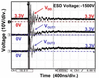
of the proposed transient detection circuits with ESD voltage of -1500V zapping on the HCP under system-level ESD test are shown in Fig. 9. During VDD disturbance, VOUT1 and
VOUT2 are disturbed simultaneously. Obviously, VOUT1 and
VOUT2 are finally pulled up to the 3.3V after the fast electrical
noise.
The circuit performance of the transient detection circuit under the system-level ESD test has been proved by both the experimental results in silicon chip and the HSPICE simulation. From the experimental results, the proposed transient detection circuit can indeed memorize the occurrence of system-level ESD stress.
Fig. 9. Measured VDD, VOUT1, and VOUT2 transient responses with ESD
voltage of -1500V zapping on the HCP under system-level ESD test. V. CONCLUSION
A new transient detection circuit for system-level ESD protection has been implemented in a CMOS 0.13-µm process. By using one latch logic gate and two coupling capacitances, the on-chip transient detection circuit can be designed to detect the fast electrical transient during the system-level ESD zapping. The circuit performance under different positive and negative fast electrical transient has been also investigated by HSPICE. The experimental results in silicon chip have confirmed that the proposed on-chip transient detection circuit can detect fast electrical transients during system-level ESD zapping. The proposed transient detection circuit can be further combined with firmware design and power-on reset circuit to provide an effective solution to solve the system-level ESD issue in microelectronics system with CMOS ICs.
REFERENCES
[1] M.-D. Ker and S.-F. Hsu, “Physical mechanism and device simulation on transient-induced latchup in CMOS ICs under system-level ESD test,” IEEE Trans. Electron Devices, vol. 52, no. 8, pp. 1821–1831, Aug. 2005.
[2] IEC 61000-4-2 Standard, “EMC – Part 4-2: Testing and measurement techniques – Electrostatic discharge immunity test,” IEC, 2001. [3] M.-D. Ker and Y.-Y. Sung, “Hardware/firmware co-design in a 8-bits
microcontroller to solve the system-level ESD issue on keyboard,” in Proc. EOS/ESD Symp., 1999, pp. 352–360.
[4] M.-D. Ker and S.-F. Hsu, “Evaluation on board-level noise filter network to suppress transient-induced latchup under system-level ESD test,” in Proc. EOS/ESD Symp., 2005, pp. 178–189.
[5] M. I. Montrose, Printed Circuit Board Design Techniques for EMC Compliance, IEEE Press, 2000.
[6] H. W. Ott, Noise Reduction Techniques in Electronic Systems, 2nd
Edition, John Wiley & Sons, 1988.
364